
 Open Access Article
 This Open Access Article is licensed under a Creative Commons Attribution-Non Commercial 3.0 Unported Licence
A facile solution processible self-rectifying and sub-1 V operating memristor via oxygen vacancy gradient within a TiO2 single layer†
Min Ho
Park
ab,
Jun Hyung
Jeong
ab,
Wonsik
Kim
c,
Soohyung
Park
cd,
Byeong Min
Lim
ab,
Hong-Sub
Lee
ab and
Seong Jun
Kang
 *ab
*ab
aDepartment of Advanced Materials Engineering for Information and Electronics, Kyung Hee University, Yongin, 17104, Republic of Korea. E-mail: junkang@khu.ac.kr; Tel: +82-31-201-3324
bIntegrated Education Program for Frontier Materials (BK21 Four), Kyung Hee University, Yongin, 17104, Republic of Korea
cAdvanced Analysis Center, Korea Institute of Science and Technology, 5 Hwarang-ro 14-gil, Seongbuk-gu, Seoul 02792, Republic of Korea
dDivision of Nano & Information Technology, KIST School, University of Science and Technology (UST), Seoul 02792, Republic of Korea
First published on 16th April 2024
Abstract
Memristors are becoming increasingly recognized as candidates for neuromorphic devices due to their low power consumption, non-volatile memory, and synaptic properties and the ease of parallel computing through crossbar arrays. However, sneak current is a critical obstacle in crossbar arrays, and much research is being conducted to suppress the sneak current through self-rectifying characteristics. Here, we present a highly straightforward method for fabricating an active layer of a self-rectifying memristor through a single spin coating process, capitalizing on the attributes of spin coating, which initiates the reaction from the upper portion of the solution. We fabricated a self-rectifying memristor using an Ag/TiO2/TiOx/ITO structure through a vacuum-free solution process with low cost. During the spin-coating process, the reaction between titanium isopropoxide (TTIP) and ambient moisture formed TiO2 with an oxygen vacancy gradient. We confirmed the natural oxygen vacancy gradient using X-ray photoelectron spectroscopy (XPS) depth profiling and elucidated the resistance switching and self-rectifying mechanisms of the memristor based on the energy band structure. The memristors exhibited resistance switching and self-rectifying characteristics, which were essential characteristics for preventing sneak currents in a 3 × 3 crossbar array structure.
1. Introduction
Recently, memristors have been extensively studied as the next-generation non-volatile memory devices owing to their low power consumption and synaptic characteristics.1–4 Conventional memristors are composed of a simple two-terminal device consisting of a metal–insulator–metal structure, predominantly using oxide-based insulators such as TiOx, TaOx, AlOx and HfOx.5–9 These metal oxide-based memristors can broadly be categorized into two types: filament type and interface type. In the filament type memristor, the formation of conductive filaments is observed due to ion migration. Furthermore, switching between a low resistance state (LRS) and a high resistance state (HRS) is facilitated by the formation or rupture of a conductive filament, which is a few nanometers wide, in response to an externally applied electric field.10,11 On the other hand, in the case of interface type memristors, switching between the HRS and LRS is driven by the migration of oxygen vacancies and the consequent change in contact resistance such as the Schottky barrier height, leading to gradual resistance changes.12,13 Interface type memristors have an advantage in reliability over filament type memristors due to the absence of the irregular forming process required.14,15 However, they exhibit poorer retention properties than filament type memristors, due to the detrapping of electrons and the diffusion of oxygen vacancies from the interface to the bulk.16,17 These switching characteristics make them useful as memory devices. Memristors are two-terminal devices, as opposed to traditional three-terminal memory devices based on transistors. Therefore, memristors offer advantages in increasing memory integration through a crossbar array architecture. The crossbar array architecture, a parallel circuit structure similar to human neural networks, facilitates parallel computing and offers remarkable efficiency in artificial neural networks (ANNs).18–20 Because of these advantages, memristor crossbar arrays emerge as promising candidates for neuromorphic applications. However, there is a serious obstacle called sneak current through sneak paths in the memristor crossbar arrays. Reading of high resistance state (HRS) cells is obstructed by sneak current flowing through adjacent low resistance state (LRS) cells.10,21 Sneak current can be eliminated by connecting various devices in series, such as a diode,22,23 transistor24,25 and metal–insulator switching devices.26,27 However, this approach has the drawback of inducing a voltage drop, which deteriorates the performance of memristors, and it also introduces added complexity to the device fabrication process. In this respect, self-rectifying memristors offer significant advantages as they can suppress sneak currents induced by reverse bias without requiring additional devices in the crossbar array.8,28It is very challenging for single active-layer memristors to exhibit self-rectifying characteristics because they are predominantly of the filament type. In the case of filament type memristors, conductive filaments are formed and broken due to ion migration in response to bias, resulting in the transition between the LRS and HRS.6–9,29,30 These conductive filaments are inherently incapable of exhibiting self-rectification, which leads to sneak currents in a crossbar array. Furthermore, the formation of these conductive filaments is highly irregular, and controlling the filament size is very difficult.31 Therefore, numerous research efforts aim to inhibit the sneak current path through interface type memristors, capitalizing on features such as complementary resistive switching (CRS) or self-rectifying characteristics. Leung et al. reported a CRS memristor composed of TiOx/TiO2/TiOx active layers to suppress leakage current, but the current–voltage (I–V) characteristics showed a small hysteresis window due to the CRS structure.32 Meanwhile, much research has also focused on self-rectifying characteristics using multi-active layers such as TiO2/HfO2, HfO2/TaOx, Ta2O5/HfOx, and NbOx/TiOy/NbOx structures.33–36 However, these approaches require highly precise atomic layer deposition (ALD) processes, leading to complexity due to additional fabrication steps. Furthermore, a voltage drop occurs owing to energy barriers between the active layers or insulating layers.
In this work, we fabricated a single TiO2 active layer with an oxygen vacancy gradient through a very simple spin coating process, considering that only the top of the solution is exposed to the atmosphere during the spin coating.37,38 The single TiO2 thin film formed a TiO2/TiOx structure due to the oxygen vacancy gradient, and high-resolution transmission electron microscopy (HR-TEM) and X-ray photoelectron spectroscopy (XPS) depth profiling were used to observe the oxygen vacancy gradient within the single TiO2 thin film. In addition, we demonstrated resistive switching, low voltage operating and self-rectifying characteristics in a fabricated Ag/TiO2/TiOx/ITO using the spin coating method. The TiO2 based memristor in 3 × 3 crossbar array could retain the LRS and HRS in individual cells, and the synaptic function of the device was investigated.
2. Experimental
Preparation of TiO2 thin films
We synthesized three different types of TiO2 thin films using distinct TiO2 solutions and spin coating conditions. The TiO2 thin films are abbreviated as follows: a-TiO2 spin-coated under ambient conditions, g-TiO2 spin-coated in a glove box, and s-TiO2 fabricated using a sol–gel solution. 0.33 M titanium isopropoxide (TTIP) solution used to prepare a-TiO2 and g-TiO2 thin films was synthesized by adding 1 ml of TTIP (SAM CHUN) to 10 ml of ethanol. The vial containing the solution was sealed to prevent the hydrolysis reaction caused by moisture, and the TTIP solution was vigorously stirred for 1 h. The as-prepared TTIP solution was spin-coated onto an indium tin oxide (ITO)/glass substrate at 6000 rpm for 30 s. It was then pre-annealed at 150 °C for 10 min, followed by post-annealing at 350 °C for 1 h, resulting in the fabrication of a TiO2/TiOx film with an oxygen vacancy gradient. For a-TiO2, both spin-coating and annealing were conducted under ambient conditions, with the relative humidity ranging from 35 to 45%. In contrast, for g-TiO2, spin coating and pre-annealing were carried out in a glove box under an N2 atmosphere, while post-annealing was carried out under ambient conditions. To fabricate s-TiO2, a sol–gel solution was prepared by stirring 1 ml of 0.33 M TTIP solution and 10 μl of 36 wt% aqueous HCl for 1 h to achieve homogeneous and slow hydrolysis.39 s-TiO2 was fabricated by spin-coating the sol–gel solution, with the same spin-coating and annealing conditions as those for a-TiO2.Device fabrication
An ITO/glass substrate with a sheet resistance of 15 Ω sq−1 (size: 15 mm × 15 mm) was used as the bottom electrode. Dot type memristors used bare ITO, whereas crossbar type memristors used ITO patterned in three bar shapes (size: 15 mm × 1 mm). The ITO electrode was patterned using a positive photoresist (PR) (AZ 5214, AZ Electronic Materials) through conventional photolithography and a wet etching process using HCl as the etchant. The ITO/glass substrate was ultrasonicated sequentially with DI water, acetone and isopropyl alcohol. The cleaned ITO/glass substrate was treated with UV-ozone for 20 min to increase the ITO work function.40 Following this, the TiO2 thin film was deposited on ITO through spin-coating and annealing processes. Next, a photolithography process was performed to define the top electrode size. A positive PR was spin-coated on at 6000 rpm for 30 s, followed by baking at 120 °C for 3 min. The PR layers were patterned by UV light exposure through a metal mask and then developed using 2.38 wt% tetramethylammonium hydroxide in water. The size of the developed patterns was 1000 μm × 1000 μm for the dot type and 1500 μm × 100 μm for the crossbar type. After hard baking at 150 °C for 10 min, an Ag paste (P-100, CANS) top electrode was spread on the pattern using a needle. Finally, the Ag paste was hardened by annealing at 100 °C for 20 s, completing the Ag/TiO2/TiOx/ITO structure memristor. Schematic structures of dot type and crossbar type devices are shown in Fig. S1 (ESI†).Characterization
HR-TEM images and energy-dispersive spectroscopy (EDS) data were obtained using a field emission electron microscope (JEM-2100F, JEOL). XPS and ultraviolet photoelectron spectroscopy (UPS) measurements were conducted using a surface analysis system (NEXSA, Thermo fisher) with an Al Kα (1486.6 eV) source for XPS and a He I (21.22 eV) source for UPS. The energy references of the XPS and UPS spectra were calibrated with respect to the Fermi level of a clean Au sample. For XPS depth profiling, Ar etching was carried out and 4 keV Ar+ ion beam was used as the etching source. The I–V characteristics were measured using a two probe measurement system with a source meter unit (2400, Keithley) under ambient conditions. Synaptic characteristics of the device, including potentiation and depression, were measured using a source meter unit (2634B, Keithley).3. Results and discussion
As a result, hydrolysis proceeds rapidly in the upper portion of the solution exposed to the atmosphere, while in the lower portion of the solution, the hydrolysis reaction occurs much more slowly. After annealing, the upper part of the thin film is converted into stoichiometric TiO2, whereas the lower part of the thin film is converted into TiOx with large amounts of defects. Consequently, the a-TiO2 single layer forms the TiO2/TiOx structure.41–43 We anticipated that the partially formed TiOx would exhibit self-rectifying characteristics in memristors. Fig. 1b shows a cross-sectional HR-TEM image of a crystalline a-TiO2 thin film formed on an ITO substrate, with the inset displaying a fast Fourier transform (FFT) image of the a-TiO2 thin film. The angles indicated in the FFT image are 82° and 49°, which are identical to the theoretical values for the angles between the (101) and (011) crystal planes of anatase.44,45 Due to the process involving a single spin-coating step for thin film formation, the TiO2/TiOx interface boundary could not be identified in HR-TEM images. However, the formation of TiOx and the differences between the upper and lower parts of the thin film were verified. In the HR-TEM image of a-TiO2, the atomic plane spacing was 3.50 nm for 10 atomic planes (d-spacing: 0.350 nm) in the upper portion of a-TiO2, while in the lower portion of a-TiO2, it was 3.54 nm for 10 atomic planes (d-spacing: 0.354 nm). The d-spacing value in the upper part of a-TiO2 was consistent with the reported d-spacing value of anatase.44–46 However, the d-spacing of the lower part of a-TiO2 is slightly larger, indicating the presence of defects, such as Ti3+ ions, oxygen vacancies and hydroxyl groups, in the lower part of a-TiO2. Fig. 1c presents the overall elemental distribution of C, O, Ti, Si and In atoms and quantitatively compares the element counts based on EDS line scan results. Ti counts were higher in the lower part of a-TiO2 than in the upper part, while O counts remained relatively uniform. This indicates the presence of the TiOx phase in the lower part of the a-TiO2 thin film. The HR-TEM image (scale bar: 100 nm) and EDS mapping images in Fig. S2 (ESI†) indicate that the a-TiO2 thin film was formed uniformly.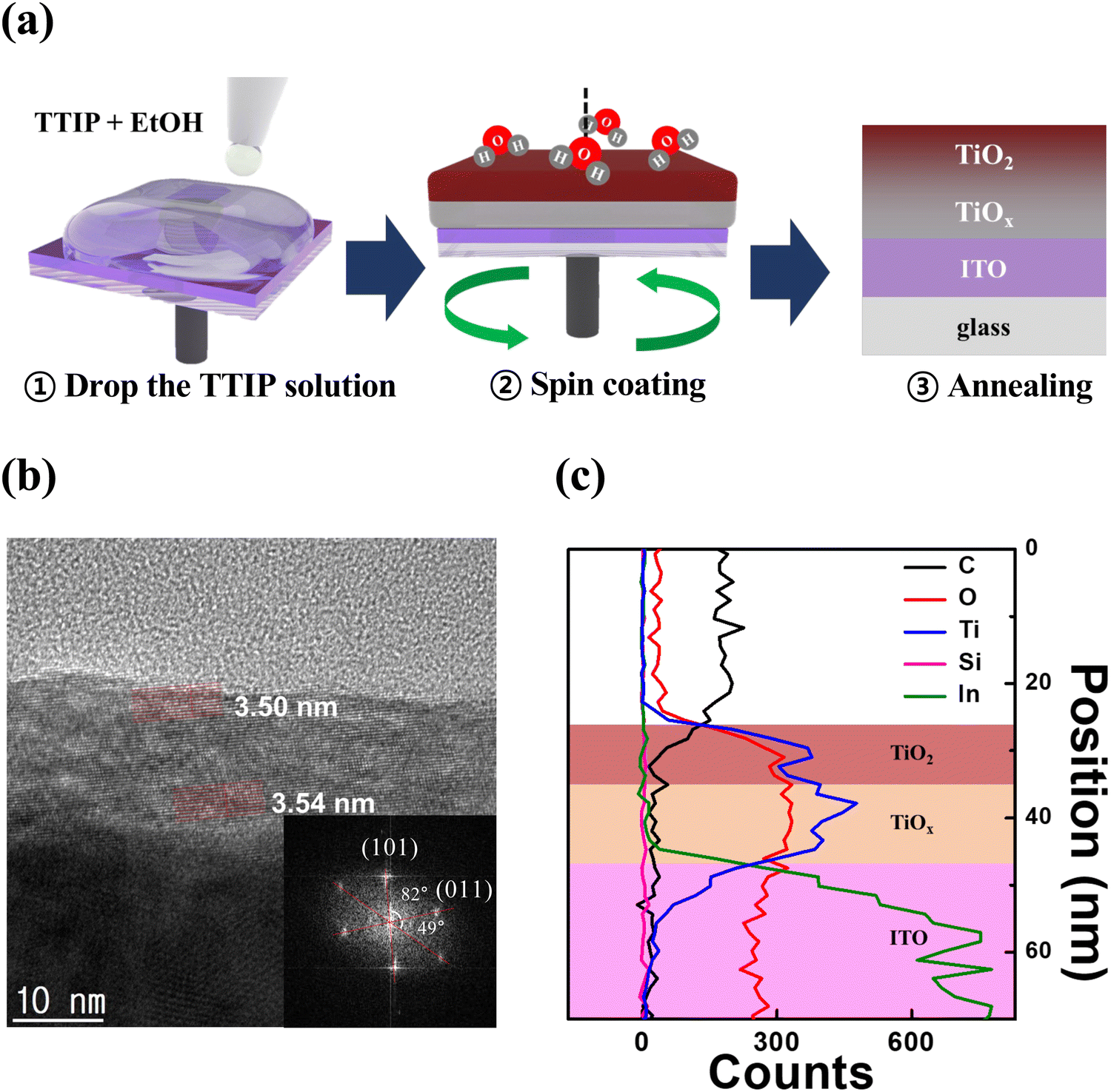 | ||
| Fig. 1 Formation of a TiO2/TiOx structure. (a) Schematic diagram of spin coating of an a-TiO2 thin film using the TTIP solution. (b) Cross-sectional HR-TEM image of a crystalline a-TiO2 thin film on an ITO substrate and FFT image (inset). (c) EDS elemental line of the a-TiO2 thin film on the ITO substrate. | ||
To investigate the difference in chemical bonding between the upper and lower portions of the a-TiO2 thin films, XPS depth analysis was conducted. Fig. 2 depicts the XPS spectra of the Ti 2p and O 1s regions of the a-TiO2 thin film on an ITO substrate, respectively, as functions of sputtering time. As shown in Fig. 2a, two prominent peaks were observed in the Ti 2p region of the XPS spectra at approximately 459.3 eV and 465.1 eV before etching a-TiO2. The separation between these peaks is representative of Ti 2p3/2 to Ti 2p1/2 spin–orbital splitting, originating from Ti4+ in TiO2.47,48 It is observed that these two spectra have different full width at half maximum (FWHM) values due to the Coster–Kronig effect.49 The XPS spectra of the upper portion of a-TiO2 exclude Ti3+ and Ti2+ peaks at around 457.5 eV and 455.5 eV.50 However, after etching the a-TiO2 thin film, shoulder peaks appeared at around 458 and 455 eV, indicating the presence of Ti3+ and Ti2+. Moreover, the shoulder peaks also intensified as the etching time increased, and etching for over 50 s revealed the presence of In 3d peaks originating from the underlying ITO substrate.51 Additionally, after etching for more than 50 s, the low binding energy shift of the Ti4+ peak was caused by adjacent indium and tin atoms.52,53 Therefore, the XPS depth analysis of Ti 2p reveals that the upper portion of a-TiO2 exists in the TiO2 phase, and the content of TiOx increases further down in the lower part of a-TiO2. The lattice oxygen (OL) peak at around ∼530.5 eV shifts to a higher binding energy with an increase in etching time, and the shoulder peak between 531 and 533 eV appears due to the presence of oxygen vacancies (Vo) and hydroxyl groups, as shown in Fig. 2b.54 After etching for more than 50 s, the OL peak shifted to a lower binding energy influenced by the ITO substrate. Many studies have reported that TiOx containing Ti3+ ions induces the formation of Vo.32,55,56 Therefore, the XPS O 1s depth profiles show the same tendency as the XPS Ti 2p depth profiles, indicating the presence of the oxygen vacancy gradient within the a-TiO2 thin film.
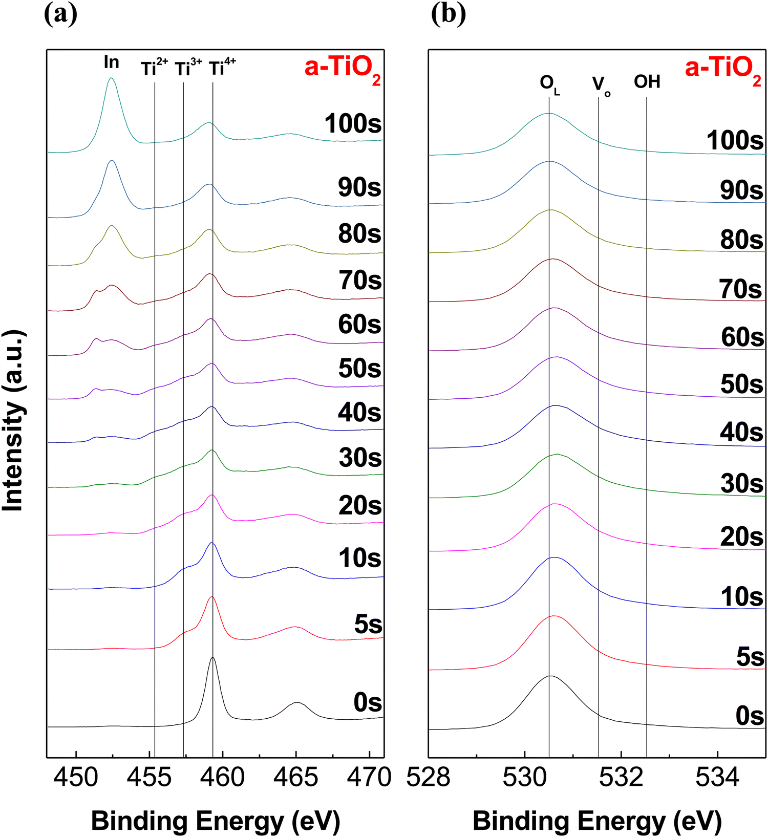 | ||
| Fig. 2 XPS depth profile for (a) Ti 2p and (b) O 1s in the as-prepared a-TiO2 film on the ITO substrate. | ||
We compared a-TiO2 spin-coated under ambient conditions, g-TiO2 spin-coated in a glove box under an N2 atmosphere, and s-TiO2 fabricated using a sol–gel solution to retard the hydrolysis reaction with moisture. This comparison was aimed at demonstrating that the oxygen vacancy gradient in a-TiO2 originates from the reaction with atmospheric moisture during spin-coating. As shown in Fig. S3 (ESI†), XPS depth analysis was also carried out on the g-TiO2 and s-TiO2 thin films. Fig. 3 shows the Ti 2p and O 1s XPS spectra of various TiO2 thin films at etching times of 0 s, 10 s and 30 s, respectively. As shown in Fig. 3a, the upper portion of several TiO2 thin films exhibits peaks at ∼459.3 and ∼465.1 eV, with no observable peak indicative of Ti3+ and Ti2+. This indicates that the surfaces of a-TiO2, g-TiO2, and s-TiO2 are all in nearly defect-free TiO2 states. However, in the Ti 2p XPS spectra at an etching time of 10 s (Fig. 3b), a decrease in the Ti4+ peak and the appearance of a shoulder peak corresponding to Ti3+ are observed, regardless of the type of TiO2. In addition, in the Ti 2p XPS spectra at an etching time of 30 s (Fig. 3c), the Ti4+ peak decreased more significantly compared to that at an etching time of 10 s, while the Ti2+ and Ti3+ peaks increased prominently. Notably, in the case of a-TiO2, the increase in Ti3+ and Ti2+ peaks was not as prominent, and the presence of Ti2+ was relatively limited. The Ti 2p XPS depth profile results indicate the existence of a gradual TiOx state as a function of the depth within a-TiO2, which exhibits a more natural oxygen vacancy gradient of the TiOx state compared to g-TiO2 and s-TiO2. Moreover, it suggests that the chemical bonding composition in the lower portion of a-TiO2 is distinct from that of the lower portions in g-TiO2 or s-TiO2. To analyze the different types of TiO2 chemical bonds, the O 1s spectra were deconvoluted into three peaks using the Gaussian–Lorentzian fitting. The peaks centered at binding energies of ∼530.5, ∼531.5 and ∼532.6 eV indicate the presence of OL, Vo and hydroxyl groups, respectively. As shown in Fig. 3d–f, the XPS O 1s spectra of unetched TiO2 films exhibited similar surface characteristics, consistent with the observed trends in the Ti 2p spectra, regardless of the spin-coating conditions used for TiO2 film deposition. However, the O 1s spectra of TiO2 films etched for 30 s exhibited differences attributable to the spin-coating conditions, as shown in Fig. 3g–i. The lower portion of a-TiO2 exhibited a significantly higher concentration of Vo compared to its surface, and this concentration was also notably higher than that observed in the lower portions of g-TiO2 and s-TiO2. Additionally, as shown in Fig. S4 (ESI†), a-TiO2 exhibited a higher Vo concentration compared to g-TiO2 and s-TiO2 for all etching time conditions. However, the concentration of hydroxyl groups was significantly lower in etched a-TiO2 compared to etched g-TiO2 and s-TiO2. Fig. S5 (ESI†) summarizes the area ratios of deconvoluted XPS O 1s peaks of TiO2 films for a precise analysis of the depth-dependent characteristics. The depth-dependent oxygen vacancy gradient in TiO2 forms the TiO2/TiOx structure, contributing to self-rectification in memristors. Moreover, natural oxygen vacancy gradient and a larger amount of Vo in a-TiO2 prompt migration of oxygen ions, ultimately enabling low-voltage operation and a high on/off ratio in the memristor.
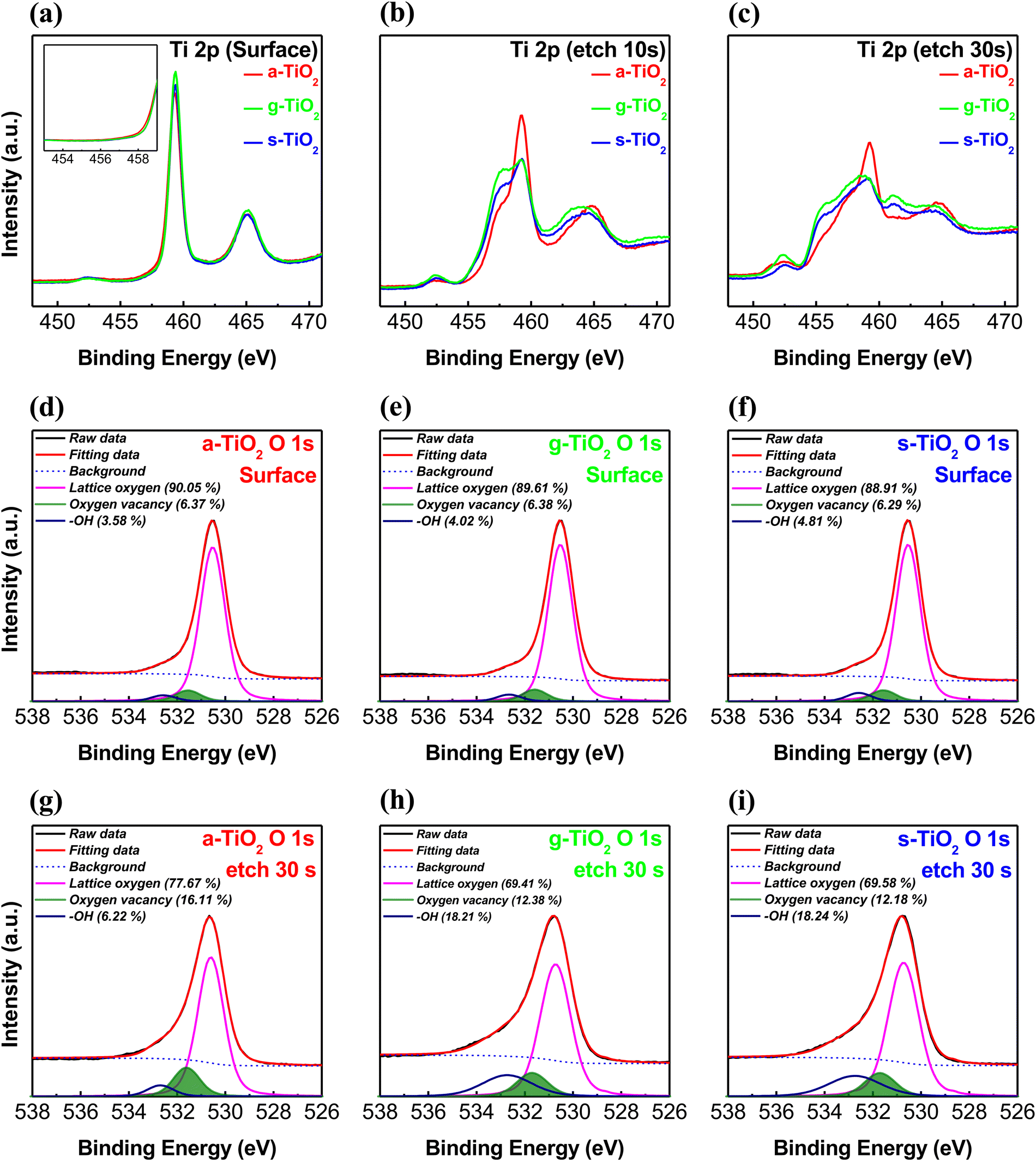 | ||
| Fig. 3 XPS spectra of Ti 2p for a-TiO2, g-TiO2 and s-TiO2 films: (a) under unetched conditions, (b) at an etching time of 10 s, and (c) at an etching time of 30 s. The spectra of O 1s of (d) and (g) a-TiO2, (e) and (h) g-TiO2 and (f) and (i) s-TiO2 films under different etching conditions. | ||
Fig. 4a–c depict the I–V curves of dot type memristors, swept from −0.9 V to 0.9 V over 10 cycles. In Fig. 4a, the red arrows and numbers represent the voltage sweep sequence (under 0 V → 0.9 V → −0.9 V → 0 V), and the I–V curves in Fig. 4b and c were also obtained under the same sweep sequence and bias. All types of memristors exhibited reversible resistance switching and self-rectifying characteristics without the forming process. However, a-TiO2 memristors exhibited superior electrical characteristics compared to g-TiO2 and s-TiO2 memristors. As shown in Fig. 4a, the a-TiO2 memristor initially was at the HRS and rapidly reduced its resistance when the applied bias exceeded 0.25 V, ultimately reaching a compliance current of 1 mA before reaching a bias of 0.9 V. Subsequently, the a-TiO2 memristor exhibited a decrease in current as the bias was reduced to around 0.5 V from the LRS. In contrast, g-TiO2 and s-TiO2 memristors exhibited resistance changes at relatively higher voltages and failed to reach 1 mA even at 0.9 V, as shown in Fig. 4b and c. To precisely confirm the migration of oxygen vacancies and resistance switching at low voltages, 5 cycles at a positive bias of 0.5 V were conducted. As shown in Fig. S6 (ESI†), resistance changes and hysteresis were observed in a-TiO2, whereas no resistance change was noted in s-TiO2 and g-TiO2. This indicates that oxygen vacancy migration occurs under low voltage bias only in a-TiO2, suggesting that the natural gradient of oxygen vacancy concentration significantly facilitates oxygen vacancy migration. The on/off ratio (the ratio of current of LRS to current of HRS at the same voltage) is plotted as a function of bias in Fig. 4d. The maximum on/off ratio of the a-TiO2 memristor exceeded 2 × 10³ at nearly 0.25 V, and the value remained nearly unchanged even after 10 cycle sweeps. In contrast, g-TiO2 and s-TiO2 memristors showed their maximum on/off ratios at relatively higher voltages in the first cycle and significant shifts in the voltage corresponding to the maximum on/off ratio after 10 sweep cycles. Fig. 4e shows the rectification ratio (ratio of the LRS forward current to the LRS reverse current at a certain applied voltage) of the memristors with respect to the sweep cycle number. The maximum rectification ratio of the a-TiO2 memristor was more than 104 in both the first and tenth cycles. However, the maximum rectification ratio of g-TiO2 and s-TiO2 memristors was less than 104 in the first cycle. In the case of g-TiO2, the maximum rectification ratio increased after 10 sweep cycles compared to the first sweep cycle. However, such electrical property changes with cycling are a significant drawback in the devices. As a result, the a-TiO2 memristor, with a larger amount of Vo and the most natural oxygen vacancy gradient, exhibited the best electrical characteristics. Furthermore, the a-TiO2 device exhibited relatively stable electrical properties under voltage sweeps, due to the scarcity of hydroxyl groups, which have the potential to induce device degradation. Additionally, to demonstrate thickness dependency on the switching behavior, we fabricated a-TiO2 memristors using a-TiO2 solutions of various concentrations (0.11 M, 0.33 M, 0.66 M, and 1.32 M). As shown in Fig. S7 (ESI†), in the case of thin films (at 0.11 M), sufficient moisture and TTIP react during spin-coating, resulting in suppressed TiOx formation and, consequently, fewer oxygen vacancies. As a result, the 0.11 M a-TiO2 thin film exhibited insufficient switching behavior, but self-rectifying characteristics were observed. On the other hand, for thicker films (at 0.66 M and 1.32 M), an insufficient reaction occurs between moisture and TTIP, resulting in increased TiOx formation and a higher incidence of oxygen vacancies. Therefore, thicker a-TiO2 films exhibited not only sufficient switching behavior but also self-rectifying characteristics. However, forming processes were observed in thicker films due to excessive oxygen vacancies and need to be avoided in interface memristors. Consequently, these results indicate that achieving stable resistive switching and self-rectifying characteristics in memristors requires thin films of TiO2/TiOx with an appropriate thickness. To compare the performance of our memristor with that of previously reported devices, we summarized our work and previous studies. As shown in Table S1 (ESI†), the a-TiO2 based memristor exhibits remarkable rectification characteristics and low voltage operation.57–66
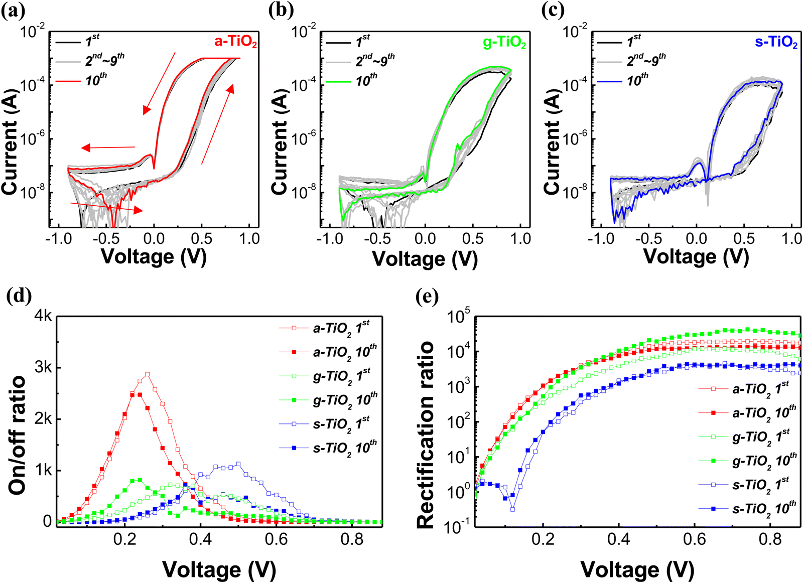 | ||
| Fig. 4 (a)–(c) I–V characteristics of the a-TiO2, g-TiO2 and s-TiO2 memristors, respectively. (d) On/off ratio of a-TiO2, g-TiO2 and s-TiO2 memristors. (e) Rectification ratio of a-TiO2, g-TiO2 and s-TiO2 memristors. | ||
As shown in Fig. S8 (ESI†), UPS measurements were conducted for ITO, a-TiO2, g-TiO2 and s-TiO2 films to elucidate the memristor mechanism based on the energy band structure. Fig. S9 (ESI†) presents the energy band diagram with aligned Fermi level (EF) from the UPS data. Given that the band gap of anatase TiO2 is known to be 3.2 eV,67,68 the energy gap between the conduction band maximum (CBM) state of a-TiO2 and EF was determined to be 1.48 eV. Fig. 5 depicts a simplified schematic diagram of the proposed resistive switching and self-rectifying mechanism for the a-TiO2 based Ag/TiO2/TiOx/ITO memristor. Furthermore, to investigate the conduction mechanism of the Ag/TiO2/TiOx/ITO structure a-TiO2 memristor, the I–V curves were replotted using a log(I)–log(V) plot for the HRS and LRS. As shown in Fig. S10a (ESI†), in the HRS, (1) thermionic Schottky emission, (2) trap-filled limited (TFL) current (slope > 2) and (3) trap-filled limited current (slope ≫ 2) owing to increased trap states from oxygen vacancy migration were sequentially observed as the positive voltage increased.69–71 Due to the natural oxygen vacancy gradient and the highest concentration of Vo, the a-TiO2 memristor achieved TFL conduction at lower voltages than those of s-TiO2 and g-TiO2. In contrast, only trap-free space-charge limited conduction (SCLC) (slope = 2) was observed in the LRS as shown in Fig. S10b (ESI†).72–74 In addition, Ohmic emission attributed to conductive filaments was not observed, which supports the characterization of the Ag/TiO2/TiOx/ITO structure memristor as an interface type. Moreover, as depicted in Fig. S11 (ESI†), utilizing conductive polymer as the top electrode in the PEDOT:PSS/TiO2/TiOx/ITO structure revealed similar I–V characteristics to those of the a-TiO2 memristor. This observation supports that the switching mechanism in our memristor is not driven by conduction filaments associated with metal electrodes. Fig. 5a shows the I–V curve of the a-TiO2 memristor corresponding to the driving mechanism depicted in Fig. 5b–f. The color gradient in the schematic diagrams of the mechanism in Fig. 5b–f represents the degree of Vo, with brighter colors indicating higher concentrations of Vo. As shown in Fig. 5b, the energy barrier inhibits the flow of electrons from ITO to the CBM of a-TiO2 at pristine HRS. Even when considering Vo states, which exist approximately 0.7–1.18 eV below the CBM of TiO2,75,76 it is difficult for current to flow within the device in pristine HRS owing to the relatively low concentration of Vo at the lower portion of a-TiO2. However, as shown in Fig. 5c, Vo accumulate in the lower part of a-TiO2 due to oxygen ion migration during positive voltage application in the top electrode, and electrons begin to flow from ITO to the CBM of a-TiO2 through oxygen vacancy states. The increase in the oxygen vacancy concentration in the lower portion of a-TiO2 induces energy level splitting of Vo, promoting their existence in a broader energy level. As depicted in Fig. 5d, the splitting of Vo levels results in a more favorable flow of electron from ITO to a-TiO2, resulting in the memristor switching to the LRS. Fig. 5e shows the reset process of the memristor during the application of a negative bias to the top electrode. The upper portion of a-TiO2 does not contain Ti3+ and Ti2+ ions, which results in the suppression of Vo migration to the upper portion of a-TiO2 under low negative bias conditions (V > −1 V). As negative bias is applied, oxygen ions migrate towards the lower portion of a-TiO2 and Vo migrate towards the center of a-TiO2. Owing to the absence of Vo in the upper portion of TiO2, a significant energy barrier exists between the TiO2 CBM and Ag, resulting in self-rectifying characteristics.57 Reverse current through the TiO2 CBM is suppressed, but a small amount of current can flow due to electrons trapped in the Vo energy states. As shown in Fig. 5f, applying a reverse bias causes Vo to return to their initial positions, switching the memristor to the HRS.
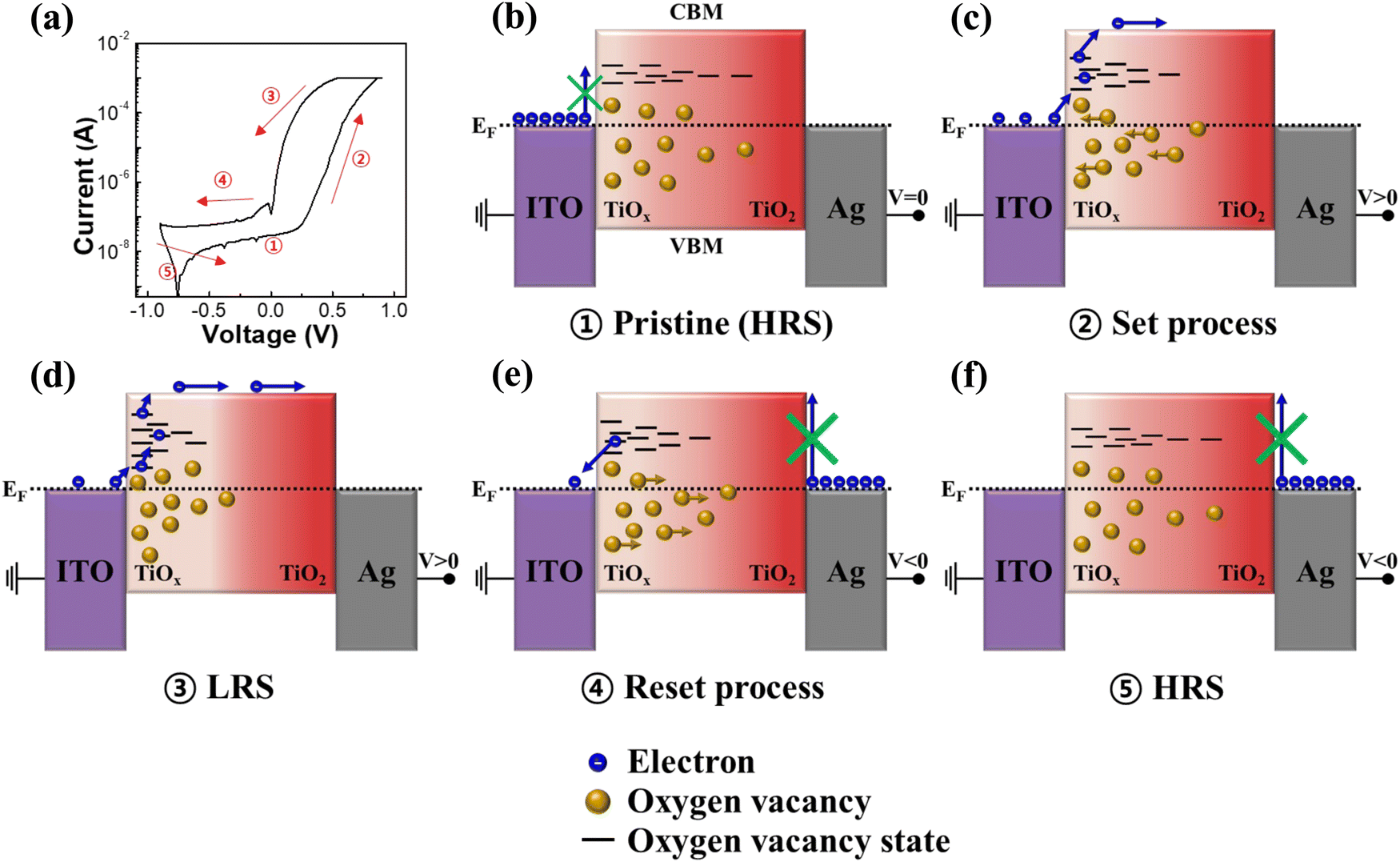 | ||
| Fig. 5 Simplified schematic diagram of the proposed resistive switching and self-rectifying mechanism for the a-TiO2 based Ag/TiO2/TiOx/ITO device. (a) I–V curve of the device. (b) HRS state of the pristine device at V = 0. (c) Set process at V > 0. (d) LRS state at V > 0. (e) Reset process at V < 0. (f) HRS state at V < 0. | ||
To investigate the suppression of sneak current due to self-rectification characteristics, we fabricated a crossbar type device, which was composed of a-TiO2 thin films exhibiting the highest on/off ratio and good stability. Fig. 6a shows the sneak current path in the crossbar array memristor. In conventional crossbar array memristors, the sneak current can flow through adjacent LRS cells during the reading of information from the HRS cell. However, the a-TiO2 memristor with self-rectifying characteristics can effectively suppress all sneak current paths because no current flows in the reverse bias. Fig. 6b shows the I–V curves of all a-TiO2 based 3 × 3 crossbar array type memristors. The self-rectifying characteristics of all 9 devices in the crossbar array were confirmed, demonstrating high uniformity from device to device. Fig. 6c shows the cumulative probability of HRS and LRS conductance for all crossbar array devices in 10 cycles at 0.3 V read voltage, and straight shape plots show superior cycle-to-cycle reliability. The coefficient of variation (Cv) was calculated as the standard deviation divided by the mean value, and Cv values for HRS and LRS conductance were satisfactory at 32.4% and 17.3%, respectively, indicating good reliability. Fig. S12 (ESI†) shows full I–V sweep curves measured during 10 cycles of the 3 × 3 crossbar array memristor. Fig. S13 (ESI†) shows the I–V curves of an a-TiO2 based dot type memristor and a 3 × 3 crossbar array type memristor. The similarity in the I–V characteristics between the dot type and crossbar type memristor provides evidence of effective sneak current suppression in the crossbar array, owing to the self-rectifying characteristics of a-TiO2 based memristors. In particular, it can be observed that the rectification ratio of both crossbar type and dot type devices remained nearly identical across all voltage levels, as shown in Fig. S13b (ESI†). Specifically, in the crossbar type memristor with electrodes 10 times smaller than those of the dot type memristor, the overall current was reduced by nearly tenfold. Specifically, the overall current through the crossbar type devices was reduced by nearly tenfold compared to that of the dot type memristor because the top electrode size of the crossbar type is 10 times smaller than that of the dot type. This is a typical characteristic of interface type memristors that the current is proportional to the active area.13,35,36 Furthermore, this suggests that a-TiO2 memristors can improve power consumption through scaling down. Fig. 6d demonstrates the memorization capability of an a-TiO2 based crossbar array memristor through a “K” shaped information storage. All of the 3 × 3 crossbar array devices were in their HRS before the retention test. A positive bias sweep was conducted on selected devices to store a “K” shaped image in terms of conductance, and the conductance of devices was measured at 0.3 V read voltage, subsequently. Initially, the average LRS/HRS conductance ratio (average conductance of cells with stored “K” shape divided by the average conductance of the remaining cells) was approximately 2.7 times. After 1000 s, the average LRS/HRS conductance ratio was also 2.2 times, and the crossbar array memristor consistently retained the “K” shape as time passed. The retention data for Fig. 6d were plotted with an error bar, as shown in Fig. S14 (ESI†). Owing to rapid electron detrapping and oxygen vacancy diffusion in the absence of an applied voltage, the on/off ratio showed a significant discrepancy. Thus, further study is needed to improve retention issues within single layer base to interface type memristors.16,17Fig. 6e–g show the measured synaptic characteristics such as long-term potentiation (LTP) and long-term depression (LTD) properties using three different write voltages. Both stimulation of potentiation and depression were carried out with 32 pulses and 1 s pulse width. The current exhibits a linear increase when repeating the potentiation pulse (0.4–0.7 V) and a gradual decrease when repeating the depression pulse −0.1 V at 0.1 V read voltage. When the potentiation voltage was 0.4 V, the conductance increase was minimal, while for potentiation voltages of 0.5 V and 0.7 V, the conductance increase exhibited similar trends. However, in all cases, a higher potentiation voltage resulted in a slower occurrence of LTP characteristics. The changes in conductance during potentiation and depression are nearly identical as shown in Fig. 6(e), whereas in Fig. 6(f)–(g), we observe a reduction in depression changes due to the strong potentiation. This result demonstrates the memristor's capability to mimic the LTP and LTD of synaptic weight.
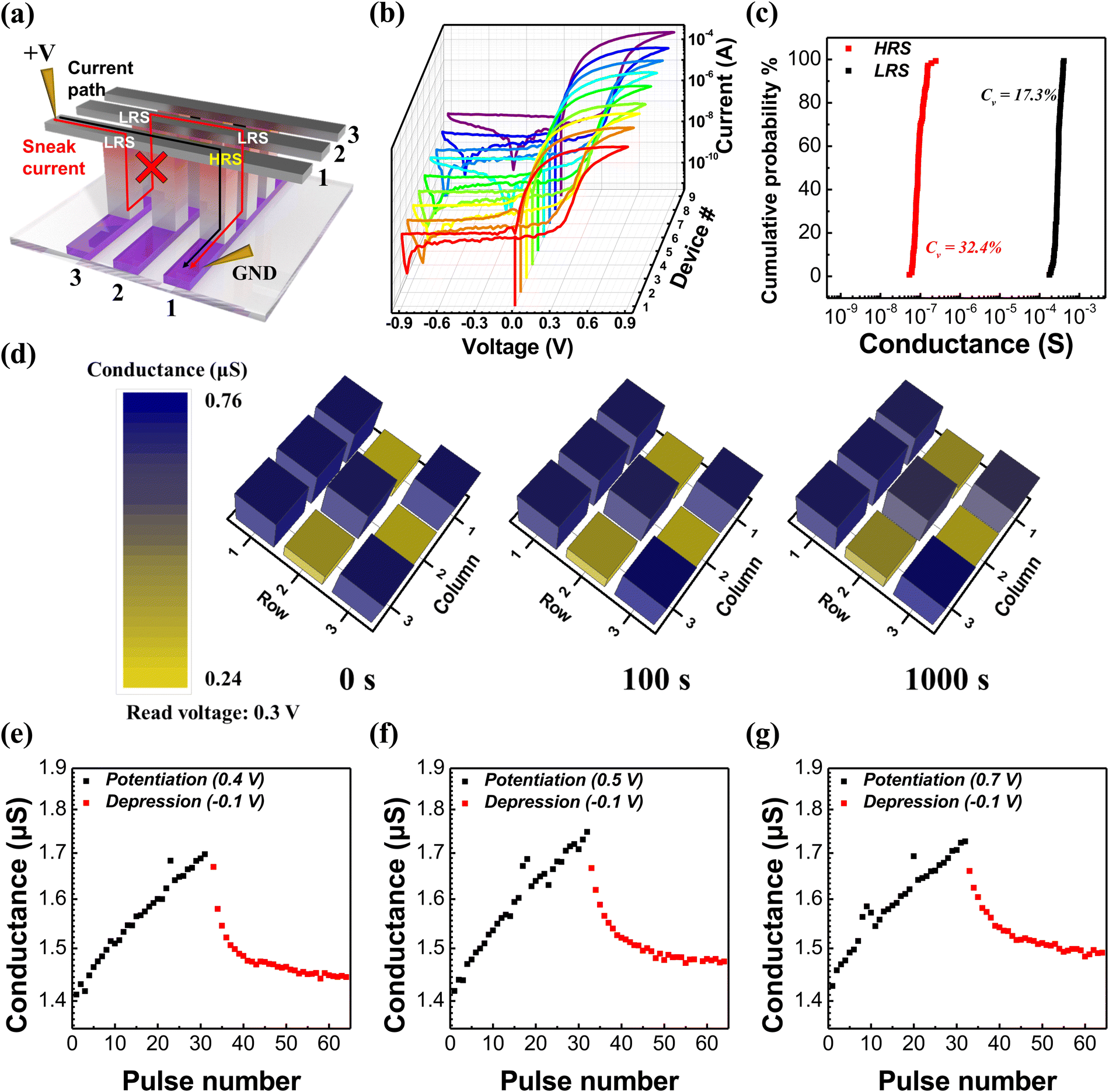 | ||
| Fig. 6 Electrical characteristics of an a-TiO2 based memristor in the 3 × 3 crossbar array. (a) Schematic diagram of the sneak current path in the crossbar array. (b) I–V curves of 3 × 3 crossbar type devices. (c) Cumulative probability of HRS and LRS conductance of 9 devices in 10 cycles (at 0.3 V read voltage). (d) Photograph of the memristor conductance. (e)–(g) LTP and LTD properties of the series memristor measured under different potentiation conditions. | ||
4. Conclusions
We fabricated a memristor with low voltage operation and self-rectifying characteristics, without forming processes in the Ag/TiO2/TiOx/ITO device using a fully vacuum-free solution process. During spin coating, the reaction initially occurs at the top of the solution, leading to the formation of the TiO2/TiOx film. Furthermore, as we approach the bottom of the TiO2 film, a higher concentration of Vo is observed, confirming the presence of a natural oxygen vacancy gradient. The memristors exhibited self-rectifying characteristics due to the TiO2/TiOx structure, and the natural oxygen vacancy gradient led to more significant resistance changes at a low voltage. The device showed a high on/off ratio value of 2 × 10³ and high rectification values of 104 at biases below 0.9 V. The memristor successfully suppressed sneak currents and retained resistance states in a 3 × 3 crossbar array. Thus, our results propose a straightforward method for developing self-rectifying characteristics and low-voltage operation in memristors.Author contributions
Min Ho Park: conceptualization, formal analysis, methodology, investigation, and writing – original draft. Jun Hyung Jeong: formal analysis, methodology, and writing – review & editing. Wonsik Kim: data curation and formal analysis. Soohyung Park: methodology and formal analysis. Byeong Min Lim: data curation and formal analysis. Hong-Sub Lee: methodology and writing – review & editing. Seong Jun Kang: conceptualization, funding acquisition, supervision, and writing – review & editing.Conflicts of interest
There are no conflicts to declare.Acknowledgements
This study was supported by a research project grant from the National Research Foundation of Korea (NRF-2021R1A2C1009442 and 2020R1A6A1A03048004).References
- D. S. Jeong, K. M. Kim, S. Kim, B. J. Choi and C. S. Hwang, Adv. Electron. Mater., 2016, 2, 1600090 CrossRef.
- C. Ma, Z. Luo, W. Huang, L. Zhao, Q. Chen, Y. Lin, X. Liu, Z. Chen, C. Liu and H. Sun, Nat. Commun., 2020, 11, 1439 CrossRef CAS PubMed.
- Y. Wang, Z. Zhang, M. Xu, Y. Yang, M. Ma, H. Li, J. Pei and L. Shi, ACS Appl. Mater. Interfaces, 2019, 11, 24230–24240 CrossRef CAS PubMed.
- C. Zhang, W. B. Ye, K. Zhou, H. Y. Chen, J. Q. Yang, G. Ding, X. Chen, Y. Zhou, L. Zhou and F. Li, Adv. Funct. Mater., 2019, 29, 1808783 CrossRef.
- L. Qingjiang, A. Khiat, I. Salaoru, C. Papavassiliou, X. Hui and T. Prodromakis, Sci. Rep., 2014, 4, 4522 CrossRef PubMed.
- T. Tsuruoka, T. Hasegawa, K. Terabe and M. Aono, Nanotechnology, 2012, 23, 435705 CrossRef PubMed.
- J. Molina, R. Valderrama, C. Zuniga, P. Rosales, W. Calleja, A. Torres, J. D. Hidalga and E. Gutierrez, Microelectron. Reliab., 2014, 54, 2747–2753 CrossRef CAS.
- M. C. Sahu, A. K. Jena, S. K. Mallik, S. Roy, S. Sahoo, R. Ajimsha, P. Misra and S. Sahoo, ACS Appl. Mater. Interfaces, 2023, 25713–25725 CrossRef CAS PubMed.
- K. S. Woo, J. Kim, J. Han, W. Kim, Y. H. Jang and C. S. Hwang, Nat. Commun., 2022, 13, 5762 CrossRef CAS PubMed.
- F. Chen, Y. Zhou, Y. Zhu, R. Zhu, P. Guan, J. Fan, L. Zhou, N. Valanoor, F. Von Wegner and E. Saribatir, J. Mater. Chem. C, 2021, 9, 8372–8394 RSC.
- E. Carlos, J. Deuermeier, R. Branquinho, C. Gaspar, R. Martins, A. Kiazadeh and E. Fortunato, J. Mater. Chem. C, 2021, 9, 3911–3918 RSC.
- Z. Wang, L. Wang, M. Nagai, L. Xie, M. Yi and W. Huang, Adv. Electron. Mater., 2017, 3, 1600510 CrossRef.
- J.-M. Yang, Y.-K. Jung, J.-H. Lee, Y. C. Kim, S.-Y. Kim, S. Seo, D.-A. Park, J.-H. Kim, S.-Y. Jeong and I.-T. Han, Nanoscale Horiz., 2021, 6, 987–997 RSC.
- M. Kim, M. A. Rehman, D. Lee, Y. Wang, D.-H. Lim, M. F. Khan, H. Choi, Q. Y. Shao, J. Suh and H.-S. Lee, ACS Appl. Mater. Interfaces, 2022, 14, 44561–44571 CrossRef CAS PubMed.
- S. Kim, J. Chen, Y.-C. Chen, M.-H. Kim, H. Kim, M.-W. Kwon, S. Hwang, M. Ismail, Y. Li and X.-S. Miao, Nanoscale, 2019, 11, 237–245 RSC.
- W. Zhang, B. Gao, J. Tang, X. Li, W. Wu, H. Qian and H. Wu, Phys. Status Solidi RRL, 2019, 13, 1900204 CrossRef CAS.
- J. Fu, M. Hua, S. Ding, X. Chen, R. Wu, S. Liu, J. Han, C. Wang, H. Du and Y. Yang, Sci. Rep., 2016, 6, 35630 CrossRef CAS PubMed.
- C. Wang, S.-J. Liang, C.-Y. Wang, Z.-Z. Yang, Y. Ge, C. Pan, X. Shen, W. Wei, Y. Zhao and Z. Zhang, Nat. Nanotechnol., 2021, 16, 1079–1085 CrossRef CAS PubMed.
- S. Chen, M. R. Mahmoodi, Y. Shi, C. Mahata, B. Yuan, X. Liang, C. Wen, F. Hui, D. Akinwande and D. B. Strukov, Nat. Electron., 2020, 3, 638–645 CrossRef CAS.
- E. J. Fuller, S. T. Keene, A. Melianas, Z. Wang, S. Agarwal, Y. Li, Y. Tuchman, C. D. James, M. J. Marinella and J. J. Yang, Science, 2019, 364, 570–574 CrossRef CAS PubMed.
- M. A. Zidan, H. A. H. Fahmy, M. M. Hussain and K. N. Salama, Microelectron. J., 2013, 44, 176–183 CrossRef.
- A. Pisarev, A. Busygin, S. Y. Udovichenko and O. Maevsky, Microelectron. J., 2020, 102, 104827 CrossRef.
- J.-J. Huang, Y.-M. Tseng, W.-C. Luo, C.-W. Hsu and T.-H. Hou, 2011 International Electron Devices Meeting, 2011, IEDM11-733 DOI:10.1109/IEDM.2011.6131653.
- C. Li, M. Hu, Y. Li, H. Jiang, N. Ge, E. Montgomery, J. Zhang, W. Song, N. Dávila and C. E. Graves, Nat. Electron., 2018, 1, 52–59 CrossRef.
- X. Feng, S. Li, S. L. Wong, S. Tong, L. Chen, P. Zhang, L. Wang, X. Fong, D. Chi and K.-W. Ang, ACS Nano, 2021, 15, 1764–1774 CrossRef CAS PubMed.
- W. Lee, J. Park, S. Kim, J. Woo, J. Shin, G. Choi, S. Park, D. Lee, E. Cha and B. H. Lee, ACS Nano, 2012, 6, 8166–8172 CrossRef CAS PubMed.
- X. A. Tran, B. Gao, J. F. Kang, X. Wu, L. Wu, Z. Fang, Z. R. Wang, K. L. Pey, Y. C. Yeo, A. Y. Du, M. Liu, B. Y. Nguyen, M. F. Li and H. Y. Yu, 2011 International Electron Devices Meeting, 2011, IEDM11-713 DOI:10.1109/IEDM.2011.6131648.
- T. D. Dongale, G. U. Kamble, D. Y. Kang, S. S. Kundale, H.-M. An and T. G. Kim, Phys. Status Solidi RRL, 2021, 15, 2100199 CrossRef CAS.
- D. Ju, J. H. Kim and S. Kim, J. Alloys Compd., 2023, 170920 CrossRef CAS.
- Y. Abbas, Y.-R. Jeon, A. S. Sokolov, S. Kim, B. Ku and C. Choi, Sci. Rep., 2018, 8, 1228 CrossRef PubMed.
- J. Fu, M. Hua, S. Ding, X. Chen, R. Wu, S. Liu, J. Han, C. Wang, H. Du and Y. Yang, Sci. Rep., 2016, 6, 35630 CrossRef CAS PubMed.
- S. Srivastava, J. P. Thomas, X. Guan and K. T. Leung, ACS Appl. Mater. Interfaces, 2021, 13, 43022–43029 CrossRef CAS PubMed.
- J.-H. Ryu and S. Kim, Chaos, Solitons Fractals, 2020, 140, 110236 CrossRef.
- H. Ryu and S. Kim, Nanomaterials, 2020, 10, 2159 CrossRef CAS PubMed.
- J. H. Yoon, S. J. Song, I. H. Yoo, J. Y. Seok, K. J. Yoon, D. E. Kwon, T. H. Park and C. S. Hwang, Adv. Funct. Mater., 2014, 24, 5086–5095 CrossRef CAS.
- K. M. Kim, J. Zhang, C. Graves, J. J. Yang, B. J. Choi, C. S. Hwang, Z. Li and R. S. Williams, Nano Lett., 2016, 16, 6724–6732 CrossRef CAS PubMed.
- Y. Han, S. Park, J. Wang, S. Jariwala, K. Lee, C. G. Bischak, S. Kim, J. Hong, S. Kim and M. J. Lee, Adv. Mater. Interfaces, 2020, 7, 1901860 CrossRef CAS.
- G. Cotella, J. Baker, D. Worsley, F. De Rossi, C. Pleydell-Pearce, M. Carnie and T. Watson, Sol. Energy Mater. Sol. Cells, 2017, 159, 362–369 CrossRef CAS.
- M. Burgos and M. Langlet, Thin Solid Films, 1999, 349, 19–23 CrossRef CAS.
- S. Y. Kim, J.-L. Lee, K.-B. Kim and Y.-H. Tak, J. Appl. Phys., 2004, 95, 2560–2563 CrossRef CAS.
- S. Mahshid, M. Askari and M. S. Ghamsari, J. Mater. Process. Technol., 2007, 189, 296–300 CrossRef CAS.
- P. D. Cozzoli, A. Kornowski and H. Weller, J. Am. Chem. Soc., 2003, 125, 14539–14548 CrossRef CAS PubMed.
- S. C. Pillai, P. Periyat, R. George, D. E. McCormack, M. K. Seery, H. Hayden, J. Colreavy, D. Corr and S. J. Hinder, J. Phys. Chem. C, 2007, 111, 1605–1611 CrossRef CAS.
- L. Ye, J. Liu, Z. Jiang, T. Peng and L. Zan, Nanoscale, 2013, 5, 9391–9396 RSC.
- L. Ye, J. Mao, J. Liu, Z. Jiang, T. Peng and L. Zan, J. Mater. Chem. A, 2013, 1, 10532–10537 RSC.
- C. Han, M. Pelaez, V. Likodimos, A. G. Kontos, P. Falaras, K. O'Shea and D. D. Dionysiou, Appl. Catal., B, 2011, 107, 77–87 CrossRef CAS.
- J. Singh, A. Gusain, V. Saxena, A. Chauhan, P. Veerender, S. Koiry, P. Jha, A. Jain, D. Aswal and S. Gupta, J. Phys. Chem. C, 2013, 117, 21096–21104 CrossRef CAS.
- G. Liu, W. Jaegermann, J. He, V. Sundström and L. Sun, J. Phys. Chem. B, 2002, 106, 5814–5819 CrossRef CAS.
- Y. Moryson, F. Walther, J. Sann, B. Mogwitz, S. Ahmed, S. Burkhardt, L. Chen, P. J. Klar, K. Volz and S. Fearn, ACS Appl. Energy Mater., 2021, 4, 7168–7181 CrossRef CAS.
- A. Maira, K. L. Yeung, C. Lee, P. L. Yue and C. K. Chan, J. Catal., 2000, 192, 185–196 CrossRef CAS.
- J. Xia, N. Masaki, K. Jiang and S. Yanagida, J. Phys. Chem. B, 2006, 110, 25222–25228 CrossRef CAS PubMed.
- P. Reñones, F. Fresno, F. E. Oropeza and G. Gorni, J. Mater. Chem. A, 2022, 10, 6054–6064 RSC.
- H. Wang, L. Song, L. Yu, X. Xia, Y. Bao, M. Lourenco, K. Homewood and Y. Gao, Appl. Surf. Sci., 2022, 581, 152202 CrossRef CAS.
- X. Liu, H. Xu, L. R. Grabstanowicz, S. Gao, Z. Lou, W. Wang, Y. Dai and T. Xu, Catal. Today, 2014, 225, 80–89 CrossRef CAS.
- S. Abdullah, M. Sahdan, N. Nafarizal, H. Saim, Z. Embong, C. C. Rohaida and F. Adriyanto, Appl. Surf. Sci., 2018, 462, 575–582 CrossRef CAS.
- K. Schierbaum, S. Fischer, M. Torquemada, J. De Segovia, E. Roman and J. Martin-Gago, Surf. Sci., 1996, 345, 261–273 CrossRef CAS.
- M. Napari, S. Stathopoulos, T. Prodromakis and F. Simanjuntak, Electron. Mater. Lett., 2024, 1–9 Search PubMed.
- P.-H. Chen, C.-Y. Lin, T.-C. Chang, J. K. Eshraghian, Y.-T. Chao, W. D. Lu and S. M. Sze, ACS Appl. Mater. Interfaces, 2022, 14, 2343–2350 CrossRef CAS PubMed.
- W. Wei, H. Sun, X. Dong, Q. Lu, F. Yang, Y. Zhao, J. Chen, X. Zhang and Y. Li, Chem. Eng. J., 2024, 482, 148848 CrossRef CAS.
- Y.-C. Chen, C.-C. Lin, S.-T. Hu, C.-Y. Lin, B. Fowler and J. Lee, Sci. Rep., 2019, 9, 12420 CrossRef PubMed.
- K. Kang, H. Ahn, Y. Song, W. Lee, J. Kim, Y. Kim, D. Yoo and T. Lee, Adv. Mater., 2019, 31, 1804841 CrossRef PubMed.
- S. Li, M. E. Pam, Y. Li, L. Chen, Y. C. Chien, X. Fong, D. Chi and K. W. Ang, Adv. Mater., 2022, 34, 2103376 CrossRef CAS PubMed.
- S. Pi, C. Li, H. Jiang, W. Xia, H. Xin, J. J. Yang and Q. Xia, Nat. Nanotechnol., 2019, 14, 35–39 CrossRef CAS PubMed.
- Y. M. Lee, B. M. Lim and H.-S. Lee, J. Alloys Compd., 2024, 977, 173312 CrossRef CAS.
- M. S. Irshad, A. Abbas, H. H. Qazi, M. H. Aziz, M. Shah, A. Ahmed and M. Idrees, Mater. Res. Express, 2019, 6, 076311 CrossRef CAS.
- K. Yang, C. Shi, R. Tian, H. Deng, J. He, Y. Qi, Z. Yang, J. Zhao, Z. Fan and J. Liu, Mater. Sci. Semicond. Process., 2024, 171, 107998 CrossRef CAS.
- C. Dette, M. A. Pérez-Osorio, C. S. Kley, P. Punke, C. E. Patrick, P. Jacobson, F. Giustino, S. J. Jung and K. Kern, Nano Lett., 2014, 14, 6533–6538 CrossRef CAS PubMed.
- Y. Choi, T. Umebayashi and M. Yoshikawa, J. Mater. Sci., 2004, 39, 1837–1839 CrossRef CAS.
- A. Chen, W. Zhang, L. R. Dedon, D. Chen, F. Khatkhatay, J. L. MacManus-Driscoll, H. Wang, D. Yarotski, J. Chen and X. Gao, Adv. Funct. Mater., 2020, 30, 2000664 CrossRef CAS.
- Y. Shan, Z. Lyu, X. Guan, A. Younis, G. Yuan, J. Wang, S. Li and T. Wu, Phys. Chem. Chem. Phys., 2018, 20, 23837–23846 RSC.
- X.-G. Zhang and S. T. Pantelides, Phy. Rev. Lett., 2012, 108, 266602 CrossRef PubMed.
- R. Khan, N. Ilyas, M. Z. M. Shamim, M. I. Khan, M. Sohail, N. Rahman, A. A. Khan, S. N. Khan and A. Khan, J. Mater. Chem. C, 2021, 9, 15755–15788 RSC.
- G. Lin, Y. Lin, R. Cui, H. Huang, X. Guo, C. Li, J. Dong, X. Guo and B. Sun, J. Mater. Chem. C, 2015, 3, 10793–10798 RSC.
- S. Yun, J. Park, M. Kang and S. Kim, Results Phys., 2022, 34, 105307 CrossRef.
- Y. Wang and D. Doren, Solid State Commun., 2005, 136, 186–189 CrossRef CAS.
- A. Moya, A. Cherevan, S. Marchesan, P. Gebhardt, M. Prato, D. Eder and J. J. Vilatela, Appl. Catal., B, 2015, 179, 574–582 CrossRef CAS.
Footnote |
| † Electronic supplementary information (ESI) available. See DOI: https://doi.org/10.1039/d4tc00227j |
| This journal is © The Royal Society of Chemistry 2024 |