
 Open Access Article
 This Open Access Article is licensed under a Creative Commons Attribution-Non Commercial 3.0 Unported Licence
Modulated spontaneous and stimulated emission in luminescent films using one-dimensional photonic crystal filters†
Xu
Guo
ab,
Deyue
Zou
a,
Xiaoyang
Guo
 *a,
Ying
Lv
a,
Tienan
Wang
a,
Yunjun
Wang
c and
Xingyuan
Liu
*a
*a,
Ying
Lv
a,
Tienan
Wang
a,
Yunjun
Wang
c and
Xingyuan
Liu
*a
aState Key Laboratory of Luminescence Science and Technology, Changchun Institute of Optics, Fine Mechanics and Physics, Chinese Academy of Sciences, Changchun 130033, P. R. China. E-mail: guoxy@ciomp.ac.cn; liuxy@ciomp.ac.cn
bUniversity of Chinese Academy of Sciences, Beijing 100049, P. R. China
cSuzhou Xingshuo Nanotech Co., Ltd, Suzhou 215123, P. R. China
First published on 5th March 2024
Abstract
One-dimensional photonic crystals (1DPCs) can effectively modulate the optical properties of embedded luminescent materials through defect state modes. An Optical filter is a passive 1DPC that has a defect state mode but no active light-emitting material. Contrary to the conventional approach of precisely placing a light-emitting defect layer within the interior of 1DPCs, this study explores the inquiry of whether the intrinsic defect mode of an optical filter can influence the spontaneous and stimulated emission properties of luminescent films when separating the defect layer from the luminescent layer. The findings reveal that, even when the luminescent film is positioned at the outermost layer with a weak localized electric field, the defect state mode can significantly enhance fluorescence emission intensity, narrows the emission linewidth, and accelerates the spontaneous emission transition rate of the luminescent film under normal incidence. Similarly, the defect state mode also can modify the amplified spontaneous emission (ASE) of the luminescent film, reduces ASE threshold and enhances ASE intensity. This approach not only improves the versatility and efficiency of luminescent modulation but also facilitates sample preparation, presenting a promising avenue for practical applications in optical devices and technologies.
Introduction
Photonic crystals, artificial optical materials comprised of periodically arranged dielectric media with varying refractive indices, were independently proposed in 1987 by S. John and E. Yablonovitch.1,2 Among the various types, the one-dimensional photonic crystal (1DPC) stands out as the simplest form. This optical microstructure consists of alternating stacks of two or more materials with distinct refractive indices, arranged periodically in a single direction. Consequently, it is also referred to as an optical multilayer film. 1DPCs possess a notable characteristic known as a photonic band gap (PBG), resulting in high reflectance for light within a specific frequency range. This property finds applications in diverse optical functionalities such as light filtering,3 reflecting, and modulation. The preparation of 1DPCs is relatively straightforward, with methods like physical vapor deposition, chemical vapor deposition, and self-assembly being viable options. These structures find extensive use in optical communication,4 sensing,5–7 display technology,8 and other related fields due to their versatile applications.9,10When a defect is introduced into a photonic crystal, it gives rise to a defect state within the photonic band gap. These defect state modes exhibit notable characteristics, including a high photonic density of states (PDOS), a small mode volume, and a strong capability for photon localization. According to Fermi's golden rule, the spontaneous-emission rate of a material is proportional to the PDOS and the electric-field strength at the position of the emitter. Introducing a luminescent material into the defect further influences the emission spectrum, which becomes regulated by the defect state mode, leading to enhanced fluorescence. For instance, Puzzo et al. engineered a porous 1DPC using SiO2 and TiO2 nanocrystals, subsequently infusing light-emitting polymer PPV materials into the pores. This resulted in the observation of optically pumped polymer lasers.11 Typically, defects are intentionally created within the interior of 1DPCs to generate a strongly localized electromagnetic field. This intentional introduction of defects allows for increased modulation of the spontaneous radiation rate of the embedded luminescent films at the defect position, a phenomenon known as the Purcell effect.12–14
Colloidal quantum dots (CQDs) represent nanoscale semiconductor crystals that can be synthesized and processed in a solution, offering distinct advantages such as tunable luminescence wavelength, narrow emission profiles, and high photoluminescence quantum efficiency (PLQY).15–17 Adjusting the particle size enables spectral coverage from ultraviolet to infrared, providing versatility in optical properties. Unlike quantum dots prepared through traditional epitaxial growth methods, CQDs stand out due to their straightforward preparation process, cost-effectiveness in terms of raw materials, and ease of acquisition. This simplicity in manufacturing contributes to their appeal for various applications. The primary areas where colloidal quantum dots show promising application prospects are in the realms of display and lighting technologies. Their tunable luminescence and other advantageous properties make them valuable candidates for advancing these fields.
When the pump light is sufficient to produce a net gain in a gain medium with a waveguide structure, stimulated emission of photons amplifies exponentially as they propagate through the waveguide. Since the gain is maximum at the peak of the spontaneous emission spectrum, the spectrum exhibits a “spectrum narrowing” phenomenon, also known as the amplified spontaneous emission (ASE). Since ASE has most of the characteristics of laser, ASE is also called “mirrorless laser”. Due to the characteristics of ASE itself, it has been a hot topic and hot direction in laser research since its discovery.
An optical filter serves as an optical component, utilizing a half-wavelength-thick optical dielectric layer as the defect within 1DPCs to selectively reflect or transmit photons of specific frequencies. Essentially, a filter is a passive 1DPC optical element with a defect layer occupying the central position. The optical filtering effect, however, comes with a concurrent attenuation of transmitted light. In contrast, when aiming to actively modulate the luminescent properties of a material using 1DPCs, luminescent materials are typically positioned at the defect layer, forming an active 1DPC optical element. An intriguing inquiry arises: can the defect mode still influence the luminescence properties of a material if it's not situated at the exact location where the defect mode is generated? To address this question, our study explores this phenomenon by placing a luminescent layer on the surface of a passive filter. Here, a CQD film is employed as the luminescent material, while a normal filter acts as the 1DPC with a defective structure. Importantly, the CQD luminescent material is intentionally separated from the defect layer. Our results demonstrate that the passive filter remains effective in regulating the luminescent material, resulting in enhanced emission intensity and a narrowed spectral linewidth. Further, we have studied the effect of the defect state mode of the 1DPC on the ASE properties of a quasi-2D perovskite material. The results show that when the defect state mode of the filter is located at the ASE peak position, the threshold of the ASE will decrease; otherwise, the threshold will increase. These findings suggest that the influence of the defect state mode on spontaneous and stimulated emission properties persists even when the luminescent material is not directly located at the defect layer.
Results and discussion
The colloidal quantum dot material utilized in this study is an alloyed red-emitting CdZnSeS/CdZnS/ZnS CQDs, as depicted in the TEM image shown in Fig. 1(a). The image illustrates that the CdZnSeS quantum dots exhibit a uniform distribution, forming spheres with a diameter of approximately 12 nm. In Fig. 1(b), the absorption (Abs) and PL spectra of the CQD film are presented. There is an absorption peak at 470 nm and a PL emission peak at 633 nm, with the full width at half maximum (FWHM) measuring about 31 nm. The schematic structure of the 1DPC sample 1 is illustrated in Fig. 1(c), featuring a designed filter with a transmission peak approximate to the PL peak position of the CQD film. The filter's structure is Glass/[HL]3H2L[HL]2H, with ZnSe at a thickness of 61 nm (refractive index of 2.58) and YF3 at a thickness of 105 nm (refractive index of 1.51). In Fig. 1(d), the reflectance spectra of both the filter 1 and the 1DPC sample 1 are displayed. The filter exhibits a transmission dip at 634 nm, indicating the presence of a defect state mode in the PBG. Importantly, when a CQD film is added atop the filter, the defect state mode remains nearly unchanged. The reflectance of the 1DPC sample 1 is slightly lower on the shortwave side compared to the filter, primarily due to the absorption of the CQD film.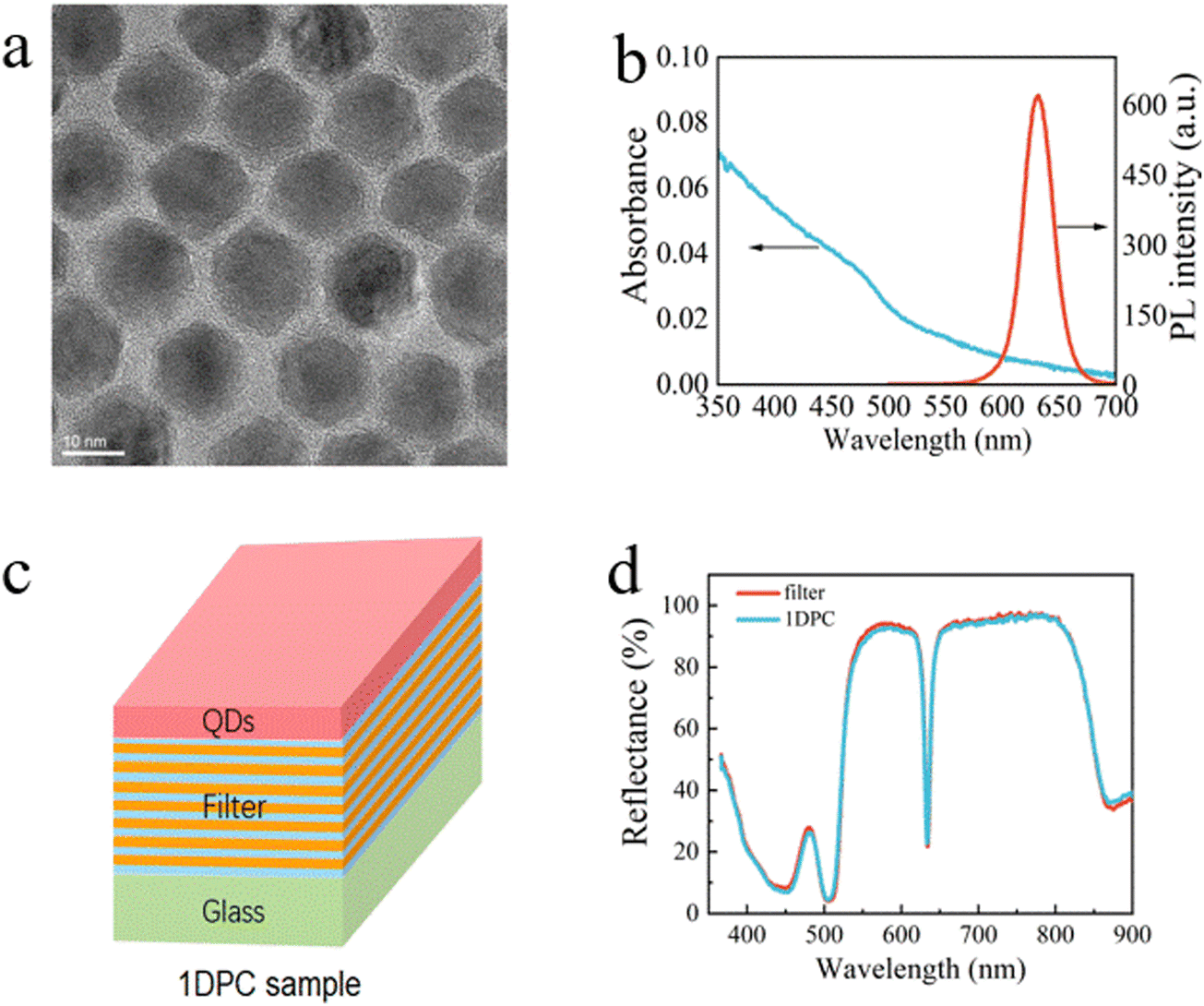 | ||
| Fig. 1 (a) TEM of CQD; (b) Abs and PL spectra of the CQD film; (c) schematic structure of the 1DPC sample 1; (d) reflectance spectra of the filter 1 and 1DPC CQD sample 1. | ||
To investigate the influence of the defect mode of the filter on the luminescent properties of the CQD film, we conducted measurements and compared the PL spectra of the 1DPC and ref samples at the normal direction using a UV pulse laser at 355 nm, as depicted in Fig. 2(a). (The optical path diagram of the test is shown in Fig. S1, ESI†). In the ref sample 1, the PL emission peak is observed at 634 nm, consistent with previous measurements, and the FWHM is 32.4 nm. The 1DPC sample 1 exhibits a PL emission peak at 637 nm with a significantly reduced FWHM of 16.5 nm. The spectrum of the 1DPC sample 1 is narrowed significantly, and the intensity is increased threefold compared to the ref sample. This outcome suggests that the defect mode of the passive filter continues to exert a strong influence on the PL properties of the CQD film, even when the film is not directly located at the position where the defect state mode is formed. Despite the CQD film being on the surface of the filter, and the localized electromagnetic field is much weaker than that of the defect position of the filter, the high PDOS associated with the defect state mode still induces a noticeable Purcell effect, aligning with the principles of cavity quantum electrodynamics.
 | ||
| Fig. 2 (a) Comparison of PL spectra of the 1DPC and ref samples; (b) variable angle PL spectra of the ref sample 1; (c) variable angle PL spectra of the 1DPC sample 1; (d) fluorescence lifetimes of the 1DPC and ref samples. | ||
In Fig. 2(b), the variable-angle PL spectra of the ref sample 1 from 0° to 70° are depicted. The emission peak position remains constant, while the intensity gradually decreases with an increasing detection angle. This phenomenon indicates that the ref sample 1 can be regarded as a Lambertian emitter, the emission from spontaneous radiation is isotropic, and the peak wavelength does not vary with the viewing angle. In Fig. 2(c), the variable-angle PL spectrum of the 1DPC sample 1 shows a gradual blue shift in emission peaks and decreasing peak intensity as the angle continues to change. This behavior aligns with a regular defect state modulation mode, as the PDOS of the defect state mode decreases with the increase of the observation angle.
In Fig. 2, the filter's structure is Glass/[HL]3H2L[HL]2H. There is a 2L defect layer sandwiched between two reflectors. The wavelength λ0 of the defect state mode of the filter is determined by the following Fabry–Perot peak condition:
 | (1) |
In Fig. 2(d), the fluorescence lifetime of the 1DPC sample 1 is measured at 42.84 ns, while that of the ref sample is 54.58 ns, indicating a decrease of 11.74 ns in fluorescence lifetime after the modulation of the filter. The PLQY of the 1DPC and ref samples are 61.5% and 76.3%, respectively. From these values, we deduce that the radiative transition rates of the 1DPC and the ref samples are 1.44 × 10⁷ s−1 and 1.39 × 10⁷ s−1, respectively. This implies that after the modulation effect of the defect state mode of the filter, the PDOS of CQD luminescent layer is increased, leading to an increase in the radiative transition rate and a decrease in the fluorescence lifetime.
To ensure a more accurate evaluation of intensity enhancement, considering the different reflectance of the filter and glass substrate at the excitation wavelength of 355 nm, we utilized a 450 nm laser as the excitation light source. This choice was made because at this wavelength, the reflectance of the 1DPC and the ref samples is nearly identical. Both PL spectra from the front and back sides of the samples in the normal direction were measured. Fig. 3(a) shows the front-side PL spectra of the 1DPC and ref samples. Due to the extended exposure to air, the PL emission peak of the ref sample 1 has shifted to 631 nm, while the PL emission peak of the 1DPC sample 1 is at 636 nm. It is evident that the PL spectrum of the 1DPC sample 1 is modulated by the defect state mode of the filter, resulting in a narrowed spectrum and more than a twofold increase in emission intensity compared to that of the ref sample 1. The backside PL spectra of the two samples are shown in Fig. 3(b). The presence of the filter and its limited light transmission significantly narrows the PL spectrum of the 1DPC sample 1 on the backside. However, the PL peak intensity of the 1DPC sample 1 is slightly lower than that of the ref sample 1. These findings indicate that the PL emission of the 1DPC sample 1 is subject to the Purcell effect on the front side, while the primary influences on the backside are due to the optical filtering effect.
 | ||
| Fig. 3 PL spectra of the 1DPC and the ref samples in, (a) surface normal direction; (b) back normal direction. (c) Photon density of states and (d) modelled spectra for ref and 1DPC samples. | ||
As shown in Fig. 3(c) and (d), transfer-matrix method was utilized to model the PDOS and the PL spectrum of the two samples.18 In the modeled results, it is observed that the PDOS of the ref sample 1 remains almost constant within the range of the PL spectrum. While, the 1DPC sample 1 exhibits a narrow band PDOS with a peak intensity enhanced approximately 7 times compared to the value of the ref sample 1. Given that the CQD luminescent film is situated at the outermost layer of the sample, the 1DPC demonstrates weak photon localization at the CQD layer, presenting a similar electric field intensity to that of the ref sample 1. Consequently, the PL emission spectrum is primarily influenced by PDOS, as illustrated in Fig. 3(d). This underscores the conclusion that, even when the light-emitting layer is not at the defect position, it is still regulated by the defect state mode of the 1DPC due to the increased PDOS.
Typically, the regulation of spontaneous emission occurs in a light-emitting defect layer situated within the interior of 1DPCs. Achieving the desired resonant wavelength requires precise control of the thickness of this light-emitting defect layer, and on top of this layer, another multilayer periodic structure is often grown. This process adds complexity to the preparation, limiting the use of certain materials for which controlling film thickness or depositing top multilayers is challenging. In comparison, placing the luminescent material on the surface layer, as opposed to within the interior, simplifies the structure design. Our results demonstrate that luminescent modulation can be achieved by separating the defect layer and luminescent layer. This approach offers an effective means to enhance luminescent properties through a more straightforward structure design and preparation, greatly facilitating sample preparation.
In order to further explore the effect of the defect state mode of the 1DPC on the ASE properties, a quasi-2D perovskite PEA2FAn−1PbnBr3n+1 (n = 9, P2F9) was applied for further investigation.19Fig. 4(a) shows the Abs and PL spectra of the P2F9 film. There is an absorption peak at 500 nm and a PL emission peak at 536 nm, with FWHM measurement of approximately 30 nm.
 | ||
| Fig. 4 (a) Abs and PL spectra of the P2F9 film; (b) transmittance spectra of the filter 2 and 1DPC sample 2. | ||
Similarly, the transmission peak of the designed filter 2 is close to the PL peak position of the P2F9 film. The structure of the filter 2 is Glass/[HL]5H2L[HL]4H, where H is a 58.8 nm-thick high refractive index material of TiO2 (refractive index of 2.29) and 92.7 nm-thick low refractive index material of SiO2 (refractive index of 1.46). Fig. 4(b) shows the transmission spectrum of the filter 2, which has a defect mode at 540 nm. After that the P2F9 film is spin-coated on the top of the filter 2, the defect state mode slightly blue shifts to the 536 nm. The measured defect state mode is in agreement with the simulation results by the transmission matrix method (Fig. S2, ESI†). In comparison to the almost identical reflection spectra of 1DPC sample 1 and its filter, there is a big difference in the transmittance spectra between the 1DPC sample 2 and filter 2. This is due to differences in thickness and absorption of luminescent layers. The CQD film used in 1DPC sample 1 is very thin (∼20 nm) and has a weak absorption. However, the P2F9 film used in 1DPC sample 2 is much thicker (∼100 nm) and has a strong absorption at the UV and blue spectral region. Therefore, the curve difference in Fig. 4(b) is big.
In order to study the influence of the defect state mode of filters on the surface emission ASE properties of P2F9 film, a 355 nm UV pulse laser was used as the excitation light source. By using a neutral density filter to adjust the energy of the pump laser, PL spectra of the 1DPC samples and its reference sample under different pump fluence were obtained. Fig. 5(a) shows the changes in the emission spectrum of reference sample 2 (Glass/P2F9) under pump fluence of 10 μJ cm−2–70 μJ cm−2. Fig. 5(b) shows the relationship between the PL intensity and FWHM of reference sample 2 under different pump fluence. As the pump intensity increases, the PL spectrum intensity increases, and the fluorescence peak is located at 532 nm. When the pump fluence exceeds 61.97 μJ cm−2, the emission intensity begins to increase nonlinearly, and a narrow and strong peak appears at 540 nm. Emission spectrum with fluorescence and ASE peaks of reference sample 2 is shown in Fig. S3 (ESI†). At this time, the spontaneous emission of the P2F9 film begins to change into amplified spontaneous emission, which is the ASE phenomenon. With the nonlinear enhancement of fluorescence intensity, the FWHM of PL decreased from 27.9 nm to 3.6 nm. Fig. 5(c) shows the emission spectra of the 1DPC sample 2 (Glass/filter 2/P2F9) as a function of pump fluence, and Fig. 5(d) shows the vary of the PL intensity and FWHM of 1DPC sample 2 with the pump intensity. At low pump fluence, except for an emission peak at 532 nm, there is also an emission peak at 540 nm originated from the defect state mode of the filter. As the pump fluence increases, 540 nm emission peak becomes stronger gradually (Fig. S4, ESI†), while the FWHM of PL decreased from 27.8 nm to 4.1 nm, indicating the occurring of the ASE phenomenon. The 1DPC sample 2 shows a lower pump threshold (Pth) of 50.92 μJ cm−2 compared to that of the reference sample 2 (61.97 μJ cm−2). It can be calculated that the filter defect state reduces the ASE threshold of the P2F9 film by about 17.8%.
 | ||
| Fig. 5 Emission spectra of (a) reference sample 2, (c) 1DPC sample 2 and (e) 1DPC sample 3 under different pump fluence; The PL intensity and FWHM of (b) reference sample 2, (d) 1DPC sample 2 and (f) 1DPC sample 3 as a function of the pump fluence. | ||
To further explore the effect of the filter defect state mode on P2F9 film, the 1DPC sample 3 with the filter defect state mode at 555 nm was prepared, in which the defect state mode deviates the peak position of ASE. Fig. 5(e) shows the emission spectra of the 1DPC sample 3 under different pump fluence. Under low pump fluence, in addition to the original fluorescence peak of 532 nm, there is also a fluorescence peak at the filter defect state mode position of 555 nm (Fig. S5, ESI†). As the pump fluence increases, the ASE peak at 539.6 nm begins to appear, but the filter defect state mode peak at 555 nm still exists. Fig. 5(f) shows the PL intensity and FWHM of the 1DPC sample 3 as a function of the pump fluence. As the pump fluence increases, the FWHM decreases from 27.1 nm to 3.5 nm, and the ASE Pth of this sample is 69.80 μJ cm−2. The Pth of ASE increased by 12.64% compared to that of the reference sample 2 (61.97 μJ cm−2). The increased Pth can be attributed to the emission of the filter defect state mode dissipates the pump fluence.
Fig. 6(a) and (c) displays the emission properties of 1DPC sample 3 in the normal direction of the back surface (glass side). The emission spectra were tested under different pump fluence, and the optical path diagram has been shown in Fig. S6 (ESI†). Under low pump energy, there is only one fluorescence peak at 555 nm from the filter defect state mode. As the pump fluence increases, the ASE emission peak gradually emerge and become stronger at 540 nm. Filter defect state mode 555 nm and ASE peak 540 nm are shown in Fig. S7 (ESI†). The FWHM of the ASE spectra gradually decreases from 21.6 nm to 4.3 nm, and the threshold of ASE is 79.41 μJ cm−2.
 | ||
| Fig. 6 Emission spectra of 1DPC sample 3 at the back side, (a) in the normal direction, and (b) at viewing angle 24°; the dependence of emission intensity and FWHM of the 1DPC sample 3 on pump fluence, (c) in the normal direction, and (d) at viewing angle 24°. | ||
Generally, the defect state mode of the filter is angle sensitive, which will be blue shift with the probe angle. Based on this property, we calculated that when the observation angle is 24° with the normal direction, the filter mode will blue shift to 540 nm-the peak position of ASE. The reflectance spectra simulated by the transmission matrix method is shown in Fig. S8 (ESI†). Therefore, we placed the fiber probe at this angle and measured the emission properties of 1DPC sample 3, as shown in Fig. 6(b) and (d). It can be seen that there is only one emission peak shown at 540 nm under different pump fluence. The FWHM of the ASE peak decreases from 12.6 nm to 3.7 nm, and the threshold is 70.47 μJ cm−2, which is reduced by approximately 11.25% compared to that of the sample detected at the normal direction. At the same pump fluence, the emission intensity of 1DPC sample 3 modulated by the defect state mode of the filter to the ASE position (24°) is about 3 times higher than that of the unmodulated case (0°) (Fig. S9, ESI†). The results illustrate that the ASE pump threshold can be easily modulated through the filter defect state mode with variable detect angles, verifying the possibility of the filter can be used in laser devices.
Conclusions
In conclusion, our study has explored the modulation of luminescent properties in CdZnSeS-based CQD films through the implementation of a 1DPC filter. The defect state mode of the filter, even when not directly aligned with the luminescent layer, significantly influences the PL characteristics of the CQD film. This is evidenced by a narrowed PL spectrum and a substantial increase in emission intensity. The transfer matrix method was employed to model the PDOS and PL spectra, revealing a sevenfold enhancement in PDOS within the 1DPC sample. Further, we explored the impact of the filter defect state mode on the stimulated emission properties by using a quasi-2D perovskite P2F9 film. When the filter mode is at the ASE peak position of the P2F9 film, it will help to reduce ASE threshold and enhance emission intensity of the P2F9 film. Importantly, this study indicates that the traditional requirement of placing a light-emitting defect layer precisely within the interior of 1DPCs can be circumvented. Placing the luminescent material on the surface layer simplifies the structure design and preparation process. The separated defect layer and luminescent layer approach provides an effective and simplified means to achieve enhanced spontaneous and stimulated emission, making the adjustment of the defect state mode position more convenient and faster, and thus for potential applications in light emitting devices and lasers.Experimental
Materials
ZnSe, YF3, TiO2 and SiO2 were purchased from Beijing Dream Material Technology Co., Ltd, with a purity of 99.99%. The quantum dots material utilized in our study is CdZnSeS/CdZnS/ZnS alloyed red-emitting CQDs, synthesized by Suzhou Xingshuo Nanotech Co., Ltd (Mesolight). PbBr2, PEABr and FABr were purchased from Xi’an Polymer Light Technology Corp. All materials were used directly without further purification.Preparation of optical filter
The first optical filter employed in our experiment comprises a stacked arrangement of high refractive index (H) and low refractive index (L) materials. Specifically, the high refractive index material, denoted as H, is ZnSe, and the low refractive index material, denoted as L, is YF3. Filter 1 has 13 layers with a ZnSe thickness of 61 nm and YF3 thickness of 105 nm. As for the substrates, BK7 glasses were employed. To ensure cleanliness, the substrates underwent ultrasonic cleaning using acetone, ethanol, and deionized water sequentially for 15 min. Subsequently, they were placed in a vacuum drying oven for drying treatment and finally dried under an infrared baking lamp for spare parts. The first filter was prepared through electron beam thermal evaporation method, maintaining a vacuum of 2 × 10⁻³ Pa. The evaporation rates for ZnSe and YF3 were set at 0.2 nm s−1 and 0.4 nm s−1, respectively. While, the 2nd and 3rd optical filters employed TiO2 and SiO2 as H and L materials, respectively. Filter 2 has 21 layers with a TiO2 thickness of 56.4 nm and SiO2 thickness of 92.7 nm. Filter 3 has 21 layers with a TiO2 thickness of 58.2 nm and SiO2 thickness of 95.4 nm. The structure and layer parameter diagrams of the three 1DPC samples are shown in Fig. S10 (ESI†). The TiO2 and SiO2 layers were deposited by electron beam evaporation at a substrate temperature of 200 °C in an oxygen pressure of 2 × 10⁻² Pa with deposition rates of 0.4 and 0.35 nm s−1, respectively.Preparation and characterization of 1DPC samples
1DPC sample has a structure of glass/filter/top luminescent layer, and ref sample has a structure of glass/top luminescent layer. We first explore the impact of 1DPC and defect state on the spontaneous emission properties of the top CQD luminescent film. The CQD films in 1DPC and ref sample 1 were prepared with the same process condition to ensure the consistency of film thickness. Spin coat the CQD solution onto the glass substrate or filter surface at 3000 rpm for 30 s, and then anneal in a nitrogen glove box (H2O < 1 ppm, O2 < 1 PPM) at 90 °C for 10 min. The thickness of the CQD film obtained is approximately 20 nm.We further explore the effect of 1DPC and defect state on the ASE properties of the top P2F9 luminescent film. Here, we change the top luminescent layer material because we found that the CQD film used does not show ASE properties. So we chose the quasi-two-dimensional perovskite material (P2F9) as the luminescent layer, whose ASE phenomenon has been observed before.19 The P2F9 films in 1DPC and reference sample 2 were prepared with the same process condition to ensure the consistency of film thickness. Weigh PEABr, FABr, and PbBr2 materials on an electronic balance according to the stoichiometric ratio of 1![[thin space (1/6-em)]](https://www.rsc.org/images/entities/char_2009.gif) :4.5:4.5, dissolve them in anhydrous N,N-dimethylformamide (DMF), and set the temperature to 50 °C and stirred for 4 h to obtain an P2F9 solution with a PbBr2 material concentration of 0.4 mM.
:4.5:4.5, dissolve them in anhydrous N,N-dimethylformamide (DMF), and set the temperature to 50 °C and stirred for 4 h to obtain an P2F9 solution with a PbBr2 material concentration of 0.4 mM.
Take 100 μL of P2F9 solution and spin-coat it on the surface of the BK7 glass substrate or filter at 4500 rpm for 30 s. At the 5th second, drop 0.2 mL of ethyl acetate onto the P2F9 film being spin-coated. Then anneal in a nitrogen glove box at 120 °C for 10 min (H2O < 1 ppm, O2 < 1 ppm). The excitation spectra of P2F9 film and CQD film are shown in Fig. S11 (ESI†).
To analyze the optical properties, absorption and PL spectra of the CQD films were obtained using a Shimadzu UV-3101PC UV-Vis spectrophotometer and a Hitachi F-7000 fluorescence spectrometer, respectively. The PL spectra of both 1DPC and ref samples were measured using an Avantes ULS2048L fiber optic spectrometer at a detecting distance of approximately 15 mm in the normal direction of the samples. Two excitation sources were utilized: a CryLas GmbH Nd:YAG pulse laser at 355 nm with a pulse width of 1 ns and a repetition rate of 50 Hz, and a 450 nm CW laser. The detection angle was varied by rotating the sample stage. For fluorescence lifetime analysis, an Edinburgh FLSP920 model fluorescence spectrometer was employed. Reflectance spectra of the samples were measured using an Avantes ULS2048L Fiber Optic Spectrometer.
Conflicts of interest
There are no conflicts to declare.Acknowledgements
This work was supported by the National Natural Science Foundation of China No. 62035013, 51973208, 52211530094, 62175235, 61975256, and the Jilin Province Science and Technology Research Project (20220201064GX, 20220201091GX).References
- S. John, Phys. Rev. Lett., 1987, 58, 2486–2489 CrossRef CAS PubMed.
- E. Yablonovitch, Phys. Rev. Lett., 1987, 58, 2059–2062 CrossRef CAS PubMed.
- L. Zhang, Z. Qi and H. Ma, L. O. P., 2022, 33, 356–363 Search PubMed.
- B. Chen, C. L. Liu and G. Z. Liu, Opt. Commun., 2012, 285, 5100–5106 CrossRef CAS.
- T. W. Lu, C. C. Wu and P. T. Lee, ACS Photonics, 2018, 5, 2767–2772 CrossRef CAS.
- R. Li, L. Li, B. Wang and L. Yu, Nanomaterials, 2021, 11, 3126 CrossRef CAS PubMed.
- T. Li, G. Liu, H. Kong, G. Yang, G. Wei and X. Zhou, Coordin. Chem. Rev., 2023, 475, 214909 CrossRef CAS.
- M. Suzuki, J. Soc. Inf. Disp., 2011, 19, 590–596 CrossRef CAS.
- J. P. Dowling, M. Scalora, M. J. Bloemer and C. M. Bowden, J. Appl. Phys., 1994, 75, 1896–1899 CrossRef CAS.
- J. Tian, Q. Y. Tan, Y. Wang, Y. Yang, G. Yuan, G. Adamo and C. Soci, Nat. Commun., 2023, 14, 1433 CrossRef CAS PubMed.
- D. P. Puzzo, F. Scotognella, M. Zavelani-Rossi, M. Sebastian, A. J. Lough, I. Manners, G. Lanzani, R. Tubino and G. A. Ozin, Nano Lett., 2009, 9, 4273–4278 CrossRef CAS PubMed.
- J. Jasieniak, C. Sada, A. Chiasera, M. Ferrari, Al Martucci and P. Mulvaney, Adv. Funct. Mater., 2008, 18, 3772–3779 CrossRef CAS.
- S. Noda, M. Fujita and T. Asano, Nat. Photonics, 2007, 1, 449–458 CrossRef CAS.
- X. Gao, M. Cathelinaud, X. Zhang, H. Ma and Z. Liu, Opt. Mater., 2022, 130, 112587 CrossRef CAS.
- L. Wang, J. Lin, Y. Lv, B. Zou, J. Zhao and X. Liu, ACS Appl. Nano Mater., 2020, 3, 5301–5310 CrossRef CAS.
- H. Chang, Y. Zhong, H. Dong, Z. Wang, W. Xie, A. Pan and L. Zhang, Light: Sci. Appl., 2021, 10, 60 CrossRef CAS PubMed.
- G. Rainò, N. Yazdani, S. C. Boehme, M. Kober-Czerny, C. Zhu, F. Krieg, M. D. Rossell, R. Erni, V. Wood, I. Infante and M. V. Kovalenko, Nat. Commun., 2022, 13, 2587 CrossRef PubMed.
- M. D. Tocci and M. Scalora, Phys. Rev. A, 1996, 53, 2799–2803 CrossRef CAS PubMed.
- D. Zou, Y. Wang, Y. Zhang, X. Guo, Y. Lv, J. Lin, J. Huang and X. Liu, J. Mater. Chem. C, 2023, 11, 11730 RSC.
Footnote |
| † Electronic supplementary information (ESI) available. See DOI: https://doi.org/10.1039/d4tc00181h |
| This journal is © The Royal Society of Chemistry 2024 |