
 Open Access Article
 This Open Access Article is licensed under a
 Creative Commons Attribution 3.0 Unported Licence
Unveiling the stacking-dependent electronic properties of the 2D ultrathin rare-earth metalloxenes family LnX2 (Ln = Eu, Gd, Dy; X = Ge, Si)†
Alexey N.
Mihalyuk
 *ab,
Polina M.
Sheverdyaeva
*c,
Jyh-Pin
Chou
d,
Andrey V.
Matetskiy
c,
Sergey V.
Eremeev
e,
Andrey V.
Zotov
b and
Alexander A.
Saranin
b
*ab,
Polina M.
Sheverdyaeva
*c,
Jyh-Pin
Chou
d,
Andrey V.
Matetskiy
c,
Sergey V.
Eremeev
e,
Andrey V.
Zotov
b and
Alexander A.
Saranin
b
aInstitute of High Technologies and Advanced Materials, Far Eastern Federal University, 690950 Vladivostok, Russia. E-mail: mih-alexey@yandex.ru
bInstitute of Automation and Control Processes FEB RAS, 690041 Vladivostok, Russia
cIstituto di Struttura della Materia-CNR (ISM-CNR), Strada Statale 14 km 163.5, 34149 Trieste, Italy. E-mail: polina.sheverdyaeva@ism.cnr.it
dDepartment of Physics, National Changhua University of Education, No. 1, Jinde Rd., Changhua City, Changhua County 50007, Taiwan
eInstitute of Strength Physics and Materials Science, Tomsk 634055, Russia
First published on 26th March 2024
Abstract
Studies of electronic effects in reduced dimensionality have become a frontier in nanoscience due to the exotic and highly tunable character of quantum phenomena. Recently, a new class of 2D ultrathin LnX2 metalloxenes composed of a triangular lattice of lanthanide ions (Ln) coupled with 2D-Xenes of silicene or germanene (X2) was introduced and studied with a particular focus on magnetic and transport properties. However, the electronic properties of metalloxenes and their effective functionalization remain mainly unexplored. Here, using a number of experimental and theoretical techniques, we trace the evolution of the electronic properties and magnetic ground state of metalloxenes triggered by external perturbations. We demonstrate that the band structure of LnX2 films can be uniquely modified by controlling the Xenes stacking, thickness, varying the rare-earth and host elements, and applying an external electric field. Our findings suggest new pathways to manipulate the electronic properties of 2D rare-earth magnets that can be adjusted for spintronics applications.
1. Introduction
The family of low-dimensional materials that have 2D intrinsic magnetism has been growing impressively in recent years, expanding the scope of possible phenomena to be explored in 2D and enabling the development of novel devices.1–3 Like graphene and transition-metal dichalcogenides revolutionized materials engineering, the discovery of 2D atomic magnets opened up numerous opportunities for applications and fundamental research. Rare earth metalloxenes (LnX2) is a class of layered materials where honeycomb-like layers of semiconductor (Ge or Si) are separated by layers of rare-earth atoms of lanthanide series (Ln).4–10 The layered character, availability of epitaxial growth on semiconducting substrates and a variety of lanthanide elements make LnX2 a playground for studying the magnetism and transport in ultrathin film limit. Indeed, these systems demonstrated fingerprints of strong 2D ferromagnetic (FM) ordering in the monolayer (ML) limit,11 together with high carrier mobility,12 non-trivial topology13 and remarkable transport phenomena.14 The electronic band structures of some LnX2 films were investigated through angle resolved photoemission spectroscopy (ARPES)15–20 and density functional theory (DFT) studies.10,20,21 However, a systematic study treating the electronic properties of these films as a function of thickness, Ln and host X element is still missing. The electronic and magnetic properties of LnX2 films are furthermore expected to be sensitive to external perturbations, such as strain, charge doping and electric field.22 In particular, surface doping of the films can significantly alter the electronic and structural properties of thin films, changing their electronic and magnetic properties.23 Recently, a pure antiferromagnetic (AFM) order was found for in situ grown LnX210 films, as compared to FM order fingerprints observed in SiOx capped ones.24–26In this work, we carry out a combined experimental and theoretical study to investigate the structure as well as the electronic and magnetic properties of the LnX2 (Ln = Eu, Gd, Dy; X = Ge, Si) family, and the effect of interface modification on it. The structure of the in situ grown, or pristine films is found by comparing the DFT calculations to the ARPES data, while the structure of the capped LnX2 films is revealed from previously published high-angle annular dark-field transmission electron microscopy (HAADF-TEM) studies.4,27 We discuss similarities and differences in the electronic structure of LnX2. We discovered that depending on the lanthanide and host elements, a capping layer is capable of triggering significant changes in the structure, electronic properties and magnetic anisotropy. We furthermore analysed the effect of an external electric field and found that it can effectively tune the position of the Fermi level. Our study offers insights into the electronic properties of 2D ultrathin rare-earth LnX2 films and their effective functionalization.
2. Experimental and calculation details
Samples growth
Ge(111) and Si(111) substrates were used for the in situ growth of the LnX2 films. Ge(111) substrates were sputtered with Ar+ ion bombardment and then annealed at 650 °C; this procedure was repeated several times until the appearance of a sharp c(2× 8) low-energy electron diffraction (LEED) pattern. To prepare the Si(111)-7 × 7 surface reconstruction, the Si(111) sample was flash annealed to a temperature of ∼1200 °C. Lanthanide elements were deposited using electron bombardment sources with rates of ∼ 0.25 ML min−1. The evaporation rate was calibrated by observation of LEED patterns that correspond to known surface reconstructions: 5 × 2 at a coverage less than 1 ML, 1 × 1 that corresponds to the completion of the first ML at a coverage of ∼1 ML and at a coverage above 1 ML (ESI,† Section S1).28 During deposition, the substrates were held at ∼400 °C. In the case of Si-based metalloxenes, samples were also annealed at ∼550–650 °C to improve the crystalline quality of the films. It should be noted that this procedure produces films with multiple film thicknesses after 1 ML completion.28,29
ARPES measurements
The experiments were carried out at the VUV-photoemission beamline at Elettra synchrotron (Trieste, Italy), using angle-resolved photoelectron spectroscopy (ARPES). The base pressure of the analytic and preparation chambers was ≤1.0 × 10⁻¹⁰ Torr and ≤3 × 10⁻¹⁰ Torr, respectively. The majority of ARPES measurements were carried out at a temperature of 14 K using a Scienta R4000 electron analyzer and 35 eV photon energy, which allowed for the best contrast of the features of interest. The electron spectrometer was placed at 45° with reference to the direction of the incoming p-polarized photon beam. The labels of the high-symmetry points in the ARPES spectra refer to the 1 × 1 surface Brillouin zone (SBZ).DFT calculations
The calculations were based on density-functional theory (DFT) as implemented in the Vienna Ab initio Simulation Package VASP.30 The projector-augmented wave approach31 was used to describe the electron–ion interaction. The generalized gradient approximation (GGA) of Perdew, Burke, and Ernzerhof (PBE) was used as the exchange–correlation functional for structural optimization. The spin–orbit coupling (SOC) was taken into account.To simulate the LnX2 structures, we used a germanium/silicon slab with PBE-optimized bulk lattice constants. Hydrogen atoms were used to passivate the dangling bonds at the bottom of the slab. The kinetic cutoff energy was 250 eV and 12 × 12 × 1 and 7 × 7 × 1 k-point meshes were used to sample the 1 × 1 and  2D Brillouin zones, respectively. Geometry optimization was performed until the residual force on the atoms was less than 10 meV Å−1. The Heyd–Scuseria–Ernzerhof (HSE06) screened hybrid functional32 was used to calculate the band structure. Two types of Ln pseudopotentials were used:33 in non-magnetic calculations the potentials where valence 4f electrons are treated as core states; while to describe the magnetic properties, standard Ln potentials were utilized. Since the Gd-based metalloxenes were the main focus of the study, we performed a low-temperature ARPES measurement (14 K) of a thick (20 ML) GdGe2 film to provide experimental evidence for the Gd-f band position. As follows from Fig. S2(a) (ESI,† Section S2), a strongly localized f-band is located at ∼−8.5 eV. This observation is in line with the trivalent state of Gd34 and was used to verify the accuracy of the HSE06 hybrid functional in the description of the electronic spectra.
Ab initio random structure searching (AIRSS) method
In the present study, we use the ab initio random structure searching (AIRSS) method, which is a straightforward and powerful approach toward structure prediction, based on the stochastic generation of sensible initial structures and their repeated local optimization.35 The initial random structures are generated to broadly sample a subvolume of the total configuration space.36 This subvolume is defined by the search parameters, such as the range of unit cell volumes and shapes, species-dependent minimum distances, structural or molecular units, and symmetry. The details on the implementation of the AIRSS method for the search for the ground state model of the 2 ML GdGe2 film are given in the ESI,† Section S3 as an example.3. Results and discussion
3.1. Atomic structure of LnX2 metalloxenes: the geometry, stoichiometry and stacking type
The basic building block of the LnX2 metalloxene as follows from HAADF-TEM observations27 is a triangular lattice of lanthanide ions coupled with honeycomb networks of host Si(Ge) atoms. To theoretically interpret the experimentally observed atomic ordering of the LnX2 films, we employed the AIRSS method35 (more details are given in the ESI,† Section S3) and independently found ground-state models for films of 1 ML and 2 ML thickness. Calculations for EuGe2 show that Eu atoms of the first and second layers prefer to stay at the H3 site in reference to the underlying Ge(111) substrate, while the geometry of the segregated buckled honeycomb Ge atomic sheet is the following: the upper Ge atom stays at the T1 site, while the lower Ge atom is located at the T4 site (Fig. 1(a)). As regards the 2 ML EuGe2 system, the most energetically stable model has the same arrangement as the 1 ML system: the subsequent Eu and Ge atomic layers keep the same positions with respect to the former ones (Fig. 1(b)). As a result, the Eu atoms are always centered in the hole of the honeycomb lattice of the lying above Ge bilayer, as shown in the top and side views in Fig. 1(a) and (b). As found, all theoretical findings appear to perfectly follow the HAADF-TEM observations for EuGe227 shown as the underlying images in Fig. 1(a) and (b). This agreement confirms the validity of the AIRSS method and the accuracy of the implemented density-functional theory (DFT) calculation scheme. It should be noted that for the HAADF-TEM measurements, the samples were preliminary covered with a SiOx capping layer of 20 nm thickness.27 However, excellent agreement in the structure between calculation and experiment allows us to conclude that capping does not affect the EuGe2 film atomic stacking. | ||
Fig. 1 Stacking-dependent ground-state structural models of the EuGe2 (a) and (b), GdGe2 (c) and (d) and GdSi2 (e) and (f) films of various thicknesses. Black dashed rhombi outline the 1 × 1 (a)–(c) and (e) and  (d) and (f) unit cells. The observation of the stacking order under the capping layer (a)–(d) is provided by TEM images reproduced from ref. 27 with permission from the Royal Society of Chemistry, and the TEM images in (e) and (f) were reproduced from ref. 4 with permission from Elsevier Ltd. (d) and (f) unit cells. The observation of the stacking order under the capping layer (a)–(d) is provided by TEM images reproduced from ref. 27 with permission from the Royal Society of Chemistry, and the TEM images in (e) and (f) were reproduced from ref. 4 with permission from Elsevier Ltd. | ||
Let us now examine the case of GdGe2 films. Fig. 1(c) shows the ground-state atomic model of the 1 ML film with stacking order as obtained from the AIRSS method; here, the Gd atom, in contrast to Eu, has a different adsorption position – T4 one instead of the H3 site for Eu. Next, the geometry of the topmost buckled honeycomb Ge atomic sheet is also different: the upper Ge atom is located at the T1 site (which is the same as in the EuGe2 case), but the lower Ge atom is now located at the H3 site (instead of the T4 site in the EuGe2 case).10 However, the Gd atoms are positioned at the centers of the honeycomb buckled germanene lattice, like in the case of Eu, which is seen in the top-view atomic model (Fig. 1(c)). The structure has 1 × 1 periodicity, which follows from the LEED pattern measured for the pristine film under ultra-high vacuum conditions (ESI,† Section S1). Now, if we turn to the HAADF-TEM observations27 of the 1 ML GdGe2 sample covered by the capping layer, we may see perfect agreement for the position of the Gd atom; however, the stacking of the upper Ge bilayer is different. As follows from the TEM image, the upper Ge atom is located just above the Gd atom at the T4 site, while the lower Ge atom stays at the T1 site, both different from those in the AIRSS-derived ground state model. So, one may conclude on the presence of a lateral shift or sliding of the Ge bilayer relative to the underlying Gd layer. The total energy of the model constructed from the TEM data is by ≈1 eV per unit cell higher than that of the ground-state model (see the ESI,† Section S3 for more details). The top-view ball-and-stick atomic model placed just below the HAADF-TEM image in Fig. 1(c) additionally illustrates capping-induced stacking, where one may see that the Gd atoms are located just below one of the Ge sites, but not in the honeycomb centers. It is worth noting that the SiOx capping layer was omitted from considerations in our DFT band structure calculations for the following reasons: SiOx is a wide-gap insulator, whose states do not overlap with the LnX2 spectral features of interest; SiOx is an amorphous phase24 and cannot be directly simulated in DFT; and finally, according to a previous report,4 the chemical reaction between SiOx and LnX2 is unlikely. Therefore, the study of the mechanisms underlying the capping-induced changes of the stacking is out of the focus of the present paper. From a thermodynamic perspective, the GdGe2 film with pristine stacking order is self-sustainable, but the model derived from the TEM observation shows instability (see the phonon calculations in the ESI,† Section S4). Nevertheless, in the presence of a capping layer, the structure becomes stable, as demonstrated in the HAADF-TEM experiments.4,27 It is known that an elimination of the observed soft phonon mode can be achieved by a tensile strain37,38 induced by the capping layer or doping. There is evidence of interface modification due to the presence of a capping layer despite the fact that the new interface geometry is energetically unfavorable compared to the pristine one.39
It is known that the formation of GdGe2 films thicker than 1 ML reduces the symmetry of the surface from 1 × 1 to  ,29 as demonstrated by the emergence of weak
  reflexes in the LEED pattern (ESI,† Section S1). The distinctive feature of multilayer GdGe2 films is the flat intermediate Ge monolayer where the buckling is removed due to the formation of a vacancy.15Fig. 1(d) shows the calculated 2 ML ground state model, where the intermediate flat Ge ML is marked by red balls, while the vacancies are highlighted by red triangles. The stacking order at the interface between the upper Ge-BL and Gd layers here is the same as in the case of the 1 ML GdGe2 film. As follows from the TEM image, capping the 2 ML GdGe2 sample induces the formation of a different stacking order for the upper Ge-BL (Fig. 1(d)), alike in the 1 ML GdGe2 film. However, the positions of the Gd atoms and the atoms of the intermediate flat Ge ML are identical in both films: capped by a protective layer and the pristine one.
The structure of the GdSi2 system is almost identical to GdGe2 ((Fig. 1(e) and (f)), see also the LEED data in the ESI,† Fig. S1(c) and (d) and Section S1) and the capping-induced stacking order is also less favorable than the pristine ground state (by 0.66 eV). Regarding the DyGe2 system, there is no available HAADF-TEM observation here; nevertheless, DFT calculations (ESI,† Section S5) and ARPES measurements (Fig. 3(e) and (f)) suggest that the arrangement of Dy layers and the Ge-BL stacking order are identical to the GdGe2 case.
3.2. Stacking- and thickness-dependent band structure of the LnX2 metalloxenes family
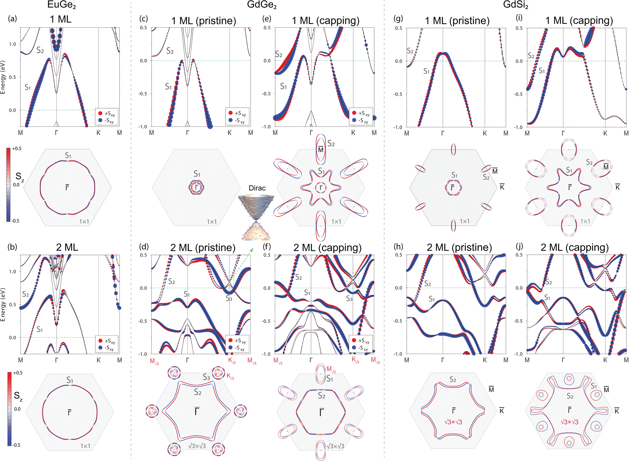
Let us now consider the electronic properties of EuGe2 films, whose structure does not experience any changes induced by the capping layer. Fig. 2(a) shows the spin-resolved relativistic electronic spectrum of the 1 ML EuGe2 film in the non-magnetic case. The distinctive feature of the spectrum is the highly dispersing in-gap S1 hole-like metallic band that possesses small Rashba-type spin splitting and demonstrates hybridization with the Ge(111) conduction band at the![[capital Gamma, Greek, macron]](https://www.rsc.org/images/entities/i_char_e0ba.gif) point. Another distinctive feature is an almost degenerate unoccupied in-gap S2 band with electron-like dispersion at the
point. Another distinctive feature is an almost degenerate unoccupied in-gap S2 band with electron-like dispersion at the ![[M with combining macron]](https://www.rsc.org/images/entities/i_char_004d_0304.gif) point. The Fermi-surface map shows a -centered almost isotropic hole pocket that demonstrates insignificant spin splitting. The spectrum of the 2 ML EuGe2 film (Fig. 2(b)) has very similar features – the S1 band (which intersection with the Fermi level (EF) produces a pair of circular contours) and the parabolic S2 in-gap band dispersing by 0.5 eV above EF. In general, the 1 ML and 2 ML EuGe2 films belong to the class of p-type metals.
point. The Fermi-surface map shows a -centered almost isotropic hole pocket that demonstrates insignificant spin splitting. The spectrum of the 2 ML EuGe2 film (Fig. 2(b)) has very similar features – the S1 band (which intersection with the Fermi level (EF) produces a pair of circular contours) and the parabolic S2 in-gap band dispersing by 0.5 eV above EF. In general, the 1 ML and 2 ML EuGe2 films belong to the class of p-type metals.
 | ||
| Fig. 2 Spin-resolved electronic spectra and Fermi-contour maps calculated for (a) and (b) EuGe2, (c)–(f) GdGe2 and (g)–(j) GdSi2 films of various thickness and stacking type. Red and blue in the electronic spectra and Fermi maps represent opposite in-plane and out-of-plane components of the spin expectation values, respectively, while the balls' size reflects the magnitude of the spins. The highlighted hexagons denote the first Brillouin zone. The image above (d) shows an enlarged view of the Dirac-like cones in the unoccupied spectrum. | ||
Fig. 2(c) shows the DFT calculated band structure of the 1 ML GdGe2 film with pristine stacking, and at first glance it has a very similar character to its EuGe2 counterpart, namely two in-gap bands, the S1 highly-dispersing metallic state and fully unoccupied S2 band. However, the position of the Fermi level here is 0.75 eV higher than in the EuGe2 case and is pinned just at the minimum of the Ge bulk conduction band. As follows from Fig. 2(c) the Fermi surface map has a tiny hole-like pocket produced by the S1 band and even a much smaller electron-like pocket produced by the bulk states, which all characterize the system as a compensated weak metal. Fig. 2(e) shows the spectrum of the GdGe2 film with staking corresponding to the structure with a capping layer. As one can see, the change in stacking order produces drastic changes in the band structure. The most appealing effect is the significant enhancement of the electron density around the Fermi level, provided by the S2 electron band that forms elongated -centered electron pockets with significant Rashba spin splitting in the – direction. The Fermi level position was also changed, and now it is placed within the Ge bulk gap. One may see that capping-induced changes in the atomic structure significantly enrich the electronic properties of the 1 ML GdGe2, which becomes a compensated metal with dominant n-type charge carriers.
Let us now consider the electronic spectra of the 2 ML GdGe2 films with pristine and capping-induced geometry shown in Fig. 2(d) and (f), respectively. In contrast to the EuGe2 case the band structure of the 2 ML GdGe2 film substantially differs from that of the single layer. In the case of a pristine film, the Fermi level is placed exactly in the middle of the Ge bulk gap, whereas S2 and S3 metallic bands form -centered and ![[K with combining macron]](https://www.rsc.org/images/entities/i_char_004b_0304.gif) -centered pockets, respectively, with more noticeable spin splitting compared to the 1 ML film. One may see that the capping-modified interface experiences substantial changes in the electronic spectrum: the S1 band becomes metallic and forms a pair of -centered hole-like pockets, while the S3 band does not produce any pockets at EF due to the hybridization gap. It should be noted that application of a positive perpendicular electric field to the GdGe2 system can easily move the S1 spin-split band at the Fermi level and increase the density of states at EF (see the ESI,† Section S6).
-centered pockets, respectively, with more noticeable spin splitting compared to the 1 ML film. One may see that the capping-modified interface experiences substantial changes in the electronic spectrum: the S1 band becomes metallic and forms a pair of -centered hole-like pockets, while the S3 band does not produce any pockets at EF due to the hybridization gap. It should be noted that application of a positive perpendicular electric field to the GdGe2 system can easily move the S1 spin-split band at the Fermi level and increase the density of states at EF (see the ESI,† Section S6).
Now, we trace the effect of lanthanide and host element variation on the electronic properties of LnX2 films. Section S5 in the ESI† summarizes the results for DyGe2 films, whose atomic and electronic band structure are almost identical to those of GdGe2. Fig. 2(g–j) shows the results for 1 ML and 2 ML GdSi2 films that show a stronger energy overlap between the states at and at as compared to GdGe2. In the Fermi surface, this results in an appearance of additional pockets at for 1 ML and the absence of circular features at for 2 ML, characterizing 1 ML and 2 ML films in the pristine case as compensated and p-type metals, respectively. The band structure for the capped 1 ML GdSi2 is similar to the 1 ML GdGe2 case appearance with the Fermi surface that consists of a star-like hole pocket at the point and elongated pockets in points. In the case of the capped 2 ML GdSi2 film the hybridization effects distort the S2 band and lead to a doubling of the -centered pocket. Interestingly, the pristine and capped 2 ML GdGe(Si)2 films demonstrate a Dirac-like cone at the point just above the Fermi level (shown as the outset above panel (d)), which is a typical feature of a 2D-Xene honeycomb material. We furthermore experimentally probed the band structure for the pristine 1 ML and 2 ML films. Fig. 3(a–f) compare the ARPES observations for the pristine GdGe2, GdSi2 and DyGe2 films to the DFT calculations. The overlap with the calculated states demonstrates that the data are in very good agreement with the DFT predictions for pristine films (see also ref. 10), confirming that the in situ grown films have a different atomic structure as compared to the SiOx-capped ones.
 | ||
| Fig. 3 ARPES spectra for 1 ML and 2 ML GdGe2 (a) and (b), GdSi2 (c) and (d) and DyGe2 (e) and (f) films recorded within 1 × 1 SBZ. All spectra are measured with 35 eV photon energy, at a temperature of 80 K, which corresponds to a non-magnetic phase. The ARPES data demonstrate the spectral characteristics that nicely correspond to the predicted band structures discussed in the main text. (g) and (h) Second derivatives of the ARPES electronic spectra of the 2 ML GdGe2 film recorded in the vicinity of point at temperatures of 14 K and 82 K, respectively, corresponding to the paramagnetic and magnetic phases. The schematic spin-polarized bands are overlaid on the experimental data to demonstrate the change of the spectrum with temperature (which is in line with ref. 10). The red and blue balls represent the opposite in-plane spin components. | ||
3.3. Stacking-dependent magnetic order in LnX2 metalloxenes
The profound effect of the atomic layers stacking on the band structure dispersion (Fig. 2) and orbital character (ESI,† Section S7) of the GdGe(Si)2 films must leave an imprint on the magnetic ground state and consequently on their electronic band structure in the magnetic state. To this aim, first of all, we define the preferred magnetization direction by calculating the total energies for various magnetic configurations (ESI,† Section S8 and Table S1); we found that for 2 ML films the antiferromagnetic in-plane alignment of magnetic moments on Gd atoms of neighboring layers (AFM‖) is the preferred magnetic configuration for both systems. However, for 1 ML films, the preferred magnetization direction in the ferromagnetic (FM) ground state depends on the Ln element and the stacking type: for pristine stacking it is in-plane (FM‖) for GdGe2, whereas it is out-of-plane (FM⊥) for GdSi2. Next, having the preferred magnetic configuration we calculated the band structure. Fig. 4 shows the orbital-resolved and stacking-dependent band structures of the magnetic GdGe2 and GdSi2 films of 1 ML and 2 ML thickness. To trace the dispersion changes, we show the non-magnetic spectra as blue dashed curves. The band structure of the pristine 1 ML GdGe2 film (Fig. 4(a)) demonstrates a noticeable exchange splitting in both the S1 and S2 surface bands, with lifting the degeneracy at the and points. Remarkably, in the case of the capped 1 ML film (Fig. 4(b)) the amplitude of exchange splitting is much larger than in the pristine case. Orbital-symmetry analysis shows that the exchange splitting of S1 and S2 bands comes from Gd f–d hybridization, mediated through the out-of-plane fz3 and dz2 components (shown in Fig. 4 as brown and green circles), which acquire larger weights in the case of the capped film. The exchange splitting in the spectrum of the 2 ML GdGe2 film is rather large in both the pristine and capped cases (Fig. 4(c) and (d)). As for the case of the pristine GdSi2 system (Fig. 4(e)) one may see a significant exchange splitting already at the monolayer limit in contrast to the Ge-based counterpart. However, the capping-induced modification of the film stacking hugely enhances the band splitting, which is again associated with the increased contribution of fz3 orbitals to the S1 and S2 bands (see Fig. 4(f)). Therefore, the study of magnetism-induced effects on the electronic band structure of LnX2 metalloxenes shows the pivotal role of Ln f–d hybridization,40,41 which can be effectively tuned by modification of the interface. The increase in film thickness up to 2 ML leads to a substantial decrease in the exchange splitting in the electronic spectra of the GdSi2 films regardless of the type of stacking due to anti-parallel alignment of the magnetic moments in the neighboring layers (Fig. 4(g) and (h)).
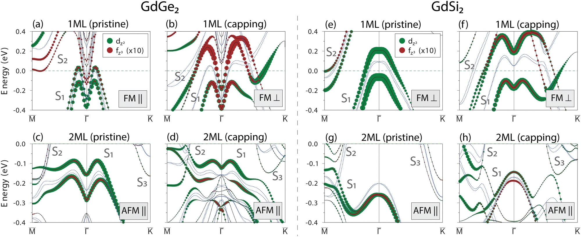 | ||
| Fig. 4 The effect of magnetism on the electronic band structure of GdGe2 (a)–(d) and GdSi2 (e)–(h) films with pristine and capping-induced stacking orders. The spectra demonstrate the contribution of the Gd-d and Gd-f orbitals to the electronic structure. The blue dashed and black solid curves demonstrate the non-magnetic and magnetic spectra, respectively. The preferred magnetic configuration for each system is shown in the panels. | ||
The DFT predictions for the AFM order and the corresponding band splitting in pristine 2 ML GdGe2 films are in line with the ARPES results (ref. 10, Fig. 3(g) and (h)). Due to the lower temperature of the magnetic transition, we were unable to confirm such a splitting in 1 ML GdGe2. Similarly, we were unable to observe any temperature-dependent splitting in other LnX2 systems. Since the EuGe2 films do not experience any stacking modification induced by the capping layer, we give only a short discussion of them (ESI,† Section S8). As regards the case of the EuSi2 and DyGe2 systems, we do not have any HAADF-TEM evidence on the effect of the capping layer and, therefore, leave them out of consideration.
4. Conclusions
In summary, combining the experimental and theoretical techniques we have performed a systematic study of the LnX2 (Ln = Eu, Gd, Dy; X = Ge, Si) family of magnetic metalloxenes in ultrathin film limit (1–2 ML). The structure of the in situ grown films was found by comparing the ab initio random structure searching (AIRSS) method calculations to the LEED data and earlier published HAADF-TEM studies4,27 on the LnX2 films covered by a SiOx capping layer. We have discovered that, depending on the lanthanide and host elements, a capping layer is capable of triggering the change in atomic stacking from a stable to metastable one. In particular, divalent Eu-based and trivalent Gd(Dy)-based metalloxenes generally show three distinctive features of the atomic structure: (1) different positions of the Ln atom with respect to the substrate, H3vs. T4; (2) buckled honeycomb vs. flat intermediate Ge(Si) layers with vacancy; (3) absence of any changes in the X2/Ln interface vs. modification of the interface stacking under the influence of the capping layer. Such structural modifications are capable of producing significant changes in the electronic properties and magnetic anisotropy. The calculated electronic spectra of the stable films that depend on Ln and X elements, as well as on the film thickness, are in perfect agreement with ARPES observations on the pristine LnX2 films in paramagnetic and magnetic state. We furthermore theoretically analyzed the effect of the external electric field and found that it can effectively tune the position of the Fermi level.Thus, our study offers insights into the electronic properties of the 2D ultrathin rare-earth LnX2 films with stable and metastable (realized under capping conditions) atomic structures and suggests ways to control them by variation in Ln and host X elements, film thickness and external electric field for their effective functionalization.
Data availability
Data will be made available on request.Author contributions
A. N. Mihalyuk: software, formal analysis, visualization, conceptualization, writing – original draft, writing – review and editing, project administration. P. M. Sheverdyaeva: investigation, validation, formal analysis, writing – review and editing, resources. Jyh-Pin Chou: software. A. V. Matetskiy: investigation, conceptualization, data curation, writing – review and editing. S. V. Eremeev: software, conceptualization, writing – review and editing. A. V. Zotov: validation. A. A. Saranin: formal analysis. All authors participated in the analysis and discussion of the results.Conflicts of interest
There are no conflicts to declare.Acknowledgements
The electronic band structure calculations and simulations of magnetic properties were supported by the Russian Science Foundation (Grant No. 22-12-00174, https://rscf.ru/project/22-12-00174/). A. V. Matetskiy and P. M. Sheverdyaeva acknowledge EUROFEL-ROADMAP ESFRI of the Italian Ministry of University and Research, and Elettra Sincrotrone Trieste for providing access to its synchrotron radiation facilities (beamtime nr. 20230041). S. V. Eremeev acknowledges the support by the Government research assignment for ISPMS SB RAS, project FWRW-2022-0001. Jyh-Pin Chou acknowledges that the phonon calculations were carried out under financial support from the National Science and Technology Council, Taiwan, ROC (112-2112-M-018-005) and National Center for High-performance Computing (NCHC) of National Applied Research Laboratories (NARLabs) in Taiwan for providing computational and storage resources. The calculations were conducted using the equipment of Shared Resource Center “Far Eastern Computing Resource” IACP FEB RAS (https://cc.dvo.ru).References
- Q. H. Wang, A. Bedoya-Pinto, M. Blei, A. H. Dismukes, A. Hamo, S. Jenkins, M. Koperski, Y. Liu, Q.-C. Sun, E. J. Telford, H. H. Kim, M. Augustin, U. Vool, J.-X. Yin, L. H. Li, A. Falin, C. R. Dean, F. Casanova, R. F. L. Evans, M. Chshiev, A. Mishchenko, C. Petrovic, R. He, L. Zhao, A. W. Tsen, B. D. Gerardot, M. Brotons-Gisbert, Z. Guguchia, X. Roy, S. Tongay, Z. Wang, M. Z. Hasan, J. Wrachtrup, A. Yacoby, A. Fert, S. Parkin, K. S. Novoselov, P. Dai, L. Balicas and E. J. G. Santos, ACS Nano, 2022, 16, 6960–7079 CrossRef CAS PubMed.
- K. S. Burch, D. Mandrus and J.-G. Park, Nature, 2018, 563, 47–52 CrossRef CAS PubMed.
- M. Gibertini, M. Koperski, A. F. Morpurgo and K. S. Novoselov, Nat. Nanotechnol., 2019, 14, 408–419 CrossRef CAS PubMed.
- O. E. Parfenov, A. M. Tokmachev, D. V. Averyanov, I. A. Karateev, I. S. Sokolov, A. N. Taldenkov and V. G. Storchak, Mater. Today, 2019, 29, 20–25 CrossRef CAS.
- I. S. Sokolov, D. V. Averyanov, O. E. Parfenov, I. A. Karateev, A. N. Taldenkov, A. M. Tokmachev and V. G. Storchak, Mater. Horiz., 2020, 7, 1372–1378 RSC.
- D. V. Averyanov, I. S. Sokolov, M. S. Platunov, F. Wilhelm, A. Rogalev, P. Gargiani, M. Valvidares, N. Jaouen, O. E. Parfenov, A. N. Taldenkov, I. A. Karateev, A. M. Tokmachev and V. G. Storchak, Nano Res., 2020, 13, 3396–3402 CrossRef CAS.
- Y. Wang, Z. Cui, H. Zeng, Z. Wang, X. Zhang, J. Shi, T. Cao and X. Fan, J. Mater. Chem. C, 2022, 10, 1259–1269 RSC.
- A. M. Tokmachev, D. V. Averyanov, A. N. Taldenkov, I. S. Sokolov, I. A. Karateev, O. E. Parfenov and V. G. Storchak, ACS Nano, 2021, 15, 12034–12041 CrossRef CAS PubMed.
- D. V. Averyanov, I. S. Sokolov, A. N. Taldenkov, O. E. Parfenov, I. A. Karateev, O. A. Kondratev, A. M. Tokmachev and V. G. Storchak, Nanoscale Horiz., 2023, 8, 803–811 RSC.
- A. V. Matetskiy, V. Milotti, P. M. Sheverdyaeva, P. Moras, C. Carbone and A. N. Mihalyuk, Nanoscale, 2023, 15, 16080–16088 RSC.
- B. Wang, X. Zhang, Y. Zhang, S. Yuan, Y. Guo, S. Dong and J. Wang, Mater. Horiz., 2020, 7, 1623–1630 RSC.
- D. V. Averyanov, I. S. Sokolov, O. E. Parfenov, A. N. Taldenkov, O. A. Kondratev, A. M. Tokmachev and V. G. Storchak, J. Mater. Sci. Technol., 2023, 164, 179–187 CrossRef CAS.
- O. E. Parfenov, D. V. Averyanov, A. M. Tokmachev, I. S. Sokolov, I. A. Karateev, A. N. Taldenkov and V. G. Storchak, Adv. Funct. Mater., 2020, 30, 1910643 CrossRef CAS.
- X. Zhai, R. Wen, X. Zhou, W. Chen, W. Yan, L.-Y. Gong, Y. Pu and X. Li, Phys. Rev. Appl., 2019, 11, 064047 CrossRef CAS.
- P. Wetzel, S. Saintenoy, C. Pirri, D. Bolmont, G. Gewinner, T. P. Roge, F. Palmino, C. Savall and J. C. Labrune, Surf. Sci., 1996, 355, 13–20 CrossRef CAS.
- A. Imai, H. Kakuta, K. Mawatari, A. Harasawa, N. Ueno, T. Okuda and K. Sakamoto, Appl. Surf. Sci., 2009, 256, 1156–1159 CrossRef CAS.
- M. Franz, S. Appelfeller, C. Prohl, J. Grosse, H.-F. Jirschik, V. Fullert, C. Hassenstein, Z. Diemer and M. Dahne, J. Vac. Sci. Technol., A, 2016, 34, 061503 CrossRef.
- C. Rogero, C. Koitzsch, M. E. González, P. Aebi, J. Cerdá and J. A. Martín-Gago, Phys. Rev. B: Condens. Matter Mater. Phys., 2004, 69, 045312 CrossRef.
- C. Koitzsch, M. Bovet, M. Garnier, P. Aebi, C. Rogero and J. Martin-Gago, Surf. Sci., 2004, 566–568, 1047–1051 CrossRef CAS.
- S. Sanna, J. Plaickner, K. Holtgrewe, V. M. Wettig, E. Speiser, S. Chandola and N. Esser, Materials, 2021, 14, 4104 CrossRef CAS PubMed.
- G. Yang, J.-S. Chai, K. Bu, L.-F. Xu and J.-T. Wang, Phys. Chem. Chem. Phys., 2022, 24, 6782–6787 RSC.
- M. Shrivastava and V. Ramgopal Rao, Nano Lett., 2021, 21, 6359–6381 CrossRef CAS PubMed.
- M. Güttler, A. Generalov, M. Otrokov, K. Kummer, K. Kliemt, A. Fedorov, A. Chikina, S. Danzenbächer, S. Schulz and E. V. Chulkov, et al. , Sci. Rep., 2016, 6, 24254 CrossRef PubMed.
- A. M. Tokmachev, D. V. Averyanov, O. E. Parfenov, A. N. Taldenkov, I. A. Karateev, I. S. Sokolov, O. A. Kondratev and V. G. Storchak, Nat. Commun., 2018, 9, 1672 CrossRef PubMed.
- A. M. Tokmachev, D. V. Averyanov, A. N. Taldenkov, I. S. Sokolov, I. A. Karateev, O. E. Parfenov and V. G. Storchak, ACS Nano, 2021, 15, 12034–12041 CrossRef CAS PubMed.
- D. V. Averyanov, I. S. Sokolov, A. N. Taldenkov, O. E. Parfenov, I. A. Karateev, O. A. Kondratev, A. M. Tokmachev and V. G. Storchak, ACS Nano, 2022, 16, 19482–19490 CrossRef CAS PubMed.
- A. M. Tokmachev, D. V. Averyanov, A. N. Taldenkov, O. E. Parfenov, I. A. Karateev, I. S. Sokolov and V. G. Storchak, Mater. Horiz., 2019, 6, 1488–1496 RSC.
- I. Engelhardt, C. Preinesberger, S. Becker, H. Eisele and M. Dahne, Surf. Sci., 2006, 600, 755–761 CrossRef CAS.
- M. Wanke, M. Franz, M. Vetterlein, G. Pruskil, B. Hopfner, C. Prohl, I. Engelhardt, P. Stojanov, E. Huwald, J. Riley and M. Dahne, Surf. Sci., 2009, 603, 2808–2814 CrossRef CAS.
- G. Kresse and J. Hafner, Phys. Rev. B: Condens. Matter Mater. Phys., 1993, 47, 558–561 CrossRef CAS PubMed.
- P. E. Blöchl, Phys. Rev. B: Condens. Matter Mater. Phys., 1994, 50, 17953–17979 CrossRef PubMed.
- A. V. Krukau, O. A. Vydrov, A. F. Izmaylov and G. E. Scuseria, J. Chem. Phys., 2006, 125, 224106 CrossRef PubMed.
- G. Kresse and D. Joubert, Phys. Rev. B: Condens. Matter Mater. Phys., 1999, 59, 1758–1775 CrossRef CAS.
- L. Fernandez, M. Blanco-Rey, R. Castrillo-Bodero, M. Ilyn, K. Ali, E. Turco, M. Corso, M. Ormaza, P. Gargiani, M. A. Valbuena, A. Mugarza, P. Moras, P. M. Sheverdyaeva, A. K. Kundu, M. Jugovac, C. Laubschat, J. E. Ortega and F. Schiller, Nanoscale, 2020, 12, 22258–22267 RSC.
- C. J. Pickard and R. J. Needs, J. Phys.: Condens. Matter, 2011, 23, 053201 CrossRef PubMed.
- C. J. Pickard, Phys. Rev. B, 2022, 106, 014102 CrossRef CAS.
- S. Li, X. Wang, F. Zheng and P. Zhang, J. Appl. Phys., 2018, 124, 115101 CrossRef.
- W. Yang, S.-B. Fu, Y. Lu, K.-Y. Zhang, J.-M. Liu, H.-R. Gao, X.-H. Wang, Y.-A. Liu and P. Zhang, Phys. Rev. B, 2022, 106, 205415 CrossRef CAS.
- L. V. Bondarenko, A. Y. Tupchaya, Y. E. Vekovshinin, D. V. Gruznev, A. N. Mihalyuk, D. A. Olyanich, Y. P. Ivanov, A. V. Matetskiy, A. V. Zotov and A. A. Saranin, ACS Nano, 2021, 15, 19357–19363 CrossRef CAS PubMed.
- M. Mende, K. Ali, G. Poelchen, S. Schulz, V. Mandic, A. V. Tarasov, C. Polley, A. Generalov, A. V. Fedorov, M. Guttler, C. Laubschat, K. Kliemt, Y. M. Koroteev, E. V. Chulkov, K. Kummer, C. Krellner, D. Y. Usachov and D. V. Vyalikh, Adv. Electron. Mater., 2022, 8, 2100768 CrossRef CAS.
- A. N. Mihalyuk, D. V. Gruznev, L. V. Bondarenko, A. Y. Tupchaya, Y. E. Vekovshinin, S. V. Eremeev, A. V. Zotov and A. A. Saranin, Nanoscale, 2022, 14, 14732–14740 RSC.
Footnote |
| † Electronic supplementary information (ESI) available: Details on thermodynamic stability, the effect of external electric field on the band structure, orbital symmetry analysis for the GdGe2 films and the magnetic properties of the LnX2 film family. See DOI: https://doi.org/10.1039/d4tc00173g |
| This journal is © The Royal Society of Chemistry 2024 |