
 Open Access Article
 This Open Access Article is licensed under a Creative Commons Attribution-Non Commercial 3.0 Unported Licence
Understanding phase evolution of ferroelectric Hf0.5Zr0.5O2 thin films with Al2O3 and Y2O3 inserted layers†
Jonghoon
Shin
a,
Haengha
Seo
a,
Kun Hee
Ye
ab,
Yoon Ho
Jang
a,
Dae Seon
Kwon
a,
Junil
Lim
a,
Tae Kyun
Kim
a,
Heewon
Paik
a,
Haewon
Song
a,
Ha Ni
Kim
a,
Seungyong
Byun
a,
Seong Jae
Shin
a,
Kyung Do
Kim
a,
Yong Bin
Lee
a,
In Soo
Lee
a,
Jung-Hae
Choi
 b and
Cheol Seong
Hwang
*a
b and
Cheol Seong
Hwang
*a
aDepartment of Materials Science and Engineering, and Inter-University Semiconductor Research Center, Seoul National University, Seoul, 08826, Republic of Korea. E-mail: cheolsh@snu.ac.kr
bCenter for Electronic Materials, Korea Institute of Science and Technology, Seoul, 02792, Republic of Korea
First published on 15th March 2024
Abstract
This study investigates the insertion traits of the Al2O3 and Y2O3 insertion layers (ILs) and their effects on the phase evolution and electrical characteristics of polycrystalline Hf0.5Zr0.5O2 (HZO) thin films grown by atomic layer deposition (ALD). The Al2O3 and Y2O3 ILs are located at the middle position along the HZO film. The thick Al2O3 IL, above 2–3 ALD cycles, forms a continuous layer, physically separating the upper and lower regions of the film. Conversely, the thin Al2O3 IL, below 2–3 ALD cycles, and all the Y2O3 IL diffuse into the nearby HZO layers, making a single Al- or Y-doped HZO layer. The most crucial finding is that the diffused trivalent Al and Y ions substitute the tetravalent Hf and Zr ions, creating oxygen vacancies for charge neutrality and changing the phase evolutions. The substituted Al and Y suppress the monoclinic phase and enhance the tetragonal phase. Ultimately, the study suggests a new perspective on doped HfO2-based thin films, highlighting the crucial role of substitutional diffusion of dopants and charge neutrality in determining the formation of the tetragonal phase.
1. Introduction
Research on the ferroelectric (FE) properties of HfO2-based films has been accelerated since it was first reported in 2011.1–7 Various dopants such as Si, Al, Zr, Y, Gd, Sr, and La are known to induce FE properties,1,8–14 and the Hf1−xZrxO2 solid solution system has garnered particular attention due to its lower processing temperature and diverse material properties depending on the Hf![[thin space (1/6-em)]](https://www.rsc.org/images/entities/char_2009.gif) :Zr composition ratio.11,15–25 The changing characteristics of Hf1−xZrxO2 thin films, such as dielectric (DE), FE, and field-induced ferroelectric (FFE) properties, are due to the formation of the monoclinic phase (m-phase, space group: P21/c), orthorhombic phase (o-phase, space group: Pca21), and tetragonal phase (t-phase, space group: P42/nmc), respectively. Although the m-phase is the thermodynamically stable crystalline phase at 1 atm and room temperature, metastable o- and t-phases were achieved depending on doping concentrations, film thickness, and annealing conditions during fabrication.11,15–25 Many studies reported the phase transitions experimentally and theoretically, considering thermodynamic parameters and kinetic transition barriers. It is currently understood that grain size, oxygen vacancy, interfacial/surface energy, and strain/stress could complexly affect the free energy of each phase. In addition, the kinetic energy barriers between the t-, o-, and m-phases also play a crucial role in determining the final phase fraction after cooling from the crystallization annealing.15–20,26–36
:Zr composition ratio.11,15–25 The changing characteristics of Hf1−xZrxO2 thin films, such as dielectric (DE), FE, and field-induced ferroelectric (FFE) properties, are due to the formation of the monoclinic phase (m-phase, space group: P21/c), orthorhombic phase (o-phase, space group: Pca21), and tetragonal phase (t-phase, space group: P42/nmc), respectively. Although the m-phase is the thermodynamically stable crystalline phase at 1 atm and room temperature, metastable o- and t-phases were achieved depending on doping concentrations, film thickness, and annealing conditions during fabrication.11,15–25 Many studies reported the phase transitions experimentally and theoretically, considering thermodynamic parameters and kinetic transition barriers. It is currently understood that grain size, oxygen vacancy, interfacial/surface energy, and strain/stress could complexly affect the free energy of each phase. In addition, the kinetic energy barriers between the t-, o-, and m-phases also play a crucial role in determining the final phase fraction after cooling from the crystallization annealing.15–20,26–36
Doping with aliovalent ions affects all these aspects for forming various phases. The influence of dopant size and valency on the FE characteristics of polycrystalline, doped-HfO2 films deposited by atomic layer deposition (ALD) is widely recognized. It has been experimentally demonstrated that dopants larger (Y, Gd, La, Sr) and smaller (Si, Al) than Hf ions induce the cubic phase (c-phase, space group: Pm![[3 with combining macron]](https://www.rsc.org/images/entities/char_0033_0304.gif) m) and t-phase, respectively, with the appearance of FFE properties limited to the smaller dopants.7,37,38 However, the precise origins underlying these observed behaviors remain subject to ongoing investigation.
m) and t-phase, respectively, with the appearance of FFE properties limited to the smaller dopants.7,37,38 However, the precise origins underlying these observed behaviors remain subject to ongoing investigation.
When the films are grown by ALD, all the material, including the dopants, are deposited layer-by-layer, which sometimes interferes adversely with homogeneous doping. The behavior of the inserted dopant layers at the sub-nm scale depends on how the ALD cycles are arranged. For example, when six cycles of doping layers are inserted into 60 cycles of HfO2, the doping layers could be inserted in a way that one per ten, two per twenty, three per thirty, or six total in the middle of the HfO2 cycles. These dopant layer insertion methods may induce different doping profiles.
Seo et al. systematically compared the effects of the Al2O3 and Y2O3 insertion layer (IL) on the crystallization and lattice strain of the ZrO2 film when inserted in the middle of it.39 Both dopants were trivalent ions, with the Al3+ and Y3+ ions smaller and larger than the Zr4+ ion. The Al2O3 ILs with thicknesses below ∼0.3 nm diffused into the ZrO2 films without causing the ZrO2 film separation but imposing the in-plane tensile stress. In contrast, thicker ILs above ∼0.3 nm formed a continuous layer, effectively separating the upper and lower parts of the ZrO2 films. However, the Y2O3 diffused into the ZrO2 films without inducing film separation, regardless of the thickness, leading to the generation of in-plane compressive stress.39 They also reported the growth strain variation of the undoped ZrO2 films depending on their thickness. The films were grown on metallic TiN substrates. The observed shifts in grazing-angle incidence X-ray diffraction (GIXRD) positions of the t(111) peaks revealed that the thinner ZrO2 films were subjected to strong in-plane compressive stress. However, an increase in thickness resulted in the neutralization of the in-plane compressive stress and a gradual transition to the in-plane tensile stress, which was attributed to the Volmer–Weber type growth.39 Generally, the ALD deposition of fluorite-structured polycrystalline thin films on metallic or Si substrates is known to exhibit the Volmer–Weber type growth.17,40–42
In the ZrO2 thin film, the t-phase is primarily stabilized without undergoing phase transitions. Therefore, the observed GIXRD t(111) peak shifts in the previous study were readily attributed to the strain induced by diffused ions or growth strain of the ZrO2 film.39 However, when the IL is inserted into the Hf1−xZrxO2 system, the phase evolutions between t-, o-, and m-phases may be influenced. The GIXRD peak most commonly analyzed in the Hf1−xZrxO2 system is the o(111)/t(011) peak, which appears near ∼30.6°. However, accurately identifying this peak is challenging due to the overlap of the o(111) and t(011) peaks at similar positions. Moreover, strain resulting from diffused ions and phase changes can affect the shifts in GIXRD peaks for the doped Hf1−xZrxO2 system, further complicating the interpretation.13,15,17,21,28
In this study, the Al2O3 and Y2O3 ILs are inserted into the middle of Hf0.5Zr0.5O2 (HZO) films to investigate the influence of dopants on phase changes. Trivalent dopants with ionic sizes smaller (Al) and larger (Y) than the Hf and Zr ions, respectively, were selected to ascertain whether ionic size plays a crucial role in the phase formation, as previously reported.7,37,38 The findings of this study revealed that the substitutional diffusion of trivalent ions is the critical factor governing the stabilization of the t-phase and the suppression of the m-phase in polycrystalline, doped-HZO films deposited by ALD.
In this study, the films were denoted as Alp(q nm) or Yp(q nm), with the p referring to the ALD cycle number of ILs and the q nm referring to the total thickness of the HZO layers. For example, Al1(9 nm) and Y1(9 nm) indicate the 9 nm-thick HZO film with one cycle of Al2O3 and one cycle of Y2O3, respectively. HZO samples without any ILs were labeled as q nm HZO.
In the subsequent sections, the undoped 5 nm HZO, 10 nm HZO, and 19.5 nm HZO are evaluated first for comparison with the Al2O3/Y2O3-inserted HZO films in the subsequent sections. Then, the Alp(10 nm), Alp(19.5 nm), Yp(10 nm), and Yp(19.5 nm) samples are evaluated to investigate the ILs' insertion traits and their effects on the HZO phase changes.
2. Results and discussion
This study examines the alterations in the peak positions, full width at half maximum (FWHM), and peak intensities of the GIXRD patterns to identify the variations in the strain and phases. The strain estimation from the 2θ position shifts of GIXRD peaks requires additional explanation. For the given X-ray incidence angle relative to the film surface, 0.5° in this case, the crystallographic plane with a diffraction angle of 2θ is inclined from the film surface direction by θ − 0.5° (or its normal vector is inclined from the surface normal direction by the same angle). Therefore, the precise strain calculation requires the conversion of the strain estimated from the achieved 2θ value to the surface normal direction, which Mohr's circle analysis could perform.17 However, when the 2θ value is ∼30 and 35° in this work, the difference between the angle the two crystallographic planes are inclined from the film surface direction (θ −0.5°) is minute, so the relative increase (or decrease) in the 2θ positions represents the decrease (or increase) in d-spacing induced by the in-plane tensile (or compressive) stress in the thin films. Therefore, the strain evolution by the film growth or doping effect could be deduced by observing changes in peak positions.The relative increase (or decrease) of FWHM with changing HZO thickness or IL cycles reflects the grain size reduction (or increment). Similarly, changes in peak intensity indicate variations in grain size, with increased (or decreased) intensities signifying increased (or decreased) grain size.
The commonly observed GIXRD peak for the HZO system is the o(111)/t(011) peak. It has been extensively reported that the o(111) and t(011) peaks overlap at 2θ ≈ 30.6°, and an increase in the t-phase relative to the o-phase leads to an increase in the peak position.13,15,17,21,28 Consequently, the position of the o(111)/t(011) peaks are influenced by both strain evolutions and phase fraction changes in HZO films, posing a challenge in distinguishing between these two factors.
Alternatively, the diffraction peaks near 2θ ≈ 35.5° could be examined to address these challenges. These peaks have been relatively less scrutinized in the past, although it has been indicated that o(200), o(020), o(002), and t(110) peaks may be overlapped.13 Park et al. reported the in situ XRD experiments of Al-, Gd-, Sr-, and Si-doped HfO2 thin films with changing temperatures.43 The diffraction peaks near ∼30.6° shifted to lower positions with increasing temperature after crystallization, which implies the increased o-phase portion relative to the t-phase. In contrast, the diffraction peaks near ∼35.5° (denoted as o(002) peaks for simplicity) showed negligible shifts with increasing temperature despite the transitions between the o- and t-phases.43 Hence, the minimal peak shift of o(002) peaks indicates that the phase portion changes between the o- and t-phases do not affect the shift of these peaks, but only the strain evolutions can do, in contrast to the o(111)/t(011) peaks. Therefore, the subsequent sections scrutinize the contrasting changes in o(002) and o(111)/t(011) peak positions to identify the strain and phase evolution effects separately. In addition, the aspect ratio (AR) and unit cell volume changes are observed to confirm the deduced phase changes, as discussed later.
2.1 Undoped HZO film
Fig. S1(a) and (b) in the ESI,† show the background subtracted GIXRD and the Gaussian deconvoluted curves of the 5, 10, and 19.5 nm HZO samples after post-metallization annealing (PMA). Fig. 1(a) shows the changes in the 2θ positions of the deconvoluted o(002) and o(111)/t(011) peaks with changing thickness, respectively. Both o(002) and o(111)/t(011) peaks of the 10 nm HZO showed significant shifts to higher 2θ positions compared to the 5 nm HZO, suggesting that the thinner film was under the in-plane compressive stress. In contrast, the 19.5 nm HZO did not display a noticeable shift compared to the 10 nm HZO, which is consistent with the Volmer–Weber type growth mechanism.40–42 In the early island growth stage, traction between the island and the substrate is imposed, resulting in compressive intrinsic stress. With further growth, the islands coalesce to form grain boundaries and tensile stress is generated due to the reduction in surface energy caused by the grain boundary zipping.40–42 The increase in tensile stress cancels out the compressive stress from the previous stage. It continues until the increase in strain energy is balanced with the decrease in surface energy and reaches a saturated state.40,41 Hence, the relatively lower 2θ positions of the 5 nm HZO were attributed to the residual in-plane compressive stress from the island growth stage. In contrast, the higher saturated 2θ positions of the 10 and 19.5 nm HZO were attributed to the release of the compressive stress and development of in-plane tensile stress, coinciding with the previously reported growth strain behavior in ZrO2 with changing thickness.39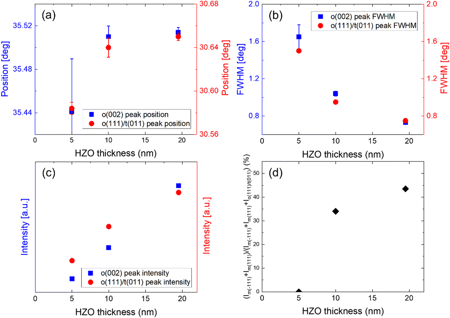 | ||
| Fig. 1 The (a) peak positions, (b) FWHM, and (c) peak intensities of the o(002) and o(111)/t(011) peaks, and the (d) m-phase areal ratio for the undoped 5, 10, and 19.5 nm HZO films. Error bars are included for the peak positions and FWHM values from the standard deviation of the Gaussian fitting. | ||
Fig. 1(b) shows the changes in the FWHM values of the deconvoluted o(002) and o(111)/t(011) peaks, respectively. The FWHM of both o(002) and o(111)/t(011) peaks showed a gradual decrease due to the grain size increase with the increasing thickness. Fig. 1(c) shows the changes in the peak intensities of the deconvoluted o(002) and o(111)/t(011) peaks, respectively. Both peaks showed a gradual intensity increase attributed to the enhanced grain growth with increasing HZO thickness.
Fig. 1(d) shows the relative m-phase fraction changes with increasing thickness. The m-phase GIXRD peak areal fraction was calculated using (Im(−111) + Im(111))/(Im(−111) + Im(111) + Io(111)/t(011)), where Ix(hkl) denotes the areal intensity of the x(hkl) peak in the GIXRD pattern.11,35 Previous studies indicated the desirable rapid thermal annealing (RTA) temperature for the crystallization of HZO films to enhance their FE properties and minimize the m-phase formation 450–500 °C.2,15,29,34 This study employed a slightly higher RTA annealing temperature of 525 °C to investigate the effect of the ILs on the m-phase formation (or suppression) more clearly in the subsequent sections. The 5 nm HZO did not exhibit any m-phase, whereas the 10 nm HZO and 19.5 nm HZO showed a significant m-phase areal fraction increase up to ∼34% and ∼44% due to the enhanced grain growth in the thicker films.2,28,29,34,35 The peak positions, FWHM, peak intensities, and m-phase areal fractions of the undoped HZO films observed in this section serve as a reference in the subsequent sections for the doped films.
2.2 Al2O3-inserted HZO film
Fig. S2(a) and (b) in the ESI,† show GIXRD patterns of the as-deposited Alp(10 nm) and Alp(19.5 nm) samples, respectively. The Al2O3 IL insertion did not significantly affect the amorphous-like structure of the Alp(10 nm) films. However, it slightly suppressed the as-deposited crystallization for the thicker Alp(19.5 nm) HZO films, indicating a potential reduction of the m-phase after PMA.35,44Fig. S3(a) and (b) in the ESI,† show the background subtracted GIXRD patterns and the Gaussian deconvoluted curves of the 5, 10 nm HZO, and Alp(10 nm) samples after PMA. Fig. 2(a) shows the changes in the 2θ positions of the deconvoluted o(002) and o(111)/t(011) peaks for the Alp(10 nm) samples with changing Al2O3 IL cycles, respectively, where p = 0 case corresponds to the 10 nm HZO film. In Fig. 2(a), the blue and red dashed lines indicate the positions of the 5 nm HZO film for the o(002) and o(111)/t(011) peaks, respectively. In both peak cases, the changes displayed differences for the Al1, 2(10 nm) and Al3, 4, 6, and 8(10 nm) samples. Both o(002) and o(111)/t(011) peak positions of the Al1, 2(10 nm) samples were shifted to higher 2θ positions compared to the 10 nm HZO. According to Seo et al., the shift of the peaks to a higher position at low Al2O3 ALD cycles was attributed to Al3+ ions (ionic radius: 53.5 pm) substitutionally diffusing into the Zr4+ sites (ionic radius: 72 pm) without interrupting the continuous growth, causing in-plane tensile stress to the film.39 Due to the similar radius of the Hf4+ ions (ionic radius: 72 pm) to the Zr4+ ions, a similar insertion trait is expected for the HZO films. In contrast, the positions of the Al3, 4, 6, and 8(10 nm) films show a value similar to the 10 nm HZO (2θ ∼ 35.52° for o(002) and ∼30.64° for o(111)/t(011)). According to Seo et al., higher ALD cycles of Al2O3 formed a continuous layer, physically dividing the ZrO2 into two separate parts without diffusing into the Zr4+ sites and did not impose doping-induced stress.39 Therefore, the similar peak positions suggested that the thicker Al2O3 divided the 10 nm HZO films into two ∼5 nm parts.
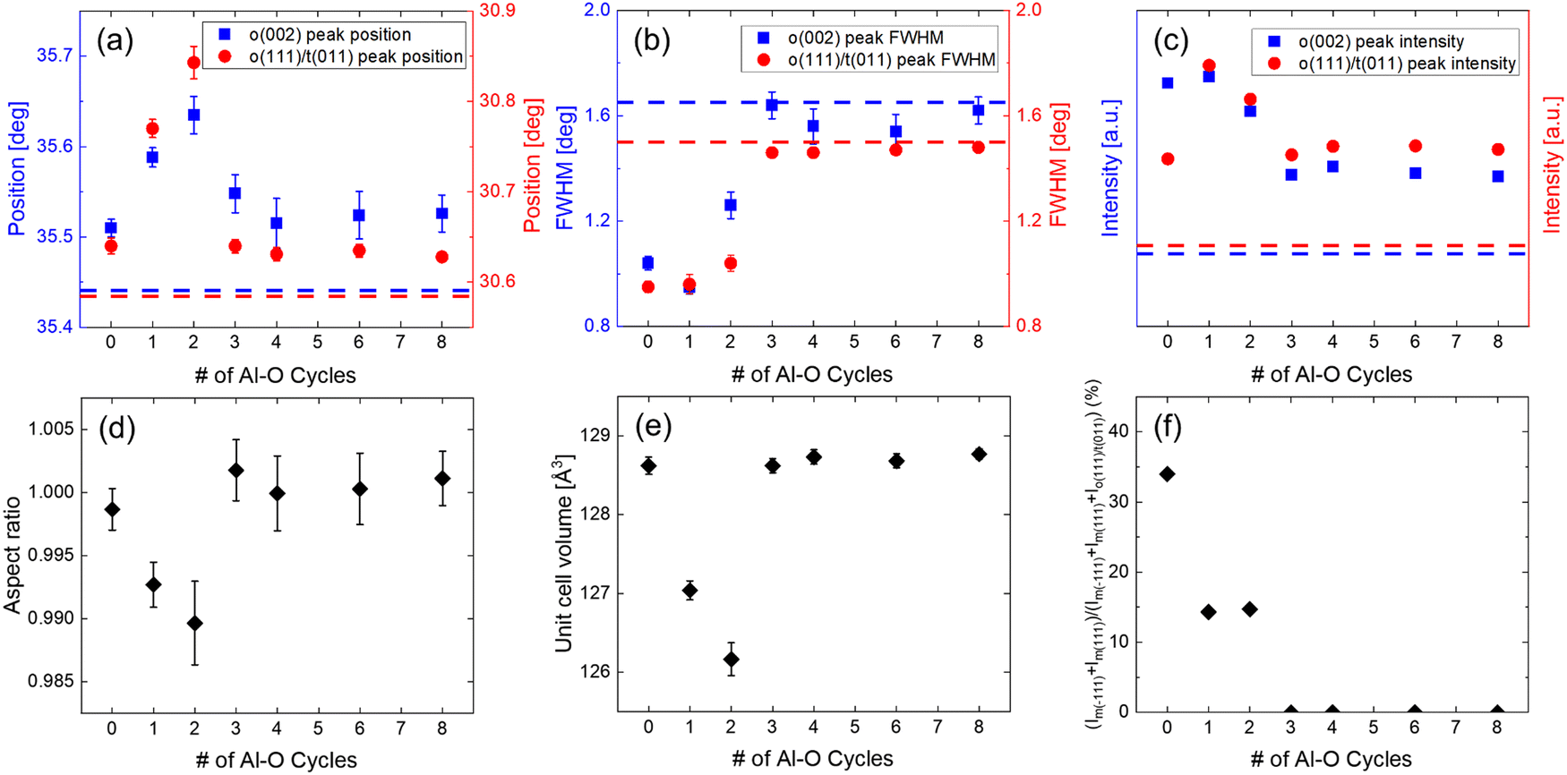 | ||
| Fig. 2 The (a) peak positions, (b) FWHM, and (c) peak intensities of the o(002) and o(111)/t(011) peaks, and the (d) aspect ratio, (e) unit cell volume, and (f) m-phase areal ratio for the Alp(10 nm) films. The 5 nm HZO is also added for comparison with blue (o(002) peak) and red (o(111)/t(011) peak) dashed lines. Error bars are included for the peak positions and FWHM values from the standard deviation of the Gaussian fitting. Error bars of the aspect ratio and unit cell volume are estimated from the error of the peak positions of the o(002) and o(111)/t(011) peaks. | ||
To confirm these Al2O3 IL insertion traits for the HZO films, spherical-aberration-corrected transmission electron microscopy (Cs-TEM) images of Al1(9 nm) and Al5(9 nm) after PMA are presented in Fig. 3(a) and (b), respectively. The Al1(9 nm) exhibited a well-crystallized single layer, suggesting that the extremely thin IL (∼0.1 nm) did not disrupt the continuous growth and diffused into the nearby HZO films. In contrast, the Al5 IL (∼0.5 nm) separated the HZO film into the upper and lower layers. These results were further supported by the inverse fast Fourier transform (iFFT) images in the inset figures, as well as the magnified images in Fig. 3(c) and (d). These TEM results corroborate the GIXRD results in Fig. 2(a). Therefore, the subsequent parts explain the Al1, 2(10 nm) and Al3, 4, 6, and 8(10 nm) samples separately.
 | ||
| Fig. 3 The Cs-TEM images of the (a) Al1(9 nm) and (b) Al5(9 nm) films, with the iFFT images of the regions indicated by the red squares. The magnified images of the regions indicated by the red squares are shown in (c) Al1(9 nm) and (d) Al5(9 nm), respectively. | ||
When comparing the position shifts of the Al1, 2(10 nm) samples in Fig. 2(a), it is noteworthy that the o(111)/t(011) peaks showed larger shifts compared to the o(002) peaks. Considering the minimal difference in inclination angles between the normal direction of the o(111)/t(011) and o(002) planes to the film surface normal direction, the εo(111)/t(011) strain induced by Al diffusion on the o(111)/t(011) planes should be similar to the εo(002) strain on the o(002) planes. Therefore, the observed differences in peak shifts should not be as pronounced as observed, suggesting factors other than in-plane tensile stress from Al diffusion may have additionally contributed to the observed o(111)/t(011) peak shifts. It can be assumed that the o(002) peaks were shifted by only the in-plane tensile stress from the diffused Al ions. In contrast, the o(111)/t(011) peaks may have been additionally shifted by an increased t(011)/(t(011) + o(111)) phase portion, as further discussed later.
When observing the peak positions of the Al3, 4, 6, and 8(10 nm) samples, it is noticeable that they have higher 2θ values than those of the 5 nm HZO, although the thicker ILs separate the 10 nm thick HZO film into two ∼5 nm HZO parts. As explained in the previous section, the bottom ∼5 nm HZO part must be influenced by the in-plane compressive stress from the nucleation.40–42 However, the top parts were grown on the amorphous Al2O3 layer, and consequently, the residual in-plane compressive stress could be released, shifting the peak positions to slightly higher 2θ values than the 5 nm HZO film. This shift must be more pronounced as the GIXRD is more sensitive to the top part of the film.
Fig. 2(b) shows the changes in the FWHM of the o(002) and o(111)/t(011) peaks for the Alp(10 nm) samples with changing Al2O3 IL cycles, respectively. The FWHM values of the Al1, 2(10 nm) for the o(002) (∼0.95–1.26) and o(111)/t(011) (∼0.96–1.04) peaks were similar to those of the 10 nm HZO (o(002): ∼1.04/o(111)/t(011): ∼0.95) since the interposed Al2O3 did not separate the HZO layer or disrupt the grain growth. In contrast, the FWHM values of the Al3, 4, 6, and 8(10 nm) for the o(002) (∼1.54–1.64) and o(111)/t(011) (∼1.46–1.48) peaks are similar to those of the 5 nm HZO (o(002): ∼1.65/o(111)/t(011): ∼1.50), also corroborating the layer separation effect of the thick Al2O3 layer.
Fig. 2(c) shows the changes in the peak intensities of the o(002) and o(111)/t(011) peaks for the Alp(10 nm) samples with changing Al2O3 IL cycles, respectively. The o(002) and o(111)/t(011) peak intensities of the Al3, 4, 6, and 8 (10 nm) were approximately twice that of the 5 nm HZO, confirming the presence of two separated ∼5 nm HZO layers. The o(002) peak intensities of the Al1, 2(10 nm) samples are comparable to those of the 10 nm HZO since the thin IL does not separate the 10 nm HZO film.
To confirm the speculations from peak positions shifts that the diffused Al enhanced the t(011)/(t(011) + o(111)) phase portion, the AR and unit cell volume changes were examined, as shown in Fig. 2(d) and (e), respectively. Park et al. suggested that the AR and unit cell volume are lower in the t-phase rich film than in the o-phase rich case for the polycrystalline HfO2-based thin films.13 It was extensively reported that the proportion of the o- and t-phases could be evaluated by observing the two factors.13,43 The AR and unit cell volume change could be calculated from the peak positions in Fig. 2(a). The lattice parameters were calculated from interplanar spacing d111 and d002 of o(111)/t(011) and o(002) peaks under the assumption that the differences of two shorter axis latter parameters were negligible. The AR (o-phase: 2a/(b + c), t-phase: c/a) and the unit cell volume (a × b × c) were calculated from the lattice parameters.13,43
For the Al1, 2(10 nm) samples, the AR and unit cell volume values were lower than the 10 nm HZO, indicating the enhanced portion of the t-phase relative to the o-phase. The decreased percentage of the AR values was ∼0.6–0.9%, smaller than the theoretical AR differences between the t- and o-phases (∼2%), indicating the co-existence of the o-phase in these films. However, the decreased percentage of the unit cell volume was ∼1.2–1.9%, comparable to the theoretical unit cell volume differences between the t- and o-phases (∼1.5–2%).43 This finding is because the Al-doping generally decreases the unit cell volume due to its smaller ionic radius than Hf4+ and Zr4+ ions.13 The AR and unit cell volume values of the Al3, 4, 6, and 8(10 nm) samples showed minimal changes since the division of the HZO films did not significantly affect the relative portion changes between the o- and t-phases as the diffused Al cases. The AR and unit cell volume changes correlated well with phase changes deduced from comparatively observing the o(002) and o(111)/t(011) peak shifts, confirming its validity.
Fig. 2(f) shows the relative m-phase fraction changes for the Alp(10 nm) samples with changing Al2O3 IL cycles. The Al3, 4, 6, and 8(10 nm) exhibited complete suppression of the m-phase due to the interrupted grain growth.2,28,29,34,35 This m-phase areal fraction was equal to the undoped 5 nm HZO, as the films were separated into two ∼5 nm-thick HZO layers.
The Al1, 2(10 nm) showed a markedly decreased m-phase areal fraction (∼15%) compared to the 10 nm HZO (∼34%), despite the Al2O3 not interrupting grain growth. The decreased m-phase must lead to the increase of the o- or t-phase portions in the films. Through a comparative analysis of the o(002) and o(111)/t(011) peak shifts, along with calculations of AR and unit cell volume of the Al1, 2(10 nm) films, it was concluded that there was an increased t/(o + t) phase portion with Al diffusion. Therefore, the dominant effect of Al diffusion appears to change the m-phase to the t-phase. The electrical characteristics tests were conducted to validate this hypothesis.
Fig. 4(a) shows the polarization–electric field (P–E) curves of the Alp(10 nm) samples in the pristine state (dotted curve for the 10 nm HZO for comparison). Fig. 4(b) shows the 2Pr and the +Ec − (−Ec) changes of the P–E curves displayed in Fig. 4(a). The 5 nm HZO film was too electrically leaky to achieve reliable P–E curves. The P–E data displayed distinct differences for the diffused Al2O3 and continuous Al2O3 samples, which is consistent with the GIXRD data. The Al1, 2(10 nm) samples showed antiferroelectric (AFE)-like P–E curves with lower 2Pr (∼22.8–24 μC cm−2) and +Ec − (−Ec) values (∼1.9–1.95 MV cm−1) compared to the 10 nm HZO, confirming that the Al diffusion decreased the m-phase and increased the t-phase. The curves did not show a complete AFE curve, as typically observed in the Zr-rich Hf1−xZrxO2 (0.7 ≤ x ≤ 1), due to the co-existence of the o-phase in these films.4,21,45 On the other hand, the Al3, 4, 6, and 8(10 nm) samples exhibited FE-like P–E curves with a slightly slanted shape. This behavior could be attributed to the marginal increase in the t/(o + t) phase portion caused by the reduced thickness of two separated ∼5 nm HZO layers, attributed to the lower surface energy of the t-phase than the o-phase.15,34,35 Nevertheless, the 2Pr values (∼34.7–36.5 μC cm−2) were higher than the Al1, 2(10 nm) samples, confirming a substantially more dominant o-phase portion in these films. These samples displayed higher +Ec − (−Ec) values (∼2.75–3.02 MV cm−1) than the 10 nm HZO, as the continuous Al2O3 layer acted as a series resistor during the FE switching.28,46 The gradual increase of the +Ec − (−Ec) values with increasing Al cycles (3–8 cycles) was attributed to the increasing tunneling resistance of the IL film with increasing its thickness.28,46
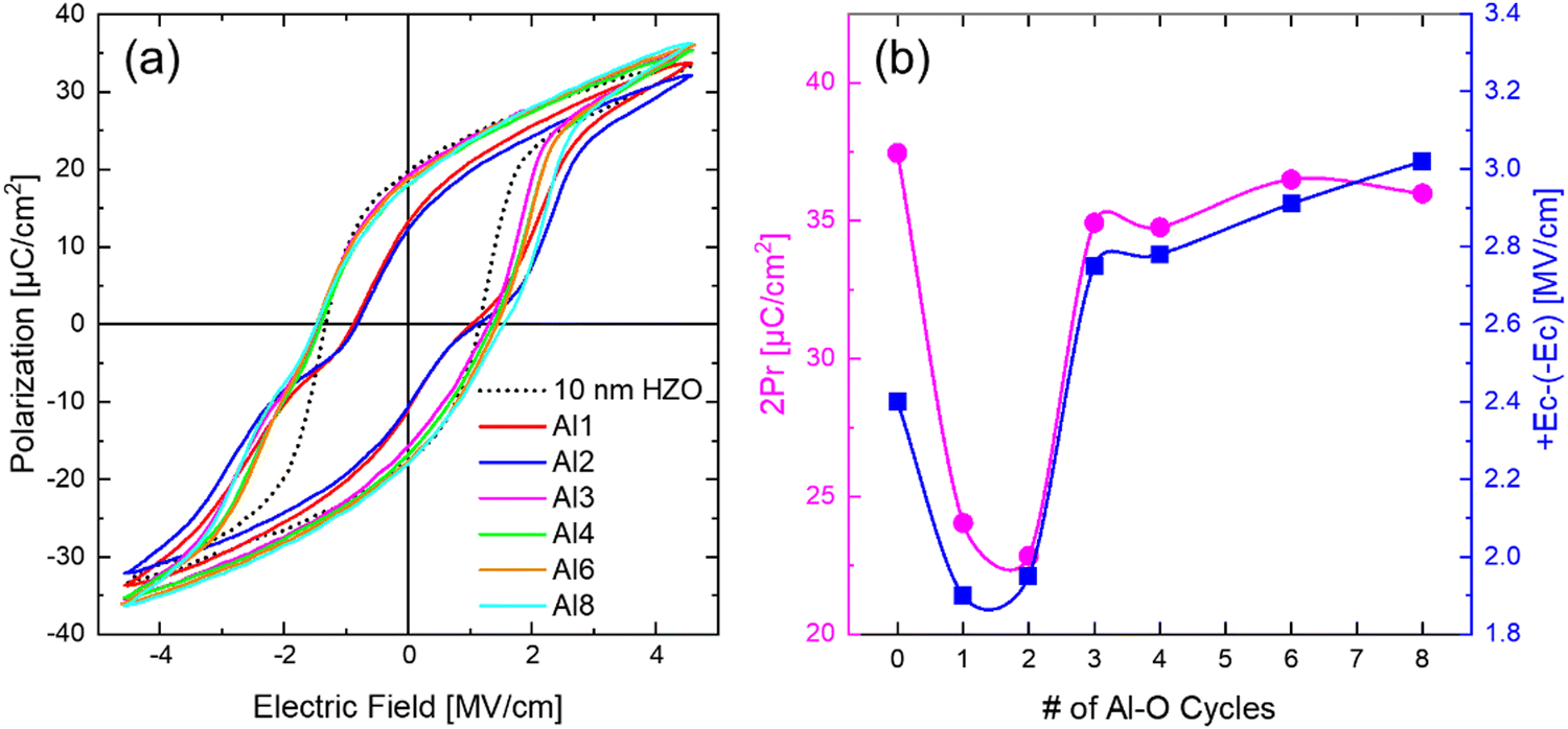 | ||
| Fig. 4 (a) P–E curves and the (b) changes in the 2Pr and +Ec − (−Ec) values of the 10 nm HZO with insertion of changing ALD cycles of Alp(10 nm) in the middle of films. | ||
Similar GIXRD and P–E analyses were performed for 10, 19.5 nm HZO, and Alp(19.5 nm) samples to validate these trends further. Fig. S4(a) and (b) in the ESI,† show the background subtracted GIXRD patterns and the Gaussian deconvoluted curves of the 10, 19.5 nm HZO, and Alp(19.5 nm) samples after PMA. Fig. S5(a)–(f) in the ESI,† show the peak position, FWHM, peak intensity, AR, unit cell volume, and m-phase areal ratio. The changes in these parameters for the Alp(19.5 nm) films indicated similar insertion effects and phase changes with the Alp(10 nm) samples. The thinner Al2O3 diffused into the nearby HZO, which reduced the m-phase and enhanced the t-phase. The thicker Al2O3 divided the HZO into two ∼10 nm parts.
However, there were several differences from the thinner film cases. For the Al3, 4, 6, and 8(10 nm) cases, both the o(002) and o(111)/t(011) peak positions showed noticeably higher shifts compared to those of the 5 nm HZO. However, the o(002) and o(111)/t(011) peak positions of the Al2, 3, 4, 6, and 8(19.5 nm) samples show negligible shifts compared to those of the 10 nm HZO. This difference is because the lower ∼10 nm HZO part of the Al2, 3, 4, 6, and 8(19.5 nm) samples were not influenced by the growth strain effects at this thickness, as explained in the previous section.
Also, Al2, 3, 4, 6, and 8(19.5 nm) samples showed retained m-phases with a peak areal fraction of ∼29–33%, in contrast to the Al3, 4, 6, and 8(10 nm) samples, where the m-phase was not observed. This difference was due to the thicker films being separated into two ∼10 nm-thick HZO layers, showing a similar m-phase areal fraction to the undoped 10 nm HZO (∼34%). Additionally, the AR and unit cell volume of Al1(19.5 nm), with the diffused Al2O3, decreased compared to the 19.5 nm HZO by ∼0.3% and ∼0.5%, showing smaller decreases compared to the Al1, 2(10 nm) cases in Fig. 2(d) and (e), indicating that the t-phase enhancement effects of the diffused Al2O3 for the Al1(19.5 nm) were less pronounced than the thinner Al1, 2(10 nm) films.
Fig. S6(a) and (b) in the ESI,† show the P–E curves and the changes in the 2Pr and +Ec − (−Ec) values of the Alp(19.5 nm) samples in the pristine state. The Al2, 3, 4, 6, and 8(19.5 nm) samples displayed increased 2Pr values due to the layer separation reducing the m-phase and enhancing the o/(m + o + t) phase portion in the films. The Al1(19.5 nm) sample with the diffused Al2O3 showed reduced 2Pr and +Ec − (−Ec) values compared to the undoped 19.5 nm HZO film, confirming that the diffused Al reduced the m-phase and enhanced the t-phase. However, the impact of diffused Al2O3 on the changes in electrical characteristics was less pronounced when inserted in the center of 19.5 nm HZO compared to 10 nm HZO. These results are consistent with AR and unit cell volume changes. It is plausible that the m-phase suppression and t-phase enhancement were more pronounced in the regions of the HZO film closer to the diffused Al2O3. The ratio of the HZO film affected by the t-phase enhancement may be smaller in the case of 19.5 nm HZO compared to 10 nm HZO, considering that the total thickness of HZO is approximately twice as large in the former case.
Fig. 5(a)–(c) show the X-ray photoelectron spectroscopy (XPS) spectra of Hf 4f, Zr 3d, and Al 2p, respectively, of the Al1, 3, and 5(7.8 nm) samples. The Hf 4f and Zr 3d spectra of the Al1(7.8 nm) sample shifted to lower binding energy positions than the 7.8 nm HZO. The deconvolution of these spectra revealed the formation of substantial oxygen-deficient phases (HfO2−x, ZrO2−x).25,47 These phases originated from the substitutional diffusion of Al3+ ions into the Hf4+ and Zr4+ ion sites, inducing oxygen vacancies to maintain charge neutrality.48 In contrast, the Hf 4f and Zr 3d spectra of Al3, 5(7.8 nm) samples showed minimal change in their binding energy values, and the deconvolution revealed the formation of minuscule oxygen-deficient phases. The Al 2p spectra in Fig. 5(c) showed that the binding energy of Al1(7.8 nm) (74.05 eV) was higher compared to those of Al3, 5(7.8 nm) (73.96 eV, 73.97 eV), suggesting that the Al oxidation number increased from the nominal 3+ in the Al2O3 for the diffused IL. These findings agree well with previous observations that the thick Al2O3 IL did not diffuse into the HZO but formed a separate layer. In contrast, the thin Al2O3 IL substitutionally diffused into the HZO. Previous studies indicated that creating a slightly oxygen-deficient condition for the HfO2-based films can suppress the m-phase formation and promote the t-phase.7,30,31,49,50 The diffused Al2O3 generated oxygen vacancies, effectively reducing the m-phase and enhancing the t-phase formation.
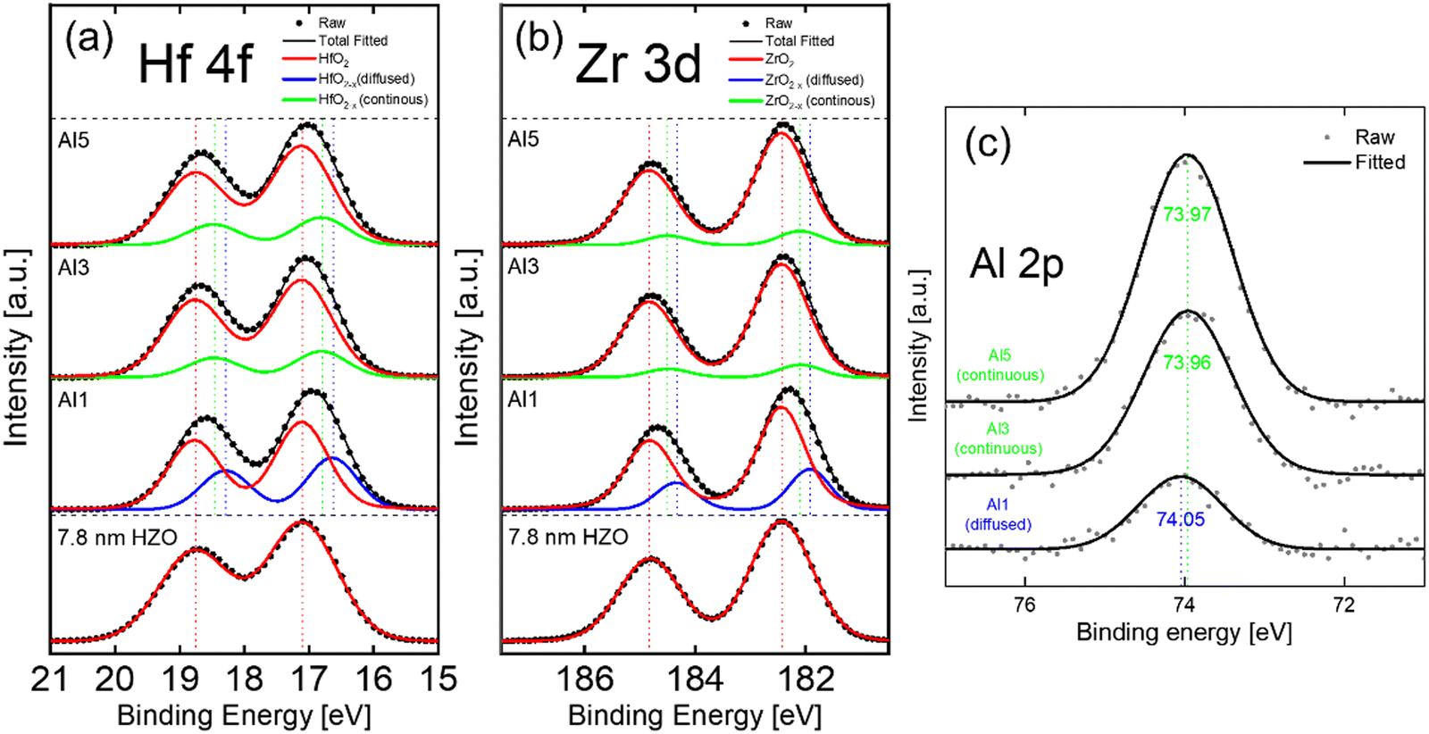 | ||
| Fig. 5 The baseline subtracted XPS (a) Hf 4f, (b) Zr 3d, and (c) Al 2p spectra of the Al1, 3, and 5(7.8 nm). The Hf 4f and Zr 3d spectra of the sample without interlayer are also compared. | ||
Fig. 6(a) and (b) summarize the effects of Al2O3 ILs when inserted in the middle of 10 nm and 19.5 nm HZO films. The thinner Al2O3 substitutionally diffused into the HZO without impeding the continuous growth and introduced in-plane tensile stress to the film. The Al2O3 layer reduced the m-phase and enhanced the t-phase due to the oxygen vacancies generated by the substitutional diffusion of Al3+ ions into the Hf4+ and Zr4+ sites in the 10 nm HZO film. The thicker HZO film was less influenced by the Al-doping effect, where only the region near the Al2O3 IL was affected.
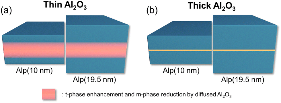 | ||
| Fig. 6 Schematic diagrams of the effects of Al2O3 ILs on the 10 nm and 19.5 nm HZO thin films. (a) The thin Al2O3 diffused into the HZO, inducing in-plane tensile stress. The diffusion enhanced the t-phase and reduced the m-phase for the nearby regions. The thicker 19.5 nm HZO film was less influenced by the diffusion. (b) The thick Al2O3 formed a continuous layer, dividing the film into two parts. | ||
In contrast, the thick Al2O3 layer remained a continuous layer. It separated the upper and lower regions of the HZO film, resulting in a significant reduction of the m-phase through suppressed grain growth. The formation of either the t-phase or the o-phase was favored depending on the physical thickness of the individual divided layers. Fig. S7(a)–(c) in the ESI,† shows the defect formation energy of the substitutional configurations of Al in the HZO. The calculation results coincide with the previous work, confirming the thickness-dependent substitutional diffusion characteristics of the Al2O3 ILs for the HZO system.39
2.3 Y2O3-inserted HZO film
Fig. S8(a) and (b) in the ESI,† show GIXRD of the as-deposited Yp(10 nm) and Yp(19.5 nm) samples, respectively. The Y2O3 IL insertion slightly enhanced the as-deposited crystallization of the HZO films, indicating a possible increase of the m-phase after PMA from conventional understanding.35,44 However, this study revealed a different trend, as discussed later.Fig. S9(a) and (b) in the ESI,† show the background subtracted GIXRD patterns and the Gaussian deconvoluted curves of the 10 nm HZO and Yp(10 nm) samples after PMA. Fig. 7(a) shows the changes in the 2θ positions of the deconvoluted o(002) and o(111)/t(011) peaks for the Yp(10 nm) samples with changing Y2O3 IL cycles, respectively. The o(002) peaks of Y1, 2, 4, 6, and 8(10 nm) were shifted monotonically to lower 2θ positions with increasing p. This peak position shift indicates the involvement of the in-plane compressive stress as the Y3+ ions (ionic radius: 90 pm) substitutionally diffuse into the Hf4+ and Zr4+ sites (ionic radius: 72 pm) without interrupting the continuous growth.39
 | ||
| Fig. 7 The (a) peak positions, (b) FWHM, and (c) peak intensities of the o(002) and o(111)/t(011) peaks, and the (d) aspect ratio, (e) unit cell volume, and (f) m-phase areal ratio for the Yp(10 nm) films. Error bars are included for the peak positions and FWHM values from the standard deviation of the Gaussian fitting. Error bars of the aspect ratio and unit cell volume are estimated from the error of the peak positions of the o(002) and o(111)/t(011) peaks. | ||
To check this Y2O3 IL insertion effect in HZO films, a Cs-TEM image of Y4(9 nm) after PMA is presented in Fig. 8(a), which exhibited a well-crystallized single layer. This observation was further supported by the iFFT image in the inset Fig and the magnified image in Fig. 8(b). Hence, these results suggested that the Y2O3 ILs substitutionally diffused into the nearby HZO films without interrupting the continuous growth.
 | ||
| Fig. 8 The (a) Cs-TEM image of the Y4(9 nm) film, with the iFFT image of the region indicated by the red square. The magnified image of the region indicated by the red square is shown in (b). | ||
In contrast, the o(111)/t(011) peak position shows a markedly different trend, as shown in Fig. 7(a). Up to two cycles of Y2O3 ALD, it increases and then decreases from four cycles, following the trend of the o(002) peaks. Following the discussion in the previous section, such a temporal increase in the peak position indicates the enhanced t(011)/(t(011) + o(111)) phase portion in the films. Again, such a trend cannot be detected from the o(002) peak, as only the strain evolution governs its position.
Fig. 7(b) shows the changes in the FWHM, and Fig. 7(c) shows the changes in the peak intensities of the deconvoluted o(002) and o(111)/t(011) peaks for the Yp(10 nm) samples with changing Y2O3 IL cycles, respectively. In the lower Y2O3 cycles, the FWHM of both o(002) and o(111)/t(011) peaks exhibited a gradual decrease compared to the 10 nm HZO film, while the peak intensities showed a gradual increase. These changes suggested that the diffused Y2O3 enhanced the grain growth at lower cycles. For higher Y2O3 cycles, the FWHM of both peaks showed increased values, accompanied by a decrease in peak intensities, suggesting that the HZO films developed into a mosaic structure.
To further confirm that the diffused Y enhanced the t/(o + t) phase portion, the AR and unit cell volume changes were presented in Fig. 7(d) and (e), respectively. The AR values of Yp(10 nm) samples decreased with increasing p at lower p, confirming that the Y diffusion enhanced the t/(o + t) phase portion.13,43 Interestingly, the AR values saturated at p ≥ 2. This saturation may be due to the limited impact of diffused Y2O3 on the phase changes within the nearby regions of the HZO, with regions farther away from the ILs remaining unaffected even with the increased p. The decreased percentage of the AR values was ∼0.5–1%, smaller than the theoretical AR differences between the t- and o-phases due to the copresence of the o-phase.43
The unit cell volume of Yp(10 nm) samples decreased up to p = 2 and increased for Y4, 6, and 8(10 nm). This change could be attributed to the combined influence of the relative portion changes between the o- and t-phases and the ionic radius of diffused Y3+.13 For p < 2, the t-phase formation effect dominates, but for p > 2, the larger Y3+ radius effect dominates.
Fig. 7(f) shows the relative m-phase fraction changes for the Yp(10 nm) samples with changing Y2O3 IL cycles. The Yp(10 nm) samples exhibited a remarkably decreased m-phase areal fraction of ∼5–13% compared to the 10 nm HZO (∼34%), despite the Y2O3 ILs not interrupting the continuous growth. This decrease indicated that the added portion of the o- and t-phases in the films increased compared to the undoped film. The observation of peak positions, AR, and unit cell volume of the Yp(10 nm) samples indicated the increased t/(o + t) phase portion with Y diffusion. Hence, the diffused Y2O3 reduces the m-phase and enhances the t-phase, as in the diffused Al2O3 cases. The following electrical characteristic tests confirmed this hypothesis.
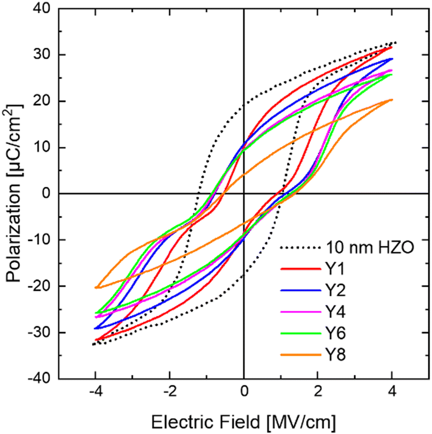
Fig. 9 shows the P–E curves of the Yp(10 nm) samples in the pristine state (dotted curve for the 10 nm HZO for comparison). They showed AFE-like P–E curves, confirming the m-phase reduction and the t-phase enhancement through Y diffusion. Similar to the Al1, 2(10 nm) cases, these films did not exhibit a complete AFE curve due to the copresence of the o-phase.4,21,45 The Y1, 2, 4, and 6(10 nm) samples exhibited similar 2Pr values (∼18.2–19.4 μC cm−2), indicating a comparable o-phase portion in these films. However, the Y8(10 nm) sample showed a degraded 2Pr value due to the formation of a mosaic structure and again increased m-phase fraction. The Y2, 4, and 6(10 nm) samples showed similar P–E curves despite the increased Y2O3 IL cycles. This result coincided with the AR values showing saturation at p ≥ 2 in Fig. 7(d), even with the increased p.
 | ||
| Fig. 9 P–E curves of the 10 nm HZO with insertion of changing ALD cycles of Yp(10 nm) in the middle of films. | ||
Similar GIXRD and P–E analyses were performed for 19.5 nm HZO and Yp(19.5 nm) samples to validate these trends further. Fig. S10(a) and (b) in the ESI,† show the background subtracted GIXRD patterns and the Gaussian deconvoluted curves of the 19.5 nm HZO and Yp(19.5 nm) samples after PMA. Fig. S11(a)–(f) in the ESI,† show the peak position, FWHM, peak intensity, AR, unit cell volume, and m-phase areal ratio. The changes in these parameters for the Yp(19.5 nm) films indicated similar insertion effects and phase changes with the Yp(10 nm) samples. However, while the Y doping exhibited consistent effects in thicker and thinner films, its impact was less prominent in the thicker Yp(19.5 nm) films.
Fig. S12 in the ESI,† shows the P–E curves of the Yp(19.5 nm) samples in the pristine state. The P–E curves exhibited reduced 2Pr values compared to the 19.5 nm HZO despite the significant m-phase reduction, confirming that the Y diffusion reduced the m-phase and enhanced the t-phase. However, its impact was less prominent than the thinner Yp(10 nm) cases, aligning with the GIXRD analysis.
Fig. 10(a)–(c) show the XPS spectra of Hf 4f, Zr 3d, and Y 3d, respectively, of the Y3, 5(7.8 nm) samples. The Hf 4f and Zr 3d spectra of the Y3, 5(7.8 nm) films shifted to lower binding energy positions than the 7.8 nm HZO, and deconvolution displayed the formation of oxygen-deficient phases (HfO2−x, ZrO2−x), coinciding with the Al1(7.8 nm) cases in Fig. 5(a) and (b).25,47 As for the diffused Al2O3 cases, the substitutional diffusion of Y3+ ions into the Hf4+ and Zr4+ ion sites generated oxygen vacancies, which reduced the m-phase and enhanced the t-phase.48 The Y 3d spectra in Fig. 10(c) showed minimal binding energy changes for Y3, 5(7.8 nm) samples since the ILs were substitutionally diffused regardless of cycles.
 | ||
| Fig. 10 The baseline subtracted XPS (a) Hf 4f, (b) Zr 3d, and (c) Y 3d spectra of the Y3, 5(7.8 nm). The Hf 4f and Zr 3d spectra of the sample without interlayer are also compared. | ||
Fig. 11 summarizes the effects of Y2O3 ILs when inserted in the middle of 10 nm and 19.5 nm HZO films. The Y2O3 IL, regardless of the number of cycles, substitutionally diffused into the HZO without hindering the continuous growth and induced stronger in-plane compressive stress to the HZO film with higher p. The diffused Y2O3 suppressed the m-phase and enhanced the t-phase formation due to the oxygen vacancies generated by the substitutional diffusion of Y3+ ions into the Hf4+ and Zr4+ sites. Fig. S7(a)–(c) in the ESI,† shows the defect formation energy of the substitutional configurations of Y in the HZO. The calculation results coincide with the previous work, thus confirming the thickness-independent substitutional diffusion characteristics of the Y2O3 ILs for the HZO system.39
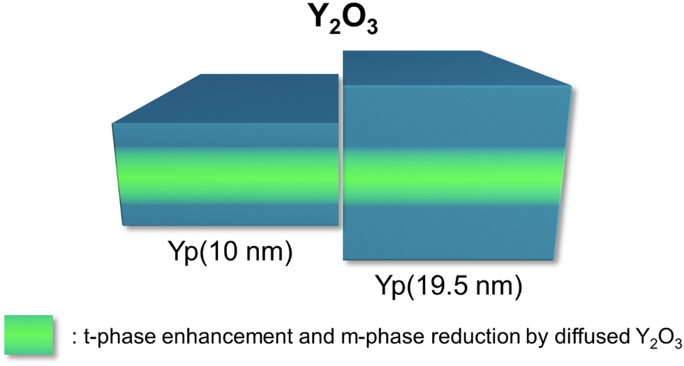 | ||
| Fig. 11 Schematic diagram of the effects of Y2O3 ILs on the 10 nm and 19.5 nm HZO thin films. The Y2O3 diffused into the HZO regardless of cycles, inducing in-plane compressive stress. The diffusion enhanced the t-phase and reduced the m-phase for the nearby regions. The thicker 19.5 nm HZO film was less influenced by the diffusion. | ||
Previous works have reported that dopants with ion sizes larger (Y, Gd, La, and Sr) and smaller (Si, Al) than Hf ions stabilize the c-phase and t-phase, respectively, for polycrystalline ALD HfO2-based films. When larger dopants were doped, the t-phase was not formed, and FFE characteristics were not observed. Only the smaller dopants could stabilize the t-phase and induce FFE properties.7
However, the present work revealed a different conclusion. It was revealed that the Y2O3 IL, irrespective of p, and the thin Al2O3 diffused into the HZO, reducing the m-phase and enhancing the t-phase. In contrast, the thick Al2O3 did not diffuse into the HZO and could not form the t-phase. Consequently, this study elucidated the substitutional diffusion of Al3+ or Y3+ ions into Hf4+ or Zr4+ sites and the formation of oxygen vacancies as the critical requirement factor determining the formation of the t-phase. Even larger Y dopants could stabilize the t-phase when the trivalent ions were substitutionally diffused. The t-phase stabilization was observed previously for epitaxial Y-doped HfO2/HZO films deposited by pulsed laser deposition (PLD). However, the t-phase stabilization was attributed to high annealing temperatures over 900 °C, converting the m-phase to the t-phase at such high temperatures, which was not the case in this study. In addition, these studies did not elucidate the substitutional diffusion of dopants as the reason for t-phase stabilization.51–53
These results suggest a new perspective on the phase changes of polycrystalline, doped-HfO2-based thin films, highlighting the crucial role of substitutional diffusion of dopants and charge neutrality. These insights could guide subsequent studies on engineering the FFE properties of doped HfO2-based thin films.
3. Experimental sections
3.1 Sample preparation
A TiN bottom electrode (BE) with a thickness of 50 nm was deposited on a thermally oxidized SiO2(100 nm)/Si substrate via sputtering (ENDURA 5500, Applied Materials). HZO films and Al2O3 ILs were deposited in situ by thermal ALD at a substrate temperature of 280 °C. Hf[N(C2H5)CH3]4 (TEMA-Hf), Zr[N(C2H5)CH3]4 (TEMA-Zr), Al(CH3)3 (TMA), and ozone (concentration: 190 g m−3) were used as the Hf, Zr, Al precursors, and oxygen source, respectively. Y2O3 ILs were deposited ex situ by the same thermal ALD at a substrate temperature of 250 °C. Y(EtCp)2(iPr-amd) (ARYA) and ozone (concentration: 260 g m−3) were used as the Y precursor and oxygen source, respectively. EtCp and iPr-amd represent ethylcyclopentadienyl (CH2CH3C5H5) and isopropylamidinate (CH(CH3)2CN2CH3), respectively. In all cases, the ILs were positioned in the middle of the HZO film thickness. The HfO2 and ZrO2 growth per cycle values were ∼0.14 nm per cycle, while those for Al2O3 and Y2O3 were ∼0.1 nm per cycle and ∼0.15 nm per cycle, respectively. The HZO films were deposited with different total numbers of HfO2 and ZrO2 ALD cycles, with most films being grown by 72 cycles (∼10 nm) or 140 cycles (∼19.5 nm). However, several films were prepared using 64 cycles (∼9 nm) or 56 cycles (∼7.8 nm). In all cases, the ALD cycle numbers for HfO2 and ZrO2 were the same to achieve a Hf:Zr composition ratio of 5:5.
3.2 Physical and electrical characterization
The physical thicknesses of each layer were determined using spectroscopic ellipsometry (SE; M-2000, J. A. Woollam), while the areal density (μg cm−2) and the cation composition were analyzed using X-ray fluorescence spectroscopy (XRF; Quant'X, Thermo SCIENTIFIC). Metal shadow masks (area: ∼90000 μm2) were used to deposit circular TiN (20 nm) top electrode (TE) via radio-frequency (RF) reactive sputtering (SRN 120, Sorona) at 500 W. The electrode areas were accurately measured with an optical microscope. After the TE deposition, PMA was performed at 525 °C for 30 s under an N2 ambient condition to crystallize the films.
The P–E characteristics were obtained by applying a bipolar triangular pulse at a frequency of 1 kHz with a ferroelectric tester (TF Analyzer 2000, Aixacct Systems). The 2Pr values were obtained by subtracting the negative y-intercept of the P–E curve from the positive y-intercept. The film crystal structure and crystallization behavior were analyzed via GIXRD (X'pert Pro, PANalytical, angle of incidence = 0.5°) and Cs-TEM (JEM-ARM200F, JEOL). XPS (Axis Supra, Kratos) analysis was performed to determine the chemical bonding state of Al2O3 and Y2O3 ILs with HZO films. The binding energy of the XPS spectra was calibrated using the adventitious C signal (284.5 eV).
4. Conclusions
In conclusion, this study systematically investigated the insertion mechanism of the Al2O3 and Y2O3 ILs and their effects on the structural and electrical properties of HZO film when inserted into the middle of films. It was revealed that the behavior of Al2O3 insertion varied depending on the number of Al2O3 IL cycles. The thin Al2O3 IL (1–2 cycles) diffused into the HZO films without interrupting continuous growth, which caused in-plane tensile stress to the films. In contrast, the thick Al2O3 IL (≥2–3 cycles) formed a continuous layer, physically dividing the HZO film into two discontinuous parts. The Y2O3 IL, regardless of the number of cycles, diffused into the HZO film, inducing in-plane compressive stress and enhancing grain growth. The most crucial finding of this work is that the substitutional diffusion of Al3+ and Y3+ ions into Hf4+ and Zr4+ ion sites generated oxygen vacancies for charge neutrality, forming oxygen-deficient phases near the diffused ILs, which reduced the monoclinic phase and enhanced the formation of the tetragonal phase. Unlike the previous understanding, the larger Y dopant could also induce the tetragonal phase when diffused into the HZO films. Hence, the substitutional diffusion of dopants was unveiled as the critical factor governing the tetragonal phase formation.The doping behavior of Al2O3 and Y2O3 ILs in the HZO system coincided with those reported by Seo et al. for the ZrO2 system.39 However, the two systems differed fundamentally because only the tetragonal phase was stabilized in the ZrO2 system. In contrast, the impurity type and quantity affected the phase changes in the HZO system. The changes in o- and t-phase portions were identified by comparatively observing the o(002) and o(111)/t(011) peak shifts and further confirmed by examining the AR and unit cell volume changes.
Author contributions
J. Shin designed and performed the experiments and wrote the manuscript. H. Seo assisted with the experiment design and data interpretations. K. H. Ye conducted the density functional theory calculations. Y. H. Jang helped with the figure design. D. S. Kwon, J. Lim, T. K. Kim, H. Paik, H. Song, S. J. Shin, and K. D. Kim helped review the manuscript. H. N. Kim, S. Y. Byun, Y. B. Lee, and I. S. Lee assisted with the ALD deposition and device fabrication. J.-H. Choi supervised the density functional theory calculations. C. S. Hwang supervised the whole research and manuscript preparation.Conflicts of interest
The authors declare they have no conflict of interest.Acknowledgements
This work was supported by the Next Generation Intelligence Semiconductor Foundation (No. 2022M3F3A2A01079620) and the Korea Evaluation Institute of Industrial Technology through the Technology Innovation Program (No. 20017216).Notes and references
- T. Böscke, J. Müller, D. Bräuhaus, U. Schröder and U. Böttger, Appl. Phys. Lett., 2011, 99, 102903 CrossRef.
- M. H. Park, Y. H. Lee, H. J. Kim, Y. J. Kim, T. Moon, K. D. Kim, J. Mueller, A. Kersch, U. Schroeder and T. Mikolajick, Adv. Mater., 2015, 27, 1811–1831 CrossRef CAS PubMed.
- M. H. Park, Y. H. Lee, T. Mikolajick, U. Schroeder and C. S. Hwang, MRS Commun., 2018, 8, 795–808 CrossRef CAS.
- M. H. Park and C. S. Hwang, Rep. Prog. Phys., 2019, 82, 124502 CrossRef CAS PubMed.
- U. Schroeder, C. S. Hwang and H. Funakubo, Ferroelectricity in doped hafnium oxide: materials, properties and devices, Woodhead Publishing, 2019 Search PubMed.
- M. H. Park, D. H. Lee, K. Yang, J.-Y. Park, G. T. Yu, H. W. Park, M. Materano, T. Mittmann, P. D. Lomenzo and T. Mikolajick, J. Mater. Chem. C, 2020, 8, 10526–10550 RSC.
- U. Schroeder, M. H. Park, T. Mikolajick and C. S. Hwang, Nat. Rev. Mater., 2022, 7, 653–669 CrossRef.
- S. Mueller, C. Adelmann, A. Singh, S. Van Elshocht, U. Schroeder and T. Mikolajick, ECS J. Solid State Sci. Technol., 2012, 1, N123 CrossRef CAS.
- S. Mueller, J. Mueller, A. Singh, S. Riedel, J. Sundqvist, U. Schroeder and T. Mikolajick, Adv. Funct. Mater., 2012, 22, 2412–2417 CrossRef CAS.
- J. Müller, T. Böscke, S. Müller, E. Yurchuk, P. Polakowski, J. Paul, D. Martin, T. Schenk, K. Khullar and A. Kersch, presented at 2013 IEEE International Electron Devices Meeting, 2013 Search PubMed.
- J. Muller, T. S. Boscke, U. Schroder, S. Mueller, D. Brauhaus, U. Bottger, L. Frey and T. Mikolajick, Nano Lett., 2012, 12, 4318–4323 CrossRef PubMed.
- J. Müller, U. Schröder, T. Böscke, I. Müller, U. Böttger, L. Wilde, J. Sundqvist, M. Lemberger, P. Kücher and T. Mikolajick, J. Appl. Phys., 2011, 110, 114113 CrossRef.
- M. H. Park, T. Schenk, C. M. Fancher, E. D. Grimley, C. Zhou, C. Richter, J. M. LeBeau, J. L. Jones, T. Mikolajick and U. Schroeder, J. Mater. Chem. C, 2017, 5, 4677–4690 RSC.
- T. Schenk, S. Mueller, U. Schroeder, R. Materlik, A. Kersch, M. Popovici, C. Adelmann, S. Van Elshocht and T. Mikolajick, presented at 2013 Proceedings of the European Solid-State Device Research Conference (ESSDERC), 2013 Search PubMed.
- M. H. Park, H. J. Kim, Y. J. Kim, W. Lee, T. Moon and C. S. Hwang, Appl. Phys. Lett., 2013, 102, 242905 CrossRef.
- M. H. Park, H. J. Kim, Y. J. Kim, W. Lee, T. Moon, K. D. Kim and C. S. Hwang, Appl. Phys. Lett., 2014, 105, 192903 CrossRef.
- M. H. Park, H. J. Kim, Y. J. Kim, T. Moon and C. S. Hwang, Appl. Phys. Lett., 2014, 104, 072901 CrossRef.
- T. Shimizu, T. Yokouchi, T. Shiraishi, T. Oikawa, P. S. R. Krishnan and H. Funakubo, Jpn. J. Appl. Phys., 2014, 53, 09PA04 CrossRef CAS.
- A. Chernikova, M. Kozodaev, A. Markeev, Y. Matveev, D. Negrov and O. Orlov, Microelectron. Eng., 2015, 147, 15–18 CrossRef CAS.
- R. Materlik, C. Künneth and A. Kersch, J. Appl. Phys., 2015, 117, 134109 CrossRef.
- M. H. Park, H. J. Kim, Y. J. Kim, Y. H. Lee, T. Moon, K. D. Kim, S. D. Hyun and C. S. Hwang, Appl. Phys. Lett., 2015, 107, 192907 CrossRef.
- M. H. Park, H. J. Kim, Y. J. Kim, T. Moon, K. D. Kim and C. S. Hwang, Adv. Energy Mater., 2014, 4, 1400610 CrossRef.
- M. H. Park, H. J. Kim, Y. J. Kim, Y. H. Lee, T. Moon, K. D. Kim, S. D. Hyun, F. P. G. Fengler, U. Schroeder and C. S. Hwang, ACS Appl. Mater. Interfaces, 2016, 8, 15466–15475 CrossRef CAS PubMed.
- B. Y. Kim, H. W. Park, S. D. Hyun, Y. B. Lee, S. H. Lee, M. Oh, S. K. Ryoo, I. S. Lee, S. Byun and D. Shim, Adv. Electron. Mater., 2022, 8, 2100042 CrossRef CAS.
- B. Y. Kim, I. S. Lee, H. W. Park, Y. B. Lee, S. H. Lee, M. Oh, S. K. Ryoo, S. R. Byun, K. D. Kim and J. H. Lee, Adv. Mater. Technol., 2023, 2300146 CrossRef CAS.
- D. Cunningham, Honors Scholar Thesis, 2014, 359 Search PubMed.
- S. Estandia, N. Dix, J. Gazquez, I. Fina, J. Lyu, M. F. Chisholm, J. Fontcuberta and F. Sanchez, ACS Appl. Electron. Mater., 2019, 1, 1449–1457 CrossRef CAS.
- H. J. Kim, M. H. Park, Y. J. Kim, Y. H. Lee, W. Jeon, T. Gwon, T. Moon, K. D. Kim and C. S. Hwang, Appl. Phys. Lett., 2014, 105, 192903 CrossRef.
- Y. H. Lee, S. D. Hyun, H. J. Kim, J. S. Kim, C. Yoo, T. Moon, K. D. Kim, H. W. Park, Y. B. Lee and B. S. Kim, Adv. Electron. Mater., 2019, 5, 1800436 CrossRef.
- T. Mittmann, T. Szyjka, H. Alex, M. C. Istrate, P. D. Lomenzo, L. Baumgarten, M. Müller, J. L. Jones, L. Pintilie and T. Mikolajick, Phys. Status Solidi RRL, 2021, 15, 2100012 CrossRef CAS.
- W. Hamouda, A. Pancotti, C. Lubin, L. Tortech, C. Richter, T. Mikolajick, U. Schroeder and N. Barrett, J. Appl. Phys., 2020, 127, 064105 CrossRef CAS.
- M. H. Park, H. J. Kim, G. Lee, J. Park, Y. H. Lee, Y. J. Kim, T. Moon, K. D. Kim, S. D. Hyun and H. W. Park, Appl. Phys. Rev., 2019, 6, 041403 Search PubMed.
- M. H. Park, Y. H. Lee and C. S. Hwang, Nanoscale, 2019, 11, 19477–19487 RSC.
- M. H. Park, Y. H. Lee, H. J. Kim, Y. J. Kim, T. Moon, K. Do Kim, S. D. Hyun, T. Mikolajick, U. Schroeder and C. S. Hwang, Nanoscale, 2018, 10, 716–725 RSC.
- M. H. Park, Y. H. Lee, H. J. Kim, T. Schenk, W. Lee, K. Do Kim, F. P. Fengler, T. Mikolajick, U. Schroeder and C. S. Hwang, Nanoscale, 2017, 9, 9973–9986 RSC.
- M. H. Park, Y. H. Lee, T. Mikolajick, U. Schroeder and C. S. Hwang, Adv. Electron. Mater., 2019, 5, 1800522 CrossRef.
- C.-K. Lee, E. Cho, H.-S. Lee, C. S. Hwang and S. Han, Phys. Rev. B: Condens. Matter Mater. Phys., 2008, 78, 012102 CrossRef.
- U. Schroeder, E. Yurchuk, J. Müller, D. Martin, T. Schenk, P. Polakowski, C. Adelmann, M. I. Popovici, S. V. Kalinin and T. Mikolajick, Jpn. J. Appl. Phys., 2014, 53, 08LE02 CrossRef CAS.
- H. Seo, I. W. Yeu, D. S. Kwon, D. G. Kim, J. Lim, T. K. Kim, H. Paik, J. H. Choi and C. S. Hwang, Adv. Electron. Mater., 2022, 8, 2200099 CrossRef CAS.
- Y. Lee, H. W. Jeong, S. H. Kim, K. Yang and M. H. Park, Mater. Sci. Semicond. Process., 2023, 160, 107411 CrossRef CAS.
- J. S. Tello and A. F. Bower, J. Mech. Phys. Solids, 2008, 56, 2727–2747 CrossRef.
- W. Nix and B. Clemens, J. Mater. Res., 1999, 14, 3467–3473 CrossRef CAS.
- M. H. Park, C. C. Chung, T. Schenk, C. Richter, K. Opsomer, C. Detavernier, C. Adelmann, J. L. Jones, T. Mikolajick and U. Schroeder, Adv. Electron. Mater., 2018, 4, 1800091 CrossRef.
- K. Do Kim, Y. H. Lee, T. Gwon, Y. J. Kim, H. J. Kim, T. Moon, S. D. Hyun, H. W. Park, M. H. Park and C. S. Hwang, Nano Energy, 2017, 39, 390–399 CrossRef.
- M. H. Park, H. J. Kim, Y. H. Lee, Y. J. Kim, T. Moon, K. Do Kim, S. D. Hyun and C. S. Hwang, Nanoscale, 2016, 8, 13898–13907 RSC.
- A. Q. Jiang, H. J. Lee, G. H. Kim and C. S. Hwang, Adv. Mater., 2009, 21, 2870–2875 CrossRef CAS.
- T. V. Perevalov, I. P. Prosvirin, E. A. Suprun, F. Mehmood, T. Mikolajick, U. Schroeder and V. A. Gritsenko, J. Sci.: Adv. Mater. Dev., 2021, 6, 595–600 CAS.
- M. Pešić, F. P. G. Fengler, L. Larcher, A. Padovani, T. Schenk, E. D. Grimley, X. Sang, J. M. LeBeau, S. Slesazeck and U. Schroeder, Adv. Funct. Mater., 2016, 26, 4601–4d612 CrossRef.
- M. Materano, P. D. Lomenzo, A. Kersch, M. H. Park, T. Mikolajick and U. Schroeder, Inorg. Chem. Front., 2021, 8, 2650–2672 RSC.
- Y. H. Lee, H. J. Kim, T. Moon, K. Do Kim, S. D. Hyun, H. W. Park, Y. B. Lee, M. H. Park and C. S. Hwang, Nanotechnology, 2017, 28, 305703 CrossRef PubMed.
- T. Mimura, T. Shimizu, T. Kiguchi, A. Akama, T. J. Konno, Y. Katsuya, O. Sakata and H. Funakubo, Jpn. J. Appl. Phys., 2019, 58, SBBB09 CrossRef CAS.
- T. Shimizu, Y. Tashiro, T. Mimura, T. Kiguchi, T. Shiraishi, T. J. Konno, O. Sakata and H. Funakubo, Phys. Status Solidi RRL, 2021, 15, 2000589 CrossRef CAS.
- T. Mimura, Y. Tashiro, T. Shimizu and H. Funakubo, ACS Appl. Electron. Mater., 2023, 5, 1600–1605 CrossRef CAS.
Footnote |
| † Electronic supplementary information (ESI) available. See DOI: https://doi.org/10.1039/d4tc00061g |
| This journal is © The Royal Society of Chemistry 2024 |