
 Open Access Article
 This Open Access Article is licensed under a
 Creative Commons Attribution 3.0 Unported Licence
A novel selenophene based non-fullerene acceptor for near-infrared organic photodetectors with ultra-low dark current †‡
Zhuoran
Qiao
 a,
Qiao
He
a,
Alberto D.
Scaccabarozzi
b,
Julianna
Panidi
a,
Adam
Marsh
c,
Yang
Han
d,
Polina
Jacoutot
a,
Davide
Nodari
a,
Tianyi
Zhang
a,
Amirah
Way
e,
Andrew J. P.
White
a,
Thomas D.
Anthopoulos
c,
Wing Chung
Tsoi
e,
Artem A.
Bakulin
a,
Martin
Heeney
*ac,
Zhuping
Fei
*f and
Nicola
Gasparini
*a
a,
Qiao
He
a,
Alberto D.
Scaccabarozzi
b,
Julianna
Panidi
a,
Adam
Marsh
c,
Yang
Han
d,
Polina
Jacoutot
a,
Davide
Nodari
a,
Tianyi
Zhang
a,
Amirah
Way
e,
Andrew J. P.
White
a,
Thomas D.
Anthopoulos
c,
Wing Chung
Tsoi
e,
Artem A.
Bakulin
a,
Martin
Heeney
*ac,
Zhuping
Fei
*f and
Nicola
Gasparini
*a
aDepartment of Chemistry and Centre for Processable Electronics, Imperial College London, London W12 0BZ, UK. E-mail: n.gasparini@imperial.ac.uk; m.heeney@imperial.ac.uk
bCenter for Nano Science and Technology, Politecnico di Milano, Istituto Italiano di Tecnologia, Raffaele Rubattino 81, Milano 20134, Italy
cKing Abdullah University of Science and Technology (KAUST), KAUST Solar Center (KSC), Thuwal 23955, Saudi Arabia
dSchool of Materials Science and Engineering and Tianjin Key Laboratory of Molecular Optoelectronic Science, Tianjin University, Tianjin 300350, China
eSPECIFIC, Faculty of Science and Engineering, Swansea University, Bay Campus, Fabian Way, Swansea SA1 8EN, UK
fInstitute of Molecular Plus, Tianjin Key Laboratory of Molecular Optoelectronic Science, Tianjin University, Tianjin 300072, China. E-mail: zfei@tju.edu.cn
First published on 22nd March 2024
Abstract
Near-infrared organic photodetectors (OPDs) have great potential in many applications. However, the high dark current of many OPD devices tends to limit their specific detectivity and overall performance. Here we report a novel non-fullerene acceptor (IDSe) based on an alkylated indacenodiselenophene core, with extended light absorption up to 800 nm. When blended with the donor polymer PTQ10, we obtained OPD devices with an exceptionally low dark current density of 1.65 nA cm−2 at −2 V, high responsivity and specific detectivity exceeding 1012 Jones at 790 nm. The superior properties of PTQ10:IDSe devices are related to the higher and more balanced charge carrier mobility compared to the analogous thiophene based blend (PTQ10:IDIC). We also demonstrate large area PTQ10:IDSe based devices by doctor blade in air with a record low dark current of 1.2 × 10⁻⁷ A cm−2 under −2 V bias.
 Nicola Gasparini | Dr Nicola Gasparini received his BSc and MSc, in Chemistry and Organic Chemistry, and Photochemistry and Molecular Materials, respectively, from the University of Bologna, Italy. In 2014 he joined the group of Professor Brabec in the Institute of Materials for Electronics and Energy Technology (i-MEET) at the Friedrich Alexander University Erlangen-Nürnberg (FAU) and received his PhD in 2017. In September 2017, he joined the King Abdullah University of Science and Technology (KAUST) as a postdoctoral fellow. In September 2019, he moved to the Department of Chemistry of Imperial College London as an independent researcher holding the Imperial College Research Fellowship. In early 2022, Nicola was appointed Lecturer in Chemistry (assistant professor, tenured) in the Department of Chemistry. His research interests are in organic and perovskite semiconductors, with particular interests in charge transport and recombination processes in solar cells and photodetectors. |
Introduction
Photodetectors (PDs) play a paramount role in sensing fields such as imaging, environmental monitoring, and machine vision to convert light into electrical signals.1 Despite the excellent device performance,2,3 commercial PDs feature high intrinsic brittleness and complicated manufacturing processes, which leads to high costs and limit the application in large-area flexible imagers. As a result, in the past few years, photodetectors based on organic materials have received increasing attention. Compared with inorganics, organic photodetectors (OPDs) use lightweight, flexible materials and offer potentially low fabrication costs, while having promising photogeneration yield.4–7 Moreover, by fine-tuning the optical bandgap of the organic material, OPDs can be engineered for high and specific light detection. In terms of the fabrication environment, OPDs can be processed from solution by employing different coating techniques ranging from spin coating, spray coating and doctor blading under ambient conditions.2 Depending on the wavelength of interest, organic photodetectors can be employed for ultraviolet, visible and near-infrared applications. The latter is useful for night-vision cameras, health monitoring and light communication technologies.6,8–11To maximize the light-to-current conversion, the active layer in OPD devices generally consists of a blend of electron-donating and electron-accepting organic semiconductor materials. The past few years have experienced the development of the so-called non-fullerene acceptors (NFAs), which overcome some of the intrinsic limitations of traditional fullerene and its derivatives, such as weak light absorption, limited energy-level tuning and blend instability. Small molecule NFAs show numerous attractive features, including high purity, crystallinity and lower reorganizational energy.12–16 Furthermore, the bandgap and energy levels can be readily tuned by varying the synthetic structure in order to achieve near-infrared light absorption.17–20
Numerous NFAs have been reported to date, with a popular design motif based on an electron-rich donor (D) core being flanked by two electron-deficient acceptor (A) units, the so-called A–D–A system. Analyzing the structures of reported NFAs, it is clear that many of the best performing contain thiophene-based fused aromatics within the donor core.21 This is likely due to a combination of factors, such as the well-developed chemistry of thiophene which facilitates their synthesis, as well as the diffuse orbitals of the sulfur heteroatom which may benefit intermolecular charge transport. An elegant strategy to shift the absorption windows >750 nm consists of replacing the thiophene moiety with selenophene. Selenophene has lower aromatic stabilization energy than thiophene, and the replacement of thiophene with selenophene in conjugated oligomers or polymers has been shown to increase the quinoidal character of the material, resulting in a reduced band gap and a red-shifted absorption.22–25 Furthermore, the larger, more polarisable Se atom can enhance the intermolecular interactions resulting in improved charge carrier mobility.26,27
Until now, few fused selenophene containing NFAs have been reported to date and to the best of our knowledge, all of those reported have contain aryl-based solubilizing groups at the bridgehead carbons.23,28–35 Although the aryl group affords good solubility to the NFA, we and others have recently demonstrated that the replacement of the alkylaryl groups with simple straight chain alkyl groups resulted in significant changes in the solid-state microstructure of thiophene-based NFAs and an overall enhancement in their power conversion efficiency (PCE) for organic solar cells.36–38 Encouraged by this observation, we report here the first preparation of a NFA containing a fused indacenodiselenophene with octyl sidechains at the bridgehead positions. This is the direct selenophene analogue of the previously indacenodithiophene acceptor known as IDIC, widely reported in the OPV community.39–41 We that note that IDIC typically uses hexyl sidechains, rather than octyl, but the octyl derivative has been reported with very similar properties to the hexyl derivative. In addition, analysis of the single crystal structures demonstrates similar packing of the conjugated cores for both sidechains.42,43
In this work, we show that the selenophene analogue exhibits a red-shifted absorption compared to the thiophene analogue, and when paired with a suitable wide band gap donor, organic photodetector devices using donor–acceptor bulk heterojunction configuration have an ultralow dark current density (Jd) of 1.65 nA cm−2 at −2 V and a specific detectivity (D*) of 1012 Jones at −2 V. In addition, higher and balanced carrier mobility is observed in the blend containing selenophene analogue compared to the thiophene benchmark. We also fabricated large-area OPDs (5 × 5 cm substrates) using doctor blade coating in air, a more scalable technique than spin-coating, and obtained low dark current density of 1.2 × 10⁻⁷ A cm−2 at −2 V.
Results and discussion
Synthesis and characterization
The synthesis of IDSe is shown in Scheme 1 and starts from our previously reported 2,7-bis(trimethylsilyl)-4,9-dihydro-s-indaceno[1,2-b:5,6-b′]bis(selenophene).44 Treatment with six equivalents of sodium tert-butoxide followed by 1-bromooctane resulted in a one-pot alkylation and desilyation, and subsequent bromination with NBS afforded compound 3 in a yield of 62% over the two steps. Treatment of 3 with n-BuLi in THF at −100 °C, followed by the addition of dry DMF afforded the dialdehyde 4 in 85% yield. We note that performing the lithiation at higher temperatures resulted in a considerable amount of decomposition, presumably by the ring opening of the selenophene following deprotonation at the alpha position. The final acceptor molecule IDSe was prepared by the Knoevenagel condensation reaction of 4 and 1,1-dicyanomethylene-3-indanone (IC) in 87% yield. | ||
| Scheme 1 Synthetic route to IDSe. | ||
The new acceptor showed good solubility in common organic solvents and was characterized by a combination of NMR and mass spectroscopy. A crystal of IDSe was successfully grown by slowly diffusing methanol into a solution of IDSe in dichloromethane at room temperature, and was analyzed by single-crystal X-ray diffraction, as shown in Fig. 1, with the crystallographic data are summarized in the (ESI†). The alkyl chains on the bridging carbons have been removed to aide visualization, but the full structure is shown in Fig. S1 (ESI†), with the octyl sidechains extending away from the backbone in a fully trans (or anti) conformation with two gauche defects. The IDSe shows a nearly planar conjugated backbone with a centre of symmetry at the middle of the benzene ring on IDSe unit, and a slight twist of 12.6° between the IDSe core and the IC endgroup, slightly smaller than the analogous IDIC (14.9°).45 Interestingly, the distance between Se and O atoms is around 2.71 Å, which is much shorter than their van der Waals radius (3.42 Å), indicating a non-covalent interaction which helps to lock the molecule in a single conformation. Analysis of the crystal packing (Fig. 1c and d) demonstrates that the molecules are arranged in a two-dimensional grid-like packing, with two parallel lines of molecules intersecting via the overlap of the IC endgoups. There is a strong overlap of the IC endgroups, with an interplanar distance of 3.46–3.50 Å, similar to IDIC. The voids in the structure shown in Fig. 1d are filled by residual solvent and the octyl sidechains. Such a packing arrangement forms an extended three dimensional packing arrangement that may be beneficial for exciton and charge transport. Analysis of spun-cast thin-films of both IDIC and IDSe by 2D GIWAXS (Fig. 1e and f) and scattering profiles (Fig. S11, ESI†) shows that both materials exhibit clear diffraction features along the vertical and horizontal directions. However, the IDSe appears more ordered than IDIC, both in terms of intensity and richness of the diffractions, for films of similar thickness.
 | ||
| Fig. 1 (a) Side and (b) front-view of IDSe crystal structure (alkyl sidechains removed for clarity) and the packing diagrams of IDSe project along the (c) b-axis and (d) c-axis showing close overlap of end-groups. 2D GIWAXS images of films of (e) IDIC and (f) IDSe. | ||
Thermogravimetric analysis indicated that IDSe has excellent thermal stability, with a decomposition temperature above 350 °C at 5% weight loss (Fig. S2, ESI†). Examination of the thermal behaviour by differential scanning calorimetry (DSC) demonstrated that IDSe exhibits two distinct melting peaks at 191 and 225 °C in the first heating cycle but forms a glass upon cooling (Fig. S3, ESI†). Upon subsequent heating, the glass undergoes two exothermic crystallization transitions at 130 and 156 °C, followed by a main endothermic melting transition at 210 °C in the second heating cycle. This behaviour is repeated in the third heating/cooling cycle.
IDSe exhibits an absorption maximum at 685 nm with a shoulder peak around 630 nm in dilute chlorobenzene solution with a high absorption coefficient (e) of 1.77 × 10⁵ M−1 cm−1 (Fig. S4, ESI†). In thin film, the absorption maximum is significantly red-shifted to 749 nm and the film absorbs strongly in the region from 600 to 800 nm, with an absorption edge at 800 nm corresponding to an optical band gap of 1.55 eV. In comparison to the reported thiophene analogue with hexyl sidechains (IDIC), changing to selenophene results in a red shift of 33 nm in the solid state and 21 nm in solution. The energy alignments of the IDSe in the solid state were evaluated via Photoelectron Spectroscopy in Air (PESA) measurements and cyclic voltammetry (PESA and CV, Fig. S5, ESI†) on a Pt working electrode. From the ionisation potential measured with PESA, the highest occupied molcule orbital (HOMO) energies of PTQ10, IDSe and IDIC were estimated as −5.20 eV, −5.79 eV and −5.81 eV, respectively. Whereas their lowest unoccupied molecular orbital (LUMO) were estimated adding the optical bandgap to the HOMO values. CV measurements allowed a direct measurement of the reduction (and oxidation) potentials, and demonstrated a similar trend to the PESA, albeit with different values. Thus, HOMO and LUMO levels of −5.70 eV and −3.92 eV were estimated for IDSe, and −5.74 eV and −3.90 eV for IDIC by reference to the ferrocene/ferrocenium couple with a HOMO of −4.8 eV. The HOMO is slightly upshifted compared to the thiophene analogue (IDIC), as is often observed in selenophene containing materials.22
Recently various NFA materials have demonstrated promising performance in thin-film transistor devices.46–49 Therefore we investigated the charge carrier behaviour of both acceptors in organic thin films transistors (OTFTs) fabricated in a bottom-contact, top-gate device architecture to evaluate holes and electrons mobility. For hole mobility measurements the source and drain electrodes were treated with a self-assembled monolayer in order to reduce the workfunction, whereas for electron mobility no surface treatments were performed.
Representative transfer and output characteristics of IDIC and IDSe OTFTs are presented in Fig. S6 and S7 (ESI†), where it can be seen that both materials show ambipolar behaviour, with IDSe having lower turn-on voltage and better overall performance. IDSe showed more than one order of magnitude higher charge carrier mobility than IDIC, with values of 0.16 and 0.22 cm2 V−1 s−1 for electrons and holes in the saturation regime, respectively, versus values of 0.002 and 0.009 cm2 V−1 s−1 for IDIC devices.
The higher charge carrier mobility of IDSe can be related to a combination of the more diffuse and polarizable Se orbitals,26,27 in combination with the more ordered packing and the overall higher crystallinity as observed from the GIWAXS measurements (Fig. 1).50
We fabricated organic photodetectors by blending IDSe with the p-type donor material PTQ10 for their complementary absorption and cascade energy alignment for efficient light-to-current conversion.51 The chemical structures of PTQ10 and the NFAs used and their absorption spectra are reported in Fig. 2a and b. Moreover, PTQ10 has been proven to be suitable for a thick active layer which is helpful to reduce dark current.52 The OPDs were fabricated in an inverted architecture consisting of ITO/ZnO/active layer/MoO3/Ag. Various fabrication parameters including solution concentration, donor–acceptor ratio, active layer thickness, thermal annealing temperature were carefully optimized. The current density–voltage (J–V) characteristics were measured both under light and in the dark conditions. Devices based on PTQ10:IDSe delivered ultra-low dark current density of 1.65 × 10⁻⁹ A cm−2 at −2 V, whereas PTQ10:IDIC showed a Jd of 4.67 × 10⁻⁸ A cm−2 at −2 V. The Jd values obtained in IDSe based OPDs are one of the lowest dark currents reported for NIR OPDs to the best of our knowledge.5
 | ||
| Fig. 2 (a) Chemical structures of PTQ10, IDIC and IDSe; (b) normalized absorbance of the neat materials; (c) energy levels of the materials extracted from PESA measurements; (d) schematic of the BHJ donor–acceptor device structure with inverted architecture. | ||
To fully understand the performance of OPDs further characterizations were conducted on both PTQ10:IDIC and PTQ10:IDSe devices. First, external quantum efficiency (EQE) was measured under different bias and converted into responsivity (R) using equation  . A 50 nm red-shift of responsivity is observed in PTQ10:IDSe devices, in agreement with the smaller band gap of IDSe, demonstrating the potential of selenophene based acceptors to promote near-infrared light detection.
To compare different PD devices, the most common figure of merit is the specific detectivity (D*), defined as  , where R is the responsivity, A is the device area, B is noise measurement bandwidth, and In Is the noise current.53 The noise spectrum was measured through a low noise amplifier and the results show that the PTQ10:IDSe device depicts a lower noise current spectral density level of 1 × 10⁻¹² A Hz−1/2 when compared to 3 × 10⁻¹² A Hz−1/2 of PTQ10:IDIC devices (Fig. 4a). The 1/f corner frequency,54 which is defined as the crossover point of 1/f noise and the broadband noise, also presents a different profile for two blends. The PTQ10:IDIC-based OPDs have a much higher frequency transition corner, indicating much higher flicker-noise dominating behaviour in the lower frequency area. The comparison of detectivity is plotted in Fig. 3c, indicating OPDs based on PTQ10:IDSe have a similar detectivity level in the visible light region and a higher detectivity into the NIR region, due to the extended absorption of IDSe.
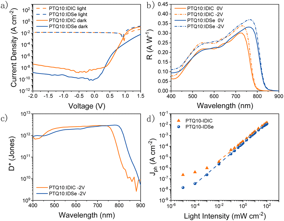 | ||
| Fig. 3 (a) Current density–voltage characteristics of PTQ10:IDIC and PTQ10:IDSe OPDs under dark and AM1.5G illumination; (b) responsivity and (c) specific detectivity of the OPD devices under negative bias applied; (d) linear dynamic range at −2 V for PTQ10:IDIC and PTQ10:IDSe under white light illumination. | ||
Photodetectors are expected to be operated at different light intensity depending on their application. For this reason we measured the J–Vs under different light conditions (Fig. S8, ESI†) and calculated the linear dynamic range (LDR).5,52,55 LDR is determined as the ratio between the maximum and the minimum photocurrent density (Jph![[thin space (1/6-em)]](https://www.rsc.org/images/entities/char_2009.gif) =Jl − Jd, where Jl and Jd refer to the current density at light and dark environment, respectively.) according to the equation
=Jl − Jd, where Jl and Jd refer to the current density at light and dark environment, respectively.) according to the equation  . Plotted in Fig. 3d, PTQ10:IDSe delivered a 120 dB LDR compared to 80 dB for PTQ10:IDIC devices at −2 V. This result can be attributed to the lower dark current and noise current of the IDSe blend, which are helpful to maintain the linear light response and outperform IDIC under low light conditions.
Apart from the detection range, operating speed is of great importance when assessing the performance of a NIR OPD.56,57 Frequency response, which measures the frequency at which the photocurrent value drops to −3 dB, is a key figure of merit.58 The overall operating frequency is either limited by the charge carrier transient time or by the RC property of the intrinsic circuits which gives rise to the equation f−2−3dB = f−2tr + f−2RC, where ftr is the carrier transient time-limited frequency and fRC is the RC time constant-limited frequency.59Fig. 4b depicts the −3 dB cutoff frequency of 60 kHz and 220 kHz for OPDs based on PTQ10:IDIC and PTQ10:IDSe blends, respectively. For modern video applications, 10 kHz is a benchmark for fast speed detection.56 Therefore, both blend combinations are competitive candidates for fast speed OPDs. To further understand the charge carrier transient characteristics, the rise and fall dynamics are investigated by illumination with a high-frequency continuous square-wave LED. Fig. 4c shows the rise and fall time of both devices. The rise time represents the time-interval for the signal to respond between 10% and 90% of the maximum value, and the vice versa for fall time.60 PTQ10:IDSe exhibited slightly faster transient time characteristics than PTQ10:IDIC devices, as summarized in Table 1. Rise and fall times are dependent on the mobility, recombination and extraction processes of charge carriers, which indicate faster mobility and efficient recombination processes might play significant roles.
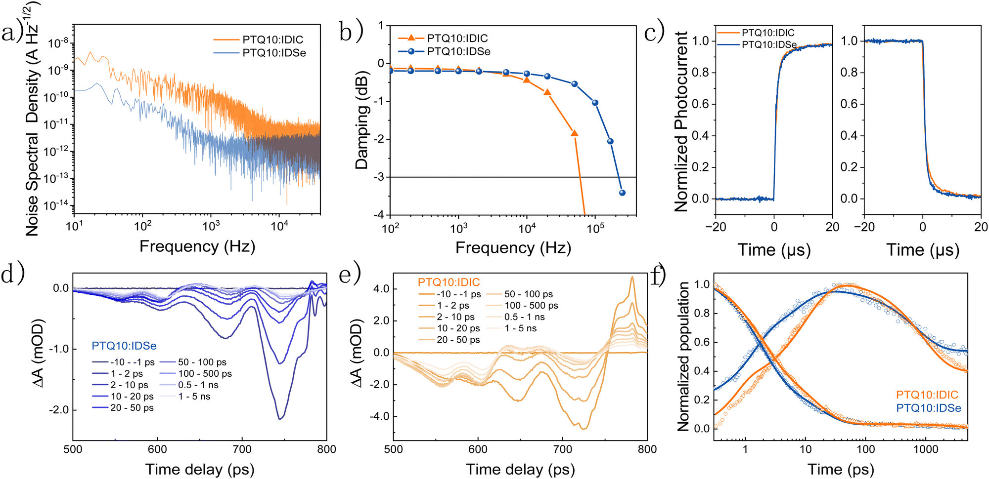 | ||
| Fig. 4 (a) Noise current spectral density, (b) cut-off frequency and (c) transient photocurrent measurements at −2 V for IDSe and IDIC-based OPD. Visible TA spectra for (d) PTQ10:IDSe blend and (e) PTQ10:IDIC blend films at different pump–probe delay times. Both samples were excited at 700 nm with a fluence of 2 μJ cm−2. (f) Deconvoluted kinetics of excitons (triangles) and charges (circles) in PTQ10:IDIC (orange) and PTQ10:IDSe (blue). Solid lines are monoexponential fittings of the decay and rise dynamics. | ||
| R (A W−1) | LDR (dB) | D* (Jones) | Rise time (μs) | Fall time (μs) | μ sclc(e) (cm2 V−1 s−1) | μ sclc(h) (cm2 V−1 s−1) | |
|---|---|---|---|---|---|---|---|
| PTQ10:IDIC | 0.35 (730 nm) | 80 | 2.86 × 10¹² | 3.6 | 7.0 | 2.1 × 10⁻⁵ | 1.6 × 10⁻⁵ |
| PTQ10:IDSe | 0.37 (770 nm) | 120 | 3.02 × 10¹² | 3.3 | 5.5 | 1.3 × 10⁻⁴ | 1.3 × 10⁻⁴ |
In order to explain the possible reason for the low dark current and excellent NIR performance of OPDs based on PTQ10:IDSe blend, charge carrier mobility was measured using the steady-state space-charge limited current (SCLC) method. Hole-only (glass/ITO/PEDOT:PSS/active layer/MoO3/Ag) and electron-only (glass/ITO/ZnO/active layer/DPO/Ag) devices were fabricated and measured. The J–V plot of single-carrier devices (Fig. S9, ESI†) was fitted using equation  where the ε represents the material relative dielectric constant (assumed to have a value of 3), ε0 indicates the vacuum permittivity and μ0 is the mobility at zero-field. Vbi is the built-in potential, L is the thickness of the active layer measured by the profilometer, γ is the field activation factor of mobility.61 For field-dependent diffusion, the result extracted from the previous equation was brought into the Poole–Frenkel expression which can be written as
  . The values of hole and electron mobility were calculated for a field of 5 × 10⁻⁴ V cm−1 corresponding to a potential of 0.5 V across a 100 nm thick film.
The pristine NFA materials depicted an electron mobility of 4.3 × 10⁻⁴ cm2 V−1 s−1 and 1.2 × 10⁻⁴ cm2 V−1 s−1 for IDSe and IDIC, respectively. The higher SCLC mobility calculated for IDSe is in line with that observed for the OTFT devices. As expected upon blending the NFAs with the donor polymer, the electron mobility for both acceptors drops, but to a lesser degree for IDSe. Thus electron and hole mobility for PTQ10:IDSe are equivalent at 1.3 × 10⁻⁴ cm2 V−1 s−1, respectively, whereas PTQ10:IDIC afforded electron and hole mobilities of 2.1 × 10⁻⁵ cm2 V−1 s−1 and 1.6 × 10⁻⁵ cm2 V−1 s−1. These results indicate that in the PTQ10:IDSe blend both hole and electron mobility are higher and more balanced (1.00 μh/μe ratio) than that in PTQ10:IDIC blend (0.76 μh/μe ratio). The balanced electron/hole mobility is effective for suppressing bimolecular recombination, which translates to lower dark current level.62
Examination of the blend morphology with GIWAXS demonstrates that both films exhibit similar microstructure (Fig. S10 and S11, ESI†), with clear diffraction peaks assignable to both the polymer and NFA crystallites. No obvious differences were apparent, suggesting that the higher charge mobility stemming from the replacement of thiophene with selenophene is the principal reason for the better OPD performance.
Next, we further examine the underlying exciton and charge dynamics in these two systems using ultrafast transient absorption spectroscopy. Fig. 4d and e compares the visible time-resolved spectra of the two OPD blends. In both blends, the acceptor was selectively excited with 700 nm pump at low fluence, thereby taking care to avoid exciton–exciton and exciton–charge annihilation events which dominate early recombination and dissociation dynamics. In the IDSe-based blend, the initial peak at 745 nm is assigned to the IDSe exciton. This initial peak is present in the neat IDSe TA spectra in Fig. S12b (ESI†) and is assigned to ground state absorption (GSB) of the acceptor. From the neat IDSe measurements, we extract an exciton lifetime of 26 ps, which is comparable with previously reported lifetimes of IDIC excitons.63
It is, however, apparent from the evolution of the blend spectra in time that other spectral components dominate at later times. Namely, we observe a slower decay of the GSB peaks at 560 and 604 nm in both blends, which we attribute to PTQ10 based on its neat TA data presented in Fig. S12a (ESI†). Furthermore, both blends demonstrate a clear growth of a positive photoinduced absorption (PIA) signal around 620–740 nm for IDSe blend and around 620–680 nm for the IDIC blend. Given the strong spectral overlap of the GSB and PIA features from D/A domains, we performed global analysis of the TA data for both blends. The results are deconvoluted spectra (Fig. S13, ESI†) of individual excited state species in the blend with their associated dynamics. The kinetic traces of the two spectral components are presented in Fig. 4f. Since we selectively excited the acceptor, we assign the decaying component to the IDSe and IDIC exciton (blue and orange triangles, respectively), while any later signal evolution is attributed to charge transfer states and free polaron formation. IDSe blend exhibits a 2 ps rise of the charge component, which subsequently decays within 710 ps. Analogous components in the IDIC blend resulted in 3 ps exciton decay accompanied by 3 ps charge generation, which then decayed within 820 ps. The PTQ10:IDIC excited state dynamics are in good agreement with a previously reported spectroscopic study.63 Overall, both blends exhibit fast exciton quenching and subsequent charge generation within 2–3 ps. While IDSe blend generates charges marginally faster, both blends exhibit efficient charge generation, which could be linked to high crystallinity of both blends, which tends to favour unbound charge transfer states over bound ones, which more readily generate free charges.64
Finally we tested PTQ10:IDSe devices under bias-stress in the dark to investigate their stability. The results indicates that PTQ10:IDSe devices have an excellent stability, maintaining the ultra-low dark current density of 6.30 nA cm−2 and LDR of 100 dB after 92 hours of continuous bias applied (Fig. S14 and S15 (ESI†), respectively). For real-world applications, spin coating is not feasible for large-area coating techniques. For this reason, we fabricated OPD devices on 5 × 5 cm ITO substrates by blade coating PTQ10:IDSe in air with an active area of 0.3 cm−2. The OPD devices delivered a dark current density of 1.2 × 10⁻⁷ A cm−2 under −2 V bias (Fig. 5a). Despite the higher Jd value compared to the small-area devices, which can be attributed to a non-homogenous coating of the active layer on large substrates and in air, this low value can be ranked among the top low dark current for large-area devices according to the reported literature.65,66 These results indicate the high potential of chalcogen engineering as a strategy to develop high performing blends for OPD devices.
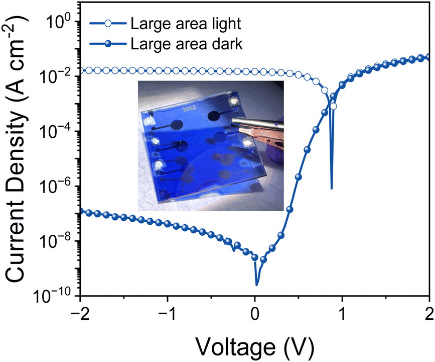 | ||
| Fig. 5 (a) Current–voltage characteristics of large-area PTQ10:IDSe-based devices under AM1.5G illumination and dark; in inset the picture of the large-area device (5 × 5 cm substrates). | ||
Conclusion
In conclusion, we report a new non-fullerene acceptor IDSe based on an indacenodiselenophene core functionalized with linear alkyl chains. This is the direct selenium analogue of the well known thiophene based acceptor IDIC, and to the best of our knowledge is the first indacenodiselenophene based NFA not containing aryl groups at the bridgehead positions. The replacement of sulfur with selenium results in a red-shift of the resulting acceptor, with an absorption extending 800 nm. X-ray analysis of IDSe single crystal shows an intermolecular non-covalent interaction between Se and O, and pronounced intramolecular interactions between the indanone endgroups. Thin film transistors of IDSe exhibit ambipolar behaviour, with balanced hole and electron transport that is over one order of magnitude higher than IDIC.Vis-NIR light-detecting organic photodetectors were fabricated with IDSe and its thiophene analogue IDIC from blends with the polymer donor PTQ10. OPDs based on the IDSe blend featured a Jd of 1.65 × 10⁻⁹ A cm−2 together with R of 0.37 A W−1 and D* of 3 × 10¹² Jones at 790 nm wavelength under −2 V bias. The ultralow Jd gives rise to an excellent 120 dB LDR under light illumination. While IDSe blend generates charges marginally faster than PTQ10:IDIC, their higher and balanced charge carried mobility values explain the lower dark current and superior optoelectronic performance. PTQ10:IDSe OPDs demonstrated outstanding stability under continuous −2 V bias in the absence of light. Finally we fabricated devices on 5 × 5 cm substrates by blade coating with an active area of 0.3 cm2, showcasing a record low Jd of 1.2 × 10⁻⁷ A cm−2 at −2 V bias, proving that PTQ10:IDSe blend has the ability to be applied in mass production in the future. These results demonstrate that alkylated indacenodiselenophene cores form promising building blocks for the fabrication of near-IR absorbing acceptors exhibiting high crystallinity.
Experimental
Synthesis and characterization
The synthetic route is outlined in Scheme 1 and described in further detail in the ESI.† Details of synthetic and characterization equipment and procedures can be found in the ESI.†Device fabrication
:1.5 ratio (wt/wt) in a 25 mg ml−1 concentration. The solutions were stirred overnight in the glove box at room temperature and heated to 40 °C 20 min before spin-coating to make sure materials were completely dissolved. The active layer solution was coated on the ZnO from the warm solution using a spin coater, under the nitrogen atmosphere, at different spin speeds ranging from 1000 rpm to 3000 rpm for 40 s. The active layers were then transferred onto a programmable heat plate in the glove box for 140 °C, 5 min thermal annealing (TA) treatment. For the thermal evaporation, a 10 nm MoO3 and a 100 nm Ag layer was sequentially deposited. The MoO3 layer was deposited at a 0.15 Å s−1 rate and in terms of Ag layer, deposition speed ranged from 0.5 Å s−1 to 1 Å s−1. Through a shadow mask, the area for each pixel is 0.045 cm2.
For the large-area devices, ITO-coated glass substrates (5 cm × 5 cm) were cleaned following the identical procedure as that of small-area devices. ZnO was uniformly deposited on the ITO by spin coating, forming a layer with 40 nm thickness. The active layer solution of PTQ10:IDSe was prepared using the same concentration and donor–acceptor ratio compared to the solution for small-area devices. The doctor blade coater (ZAA 2300 Automatic film applicator, Zehntner) was pre-heated to 40 °C by a temperature controller before fabrication. The gap between ZnO surface and the doctor blade was set to 400 μm while the coating speed ranged from 20 mm s−1 to 60 mm s−1. The substrates were continuously cleaned by the nitrogen gun until the start of coating. After doctor blade coating, 10 nm MoO3 and 100 nm Ag were thermally evaporated onto the active layer which was covered by a special mask. The J–V performance of large-area devices between −2 V to 2 V bias under light condition was measured under the standard AM1.5 solar simulator where both electrodes were linked to a Keithley 2400 source meter by alligator clips. Dark current was measured with aluminum foil covering the devices in order to create a completely dark environment.
Characterizations
Author contributions
Z. Q., Z. F., M. H and N. G. conceived and developed the ideas. Z. Q. designed the experiment, fabricated and characterised the OPD devices under the supervision of N. G. Q. H., Y. H, A. W. synthesised the materials under the superivsion of M. H., W. C. T. and Z. F. J. P., T. Z., and D. N. helped with the electrical characterisations. P. J. performed ultra-fast characterisations under the superivision of A. A. B. A. D. S. performed GIWAXS measurements under the supervision of T. D. A., A. J. P. W. performed XRD measurements. Z. Q., N. G. wrote the manuscript. All authors commented on the manuscript.Conflicts of interest
There are no conflicts to declare.Acknowledgements
The authors thank the Engineering and Physics Science Research Council (EPSRC) (EP/T028513/1 and EP/V057839/1), the King Abdullah University of Science and Technology (KAUST) Office of Sponsored Research (OSR) under Award No. OSR-2020-CRG8-4095 and ORFS-2023-OFP-5544, NSG Pilkington, the M2A funding from the European Social Fund through the Welsh Government. We are grateful to the SPECIFIC Innovation and Knowledge Centre (EP/N020863/1). A.D.S would like to thank the ALBA synchrotron (BL11 NCD-SWEET beamline) and staff, in particular Dr Eduardo Solano, for their help with the GIWAXS measurements.References
- P. C. Y. Chow and T. Someya, Adv. Mater., 2020, 32, 1902045 CrossRef CAS PubMed.
- C. Xie, X. T. Lu, X. W. Tong, Z. X. Zhang, F. X. Liang, L. Liang, L. B. Luo and Y. C. Wu, Adv. Funct. Mater., 2019, 29, 1806006 CrossRef.
- Y. Xu and Q. Lin, Appl. Phys. Rev., 2020, 7, 11315 CAS.
- Y. Z. Wang, J. Kublitski, S. Xing, F. Dollinger, D. Spoltore, J. Benduhn and K. Leo, Mater. Horiz., 2022, 9, 220–251 RSC.
- G. Simone, M. J. Dyson, S. C. J. Meskers, R. A. J. Janssen and G. H. Gelinck, Adv. Funct. Mater., 2019, 30, 1904205 CrossRef.
- F. P. García de Arquer, A. Armin, P. Meredith and E. H. Sargent, Nat. Rev. Mater., 2017, 2, 16100 CrossRef.
- T. Y. Zhang, M. Moser, A. D. Scaccabarozzi, H. Bristow, P. Jacoutot, A. Wadsworth, T. D. Anthopoulos, I. McCulloch and N. Gasparini, J. Phys. – Mater., 2021, 4, 045001 CrossRef CAS.
- X. Liu, Y. Lin, Y. Liao, J. Wu and Y. Zheng, J. Mater. Chem. C, 2018, 6, 3499–3513 RSC.
- Z. Wu, Y. Zhai, H. Kim, J. D. Azoulay and T. N. Ng, Acc. Chem. Res., 2018, 51, 3144–3153 CrossRef CAS PubMed.
- P. Jacoutot, A. D. Scaccabarozzi, T. Y. Zhang, Z. R. Qiao, F. Aniés, M. Neophytou, H. Bristow, R. Kumar, M. Moser, A. D. Nega, A. Schiza, A. Dimitrakopoulou-Strauss, V. G. Gregoriou, T. D. Anthopoulos, M. Heeney, I. McCulloch, A. A. Bakulin, C. L. Chochos and N. Gasparini, Small, 2022, 18, 2200580 CrossRef CAS PubMed.
- P. Jacoutot, A. D. Scaccabarozzi, D. Nodari, J. Panidi, Z. R. Qiao, A. Schiza, A. D. Nega, A. Dimitrakopoulou-Strauss, V. G. Gregoriou, M. Heeney, C. L. Chochos, A. A. Bakulin and N. Gasparini, Sci. Adv., 2023, 9, eadh2694 CrossRef CAS PubMed.
- J. Hou, O. Inganäs, R. H. Friend and F. Gao, Nat. Mater., 2018, 17, 119–128 CrossRef CAS PubMed.
- G. Y. Zhang, J. B. Zhao, P. C. Y. Chow, K. Jiang, J. Q. Zhang, Z. L. Zhu, J. Zhang, F. Huang and H. Yan, Chem. Rev., 2018, 118, 3447–3507 CrossRef CAS PubMed.
- C. Q. Yan, S. Barlow, Z. H. Wang, H. Yan, A. K. Y. Jen, S. R. Marder and X. W. Zhan, Nat. Rev. Mater., 2018, 3, 18003 CrossRef CAS.
- A. Armin, W. Li, O. J. Sandberg, Z. Xiao, L. M. Ding, J. Nelson, D. Neher, K. Vandewal, S. Shoaee, T. Wang, H. Ade, T. Heumüller, C. Brabec and P. Meredith, Adv. Energy Mater., 2021, 11, 2003570 CrossRef CAS.
- Q. He, P. Kafourou, X. T. Hu and M. Heeney, SN Appl. Sci., 2022, 4, 247 CrossRef CAS.
- A. Wadsworth, M. Moser, A. Marks, M. S. Little, N. Gasparini, C. J. Brabec, D. Baran and I. Mcculloch, Chem. Soc. Rev., 2019, 48, 1596–1625 RSC.
- H. W. Cheng, Y. P. Zhao and Y. Yang, Adv. Energy Mater., 2022, 12, 2102908 CrossRef CAS.
- W. Gao, F. R. Lin and A. K. Y. Jen, Sol. RRL, 2022, 6, 2100868 CrossRef CAS.
- X. T. Hu, Z. R. Qiao, D. Nodari, Q. He, J. Asatryan, M. Rimmele, Z. L. Chen, J. Martin, N. Gasparini and M. Heeney, Adv. Opt. Mater., 2023, 2302210 Search PubMed.
- J. Y. Wang and X. W. Zhan, Acc. Chem. Res., 2021, 54, 132–143 CrossRef CAS PubMed.
- A. V. Marsh and M. Heeney, Polym. J., 2023, 55, 375–385 CrossRef CAS.
- B. Fan, F. Lin, X. Wu, Z. Zhu and A. K.-Y. Jen, Acc. Chem. Res., 2021, 54, 3906–3916 CrossRef CAS PubMed.
- G. C. Hoover and D. S. Seferos, Chem. Sci., 2019, 10, 9182–9188 RSC.
- S. Y. Ye, V. Lotocki, H. Xu and D. S. Seferos, Chem. Soc. Rev., 2022, 51, 6442–6474 RSC.
- Y. H. Wijsboom, A. Patra, S. S. Zade, Y. Sheynin, M. Li, L. J. W. Shimon and M. Bendikov, Angew. Chem., Int. Ed., 2009, 48, 5443–5447 CrossRef CAS PubMed.
- M. Al-Hashimi, Y. Han, J. Smith, H. S. Bazzi, S. Y. A. Alqaradawi, S. E. Watkins, T. D. Anthopoulos and M. Heeney, Chem. Sci., 2016, 7, 1093–1099 RSC.
- H. Yu, Z. Y. Qi, J. Q. Zhang, Z. Wang, R. Sun, Y. Chang, H. L. Sun, W. T. Zhou, J. Min, H. Ade and H. Yan, J. Mater. Chem. A, 2020, 8, 23756–23765 RSC.
- H. Feng, X. L. Meng, L. Y. Fu, C. B. Liu, X. X. Yin, E. W. Zhu, Z. F. Li and G. B. Che, J. Mater. Chem. C, 2023, 11, 3020–3029 RSC.
- C. Yang, Q. S. An, H. R. Bai, H. F. Zhi, H. S. Ryu, A. Mahmood, X. Zhao, S. W. Zhang, H. Y. Woo and J. L. Wang, Angew. Chem., Int. Ed., 2021, 60, 19241–19252 CrossRef CAS PubMed.
- C. Labanti, M. J. Sung, J. Luke, S. Kwon, R. Kumar, J. S. Hong, J. Kim, A. A. Bakulin, S. K. Kwon, Y. H. Kim and J. S. Kim, ACS Nano, 2021, 15, 7700–7712 CrossRef CAS PubMed.
- X. Liu, X. Jiang, K. F. Wang, C. Y. Miao and S. M. Zhang, Materials, 2022, 15, 23 Search PubMed.
- J.-L. Wang, K.-K. Liu, L. Hong, G.-Y. Ge, C. Zhang and J. Hou, ACS Energy Lett., 2018, 3, 2967–2976 CrossRef CAS.
- Z. Liang, M. Li, X. Zhang, Q. Wang, Y. Jiang, H. Tian and Y. Geng, J. Mater. Chem. A, 2018, 6, 8059–8067 RSC.
- Y. Li, L. Zhong, F.-P. Wu, Y. Yuan, H.-J. Bin, Z.-Q. Jiang, Z. Zhang, Z.-G. Zhang, Y. Li and L.-S. Liao, Energy Environ. Sci., 2016, 9, 3429–3435 RSC.
- Q. He, M. Shahid, X. Jiao, E. Gann, F. D. Eisner, T. Wu, Z. Fei, T. D. Anthopoulos, C. R. McNeill and M. Heeney, ACS Appl. Mater. Interfaces, 2020, 12, 9555–9562 CrossRef CAS PubMed.
- Z. H. Luo, T. L. Xu, C. E. Zhang and C. L. Yang, Energy Environ. Sci., 2023, 16, 2732–2758 RSC.
- Z. Fei, F. Eisner, X. Jiao, M. Azzouzi, J. Röhr, Y. Han, M. Shahid, A. Chesman, C. Easton, C. McNeill, T. Anthopoulos, J. Nelson and M. Heeney, Adv. Mater., 2018, 30, 1705209 CrossRef PubMed.
- Y. Lin, Q. He, F. Zhao, L. Huo, J. Mai, X. Lu, C.-J. Su, T. Li, J. Wang, J. Zhu, Y. Sun, C. Wang and X. Zhan, J. Am. Chem. Soc., 2016, 138, 2973–2976 CrossRef CAS PubMed.
- Y. Li, N. Zheng, L. Yu, S. Wen, C. Gao, M. Sun and R. Yang, Adv. Mater., 2019, 31, 1807832 CrossRef PubMed.
- Y. Lin, F. Zhao, S. K. K. Prasad, J. D. Chen, W. Cai, Q. Zhang, K. Chen, Y. Wu, W. Ma, F. Gao, J. X. Tang, C. Wang, W. You, J. M. Hodgkiss and X. Zhan, Adv. Mater., 2018, 30, 1706363 CrossRef PubMed.
- Y. Zhang, Z. X. Liu, T. Shan, Y. Wang, L. Zhu, T. Li, F. Liu and H. L. Zhong, Mater. Chem. Front., 2020, 4, 2462–2471 RSC.
- X. J. Li, H. Huang, I. Angunawela, J. D. Zhou, J. Q. Du, A. Liebman-Pelaez, C. H. Zhu, Z. J. Zhang, L. Meng, Z. Q. Xie, H. Ade and Y. F. Li, Adv. Funct. Mater., 2020, 30, 1906855 CrossRef CAS.
- Z. Fei, Y. Han, E. Gann, T. Hodsden, A. S. R. Chesman, C. R. Mcneill, T. D. Anthopoulos and M. Heeney, J. Am. Chem. Soc., 2017, 139, 8552–8561 CrossRef CAS PubMed.
- J. F. Qu, H. Chen, J. D. Zhou, H. J. Lai, T. Liu, P. J. Chao, D. N. Li, Z. Q. Xie, F. He and Y. G. Ma, ACS Appl. Mater. Interfaces, 2018, 10, 39992–40000 CrossRef CAS PubMed.
- M. I. Nugraha, R. E. A. Ardhi, D. Naphade, W. M. Zhang, Y. Y. Yuan, M. Heeney and T. D. Anthopoulos, J. Mater. Chem. C, 2023, 11, 12941–12948 RSC.
- A. F. Paterson, R. P. Li, A. Markina, L. Tsetseris, S. MacPhee, H. Faber, A. H. Emwas, J. Panidi, H. Bristow, A. Wadsworth, D. Baran, D. Andrienko, M. Heeney, I. McCulloch and T. D. Anthopoulos, J. Mater. Chem. C, 2021, 9, 4486–4495 RSC.
- H. Bristow, K. J. Thorley, A. J. P. White, A. Wadsworth, M. Babics, Z. Hamid, W. M. Zhang, A. F. Paterson, J. Kosco, J. Panidi, T. D. Anthopoulos and I. McCulloch, Adv. Electron. Mater., 2019, 5, 1900344 CrossRef CAS.
- E. Gutierrez-Fernandez, A. D. Scaccabarozzi, A. Basu, E. Solano, T. D. Anthopoulos and J. Martín, Adv. Sci., 2022, 9, 2104977 CrossRef CAS PubMed.
- H. Tang, C. Yan, S. Karuthedath, H. Yin, Y. Gao, J. Gao, L. Zhang, J. Huang, S. So, Z. Kan, F. Laquai, G. Li and S. Lu, Sol. RRL, 2020, 4, 2300267 Search PubMed.
- C. Sun, F. Pan, H. Bin, J. Zhang, L. Xue, B. Qiu, Z. Wei, Z.-G. Zhang and Y. Li, Nat. Commun., 2018, 9, 743 CrossRef PubMed.
- H. Bristow, P. Jacoutot, A. D. Scaccabarozzi, M. Babics, M. Moser, A. Wadsworth, T. D. Anthopoulos, A. Bakulin, I. Mcculloch and N. Gasparini, ACS Appl. Mater. Interfaces, 2020, 12, 48836–48844 CrossRef CAS PubMed.
- F. Furlan, D. Nodari, E. Palladino, E. Angela, L. Mohan, J. Briscoe, M. J. Fuchter, T. J. Macdonald, G. Grancini, M. A. McLachlan and N. Gasparini, Adv. Opt. Mater., 2022, 10, 2201816 CrossRef CAS.
- F. N. Hooge, IEEE Trans. Electron Devices, 1994, 41, 1926–1935 CrossRef CAS.
- P. E. Keivanidis, P. K. H. Ho, R. H. Friend and N. C. Greenham, Adv. Funct. Mater., 2010, 20, 3895–3903 CrossRef CAS.
- R. D. Jansen-van Vuuren, A. Armin, A. K. Pandey, P. L. Burn and P. Meredith, Adv. Mater., 2016, 28, 4766–4802 CrossRef CAS PubMed.
- N. Strobel, N. Droseros, W. Köntges, M. Seiberlich, M. Pietsch, S. Schlisske, F. Lindheimer, R. R. Schröder, U. Lemmer, M. Pfannmöller, N. Banerji and G. Hernandez-Sosa, Adv. Mater., 2020, 32, 1908258 CrossRef CAS PubMed.
- J. Huang, J. Lee, J. Vollbrecht, V. V. Brus, A. L. Dixon, D. X. Cao, Z. Zhu, Z. Du, H. Wang, K. Cho, G. C. Bazan and T. Q. Nguyen, Adv. Mater., 2020, 32, 1906027 CrossRef CAS PubMed.
- M. Babics, H. Bristow, W. Zhang, A. Wadsworth, M. Neophytou, N. Gasparini and I. Mcculloch, J. Mater. Chem. C, 2021, 9, 2375–2380 RSC.
- M. Kielar, O. Dhez, G. Pecastaings, A. Curutchet and L. Hirsch, Sci. Rep., 2016, 6, 39201 CrossRef CAS PubMed.
- P. N. Murgatroyd, Journal of physics. D, Appl. Phys., 1970, 3, 151–156 CrossRef.
- G. Lakhwani, A. Rao and R. H. Friend, Annu. Rev. Phys. Chem., 2014, 65, 557–581 CrossRef CAS PubMed.
- H. Cha, Y. Zheng, Y. Dong, H. H. Lee, J. Wu, H. Bristow, J. Zhang, H. K. H. Lee, W. C. Tsoi, A. A. Bakulin, I. Mcculloch and J. R. Durrant, Adv. Energy Mater., 2020, 10, 2001149 CrossRef CAS.
- Y. Tamai, Y. Fan, V. Kim, K. Ziabrev, A. Rao, S. Barlow, S. Marder, R. Friend and S. Menke, ACS Nano, 2017, 11, 12473–12481 CrossRef CAS PubMed.
- C. Fuentes-Hernandez, W. Chou, T. Khan, L. Diniz, J. Lukens, F. Larrain, V. Rodriguez-Toro and B. Kippelen, Science, 2020, 370, 698 CrossRef CAS PubMed.
- Y. Lau, Z. Lan, L. Cai and F. Zhu, Mater. Today Energy, 2021, 21, 100708 CrossRef CAS.
- S. Gélinas, Doctor of Philosophy (PhD), University of Cambridge, 2013.
Footnotes |
| † Electronic supplementary information (ESI) available. See DOI: https://doi.org/10.1039/d3tc04678h |
| ‡ Amirah way could not be contacted to confirm the final author list prior to acceptance. |
| This journal is © The Royal Society of Chemistry 2024 |