
 Open Access Article
 This Open Access Article is licensed under a
 Creative Commons Attribution 3.0 Unported Licence
Reactive spin coating based on real-time in situ feedback for improved control of perovskite thin film fabrication†
Simon
Biberger
 a,
Maximilian
Spies
a,
Konstantin
Schötz
a,
Frank-Julian
Kahle
a,
Nico
Leupold
b,
Ralf
Moos
b,
Helen
Grüninger
c,
Anna
Köhler
a and
Fabian
Panzer
*a
a,
Maximilian
Spies
a,
Konstantin
Schötz
a,
Frank-Julian
Kahle
a,
Nico
Leupold
b,
Ralf
Moos
b,
Helen
Grüninger
c,
Anna
Köhler
a and
Fabian
Panzer
*a
aSoft Matter Optoelectronics (EP II), University of Bayreuth, Bayreuth 95440, Germany. E-mail: fabian.panzer@uni-bayreuth.de
bDepartment of Functional Materials, University of Bayreuth, Bayreuth 95440, Germany
cNorthern Bavarian NMR Centre (NBNC) and Inorganic Chemistry, University of Bayreuth, Bayreuth 95440, Germany
First published on 4th April 2024
Abstract
Efficient perovskite solar cells require metal halide perovskite (MHP) films of consistent and reproducible high quality. MHP films are frequently prepared through a solution-based solvent-engineering spin coating approach. This processing involves considering various controllable parameters (e.g. spin speed) and ones that are more difficult to control (e.g. changes in atmosphere) to fabricate MHP films reliably. To address this issue, we developed a closed-loop feedback system based on a multimodal optical in situ spectroscopy spin coater system. We combine this system with real-time monitoring and analysis of the optical spectra during the spin coating process. As soon as a parameter of interest reaches a predefined target level, perovskite crystallization is automatically induced by dispensing the antisolvent via a syringe pump. To demonstrate our approach, we optically monitor the precursor solution film thickness as the parameter of interest during the spin coating. We intentionally vary the evaporation kinetics by spin coating at different spin speeds between 2000 and 1250 rpm and compare our reactive method to the common time-based approach. We find that our method reliably counteracts effects like variation in solvent evaporation rate due to atmospheric changes and reduces the human impact on the processing, thus leading to reproducible film quality for all spin speeds without any optimization steps.
1. Introduction
With PCEs up to 26.1%1 and operational stabilities of several thousand hours,2,3 metal halide perovskites (MHP) based solar cells have improved tremendously in the last 10 years. These highly efficient solar cells require a high quality of the MHP film itself. The state-of-the-art processing method for the majority of such high-quality MHP films is the solution-based solvent engineering spin coating approach.4 In this approach, the MHP crystallization is commonly induced by dispensing an antisolvent (AS) onto the precursor solution film on the spinning substrate after a certain time of spinning. This time-based approach has several processing parameters that have to be considered.5 Some of these, such as the spin speed, are easy to control while others are more subtle and hence more difficult to control. Consequently, the recipes (containing e.g. spin speed, timing of AS dispensing, composition of the precursor solution) used to fabricate MHP films with this approach are usually developed empirically, differ from lab to lab around the world, and are often transferable only with limited success from one lab to the other.4 A significant factor responsible for the commonly observed discrepancies in PCE differences between batches and even within a batch of solar cells6,7 are processing parameters that cannot easily be controlled, such as changes in atmospheric conditions or the quality of precursor material.6,8 An additional influence can be the researcher who fabricates the perovskite layer, as his or her skill and comportment may, despite all control efforts, subconsciously control exactly when, how fast, and how much AS is dispensed.6,9–12In this work, we present our recent development of a reactive spin coating approach that aims to eliminate the impact of changing process parameters like atmosphere on the processing. By implementing a syringe pump for autonomous AS dispensing, we further aim to exclude possible variations in AS dispensing. We compensate for possible changes in processing parameters by real-time tracking. For this, we evaluate the optical properties of the precursor solution via multimodal optical in situ spectroscopy and dispense the AS based on the evolving film properties. In this way, we progress from the commonly used time-based spin coating approach where the AS is dispensed after an empirically determined fixed time after the start of the spin coater, to a more fundamental reactive processing approach where the AS is dispensed when a certain parameter of interest that reflects the progress of the film formation (e.g. precursor solution film thickness, precursor state composition,13etc.) reaches a target value. The capability of this approach is demonstrated by simulating a change in formation kinetics, originating for example from varying evaporation rates of the solvent, by employing different spin speeds of the spin coater between 2000 and 1250 rpm.14,15 For reference, we also processed perovskite films by the time-based spin coating approach for all spin speeds. After the measurements, we analyze the in situ data further to extract the perovskite growth rates and investigate the morphology of the resulting film.
The results of the reactive spin coating approach show a consistent quality of the perovskite layer independent of the rotation speed and concomitantly the solvent evaporation rate. This implies a successful and automated compensation of the change in formation kinetics. Notably, for all spin speeds a similar crystallite growth rate and morphology can be observed. In contrast, the films made with the time-based method exhibit significant differences in film morphology for the different spin speeds, and crystallite growth rates also vary widely. Thus, our findings prove the potential of the reactive spin coating method to compensate for varying processing parameters that are difficult to control otherwise, e.g. environmental changes and the variation of human reaction time, in order to reproducibly fabricate MHP films with consistent quality, independent of processing conditions.
2. The reactive spin coating concept
For our novel spin coating approach, we extended a home-built multimodal optical in situ measurements setup (see Fig. S1, ESI†) as described in detail by Buchhorn et al.16 with a syringe pump. An in-house Python program controls all components and, moreover, records and analyzes the optical spectra in real time. The general concept of the reactive spin coating is shown schematically in Fig. 1. We initiate the spin-coating after deposing the solution with the precursors onto the substrate. With the start of rotation, absorption and PL are recorded and continuously analyzed on the fly. In our program routine, the determination of the precursor solution film thickness (the “parameter of interest” (POI)) occurs continuously. Once the previously specified target value is obtained, the program allows for the antisolvent to be dispensed onto the sample in a fully automated fashion. In this way, the crystallization of the perovskite gets initiated automatically at the intended precursor solution film thickness, independent of uncontrollable fluctuations in the solvent evaporation rate, e.g. due to changes in the room temperature or ventilation. Once the spin-coating is finished, we manually take the sample and anneal it. Obviously, this procedure (initiate process, examine, determine POI, trigger an action when POI reaches target value) can be adapted to suit any POI that is directly or indirectly measurable during the film processing, such as the concentration of certain iodoplumbate species,17–19 and any desired action.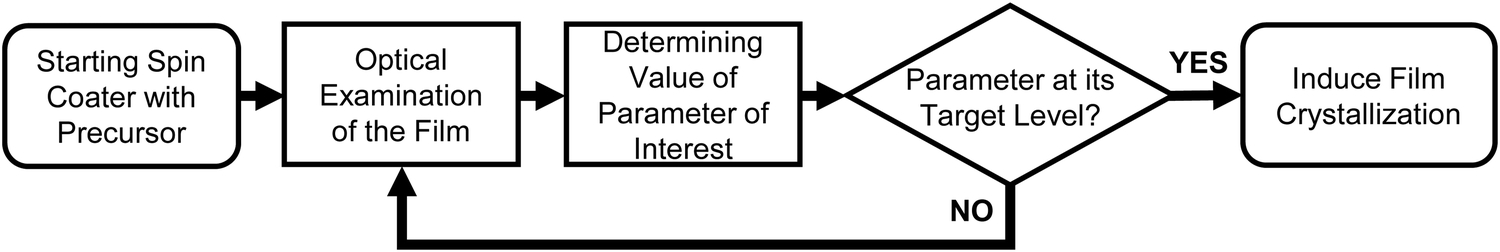 | ||
| Fig. 1 Flowchart of the general scheme of the reactive spin coating procedure. | ||
As mentioned, for demonstration purposes we chose the precursor solution film thickness as the parameter of interest.5,20 For the investigated material system and other commonly used MHP compositions, the parameter thickness d of the precursor solution film can be extracted from an interference pattern that emerges in the absorption spectra between 1.6 eV and 2.4 eV after ≈ 5 s.17,20 This pattern is caused by white light thin-film interference between the upper and lower interface of the precursor solution layer (Fig. 2a)18 and it is spectrally manifested in a sine-like modulation of the otherwise flat absorption spectrum of the precursor solution layer in this energy range. According to Manifacier et al.21 the thickness d of such a film can be calculated by taking advantage of this sinusoidal pattern, using eqn (1):
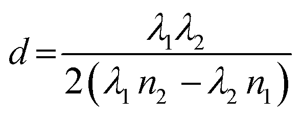 | (1) |
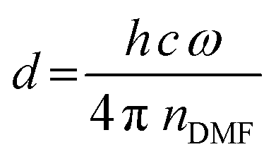 | (2) |
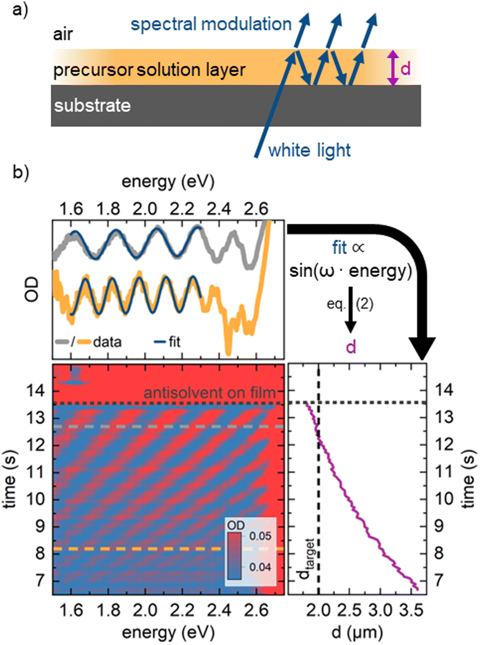 | ||
| Fig. 2 (a) Schematics of the origin of thin film interference pattern used to calculate the film thickness. (b) Depiction of the real-time measurement of solvent layer thickness using in situ absorption spectroscopy (lower left panel). For every time frame (e.g., at the grey/orange dashed lines) a sine-like function is fitted to the absorption data (upper panel) to calculate the solvent layer thickness from the frequency ω of the sine wave using eqn (2). Once this thickness (right panel) decreases below a critical target thickness, the antisolvent is dispensed by an automated syringe pump. | ||
3. Comparing reactive vs. time-based spin coating
To show the capabilities of our approach, we compare the processing of (1) methylammonium lead iodide (MAPbI3, 1.2 M of equimolar lead iodide and methylammonium iodide in DMF) and (2) a mixed cation and halide composition ((MA0.17FA0.83)Pb(I0.83Br0.17)3, 1.2 M in DMF) thin films on glass substrates either via the new reactive or the established time-based spin coating method. We simultaneously record the absorption and PL during the film formation with the optical in situ spin coater setup as described. As the target value for the precursor solution layer thickness, we selected 2 μm since we obtained good MAPbI3 thin films in our previous work when the film was spun at 2000 rpm and the AS was dispensed at this solution layer thickness.5 For the time-based approach, the AS dispensing was initiated 12 s after the start of the spin coating for all spin speeds which corresponds to the time necessary to reach a precursor solution layer thickness of 2 μm for 2000 rpm. To simulate a change in formation kinetics, such as a change in evaporation rate, we varied the spin speed of the spin coater between 2000 and 1250 rpm in 250 rpm steps. This results in a reduction of the solvent evaporation rate constant from 0.21 s−1 for 2000 rpm to 0.15 s−1 for 1250 rpm (for details on the calculation of the evaporation rate constant see Fig. S2, ESI†). First, the recorded in situ data (absorption and PL) are analyzed in more detail to characterize possible differences between the two processing methods that can already be observed during film formation. Then, the optoelectronic properties and morphology of the final films after annealing are investigated and possible differences are identified. Finally, we discuss how the findings obtained from the model system MAPbI3 are translated to the more complex (MA0.17FA0.83)Pb(I0.83Br0.17)3 composition, which is used in high-efficiency perovskite solar cells.43.1 Analyzing the film formation
The 2D heat maps for all MAPbI3 thin films processed via the two spin coating approaches at 2000 and 1250 rpm are shown in Fig. 3 (see Fig. S3 for heat maps of all spin speeds, ESI†). We obtain the familiar optical signatures of perovskite formation as discussed in detail previously.5 In brief, once the AS is dispensed onto the substrate, the expected absorption edge and the perovskite PL signature appear in the absorption channel and the PL channel, respectively. For each spin speed and processing approach we track the peak position of the emerging perovskite PL signal. From this, we calculate the crystallite size for each point in time. This is possible because quantum confinement effects shift the PL peak energy of small crystallites to higher energies compared to values for bulk MAPbI3 (for details on the peak fitting and crystallite size calculation see, eqn (S6) and (S7), ESI†).19,22,23 The obtained crystallite sizes as a function of time are shown in the left panel in Fig. 4a and b. The time t = 0 on the time axes marks the point in time of the AS dispensing. We extract the growth rates for all measurements from linear fits of the crystallite growth after 10 s, with resulting growth rates being shown in Fig. 4c. It is obvious from the plot and the extracted growth rates that for the reactive spin coating, we observe a similar growth rate of perovskite crystallites regardless of the spin speed. In contrast, the obtained growth rates of the samples processed by the time-based method differ significantly between the different spin speeds. For the time-based spin coating, we chose to dispense the AS after spinning for 12 s at 2000 rpm when a precursor solution layer thickness of 2 μm is reached. It is therefore straightforward that the growth rate of the 2000 rpm time-based sample is similar to the 2000 rpm reactive sample. However, when reducing the spin speed in the time-based approach, the growth rate first increases to 0.46 nm s−1 for a spin speed of 1750 rpm and then decreases to 0.325 nm s−1 for 1500 rpm and further to 0.086 nm s−1 for 1250 rpm. Thus, the evolution of the crystallite size already indicates that film formation during the reactive spin coating proceeds in a very similar way independent of the chosen spin speed. In contrast, crystallite growth rates scatter much more when films are processed using the conventional time-based spin coating method.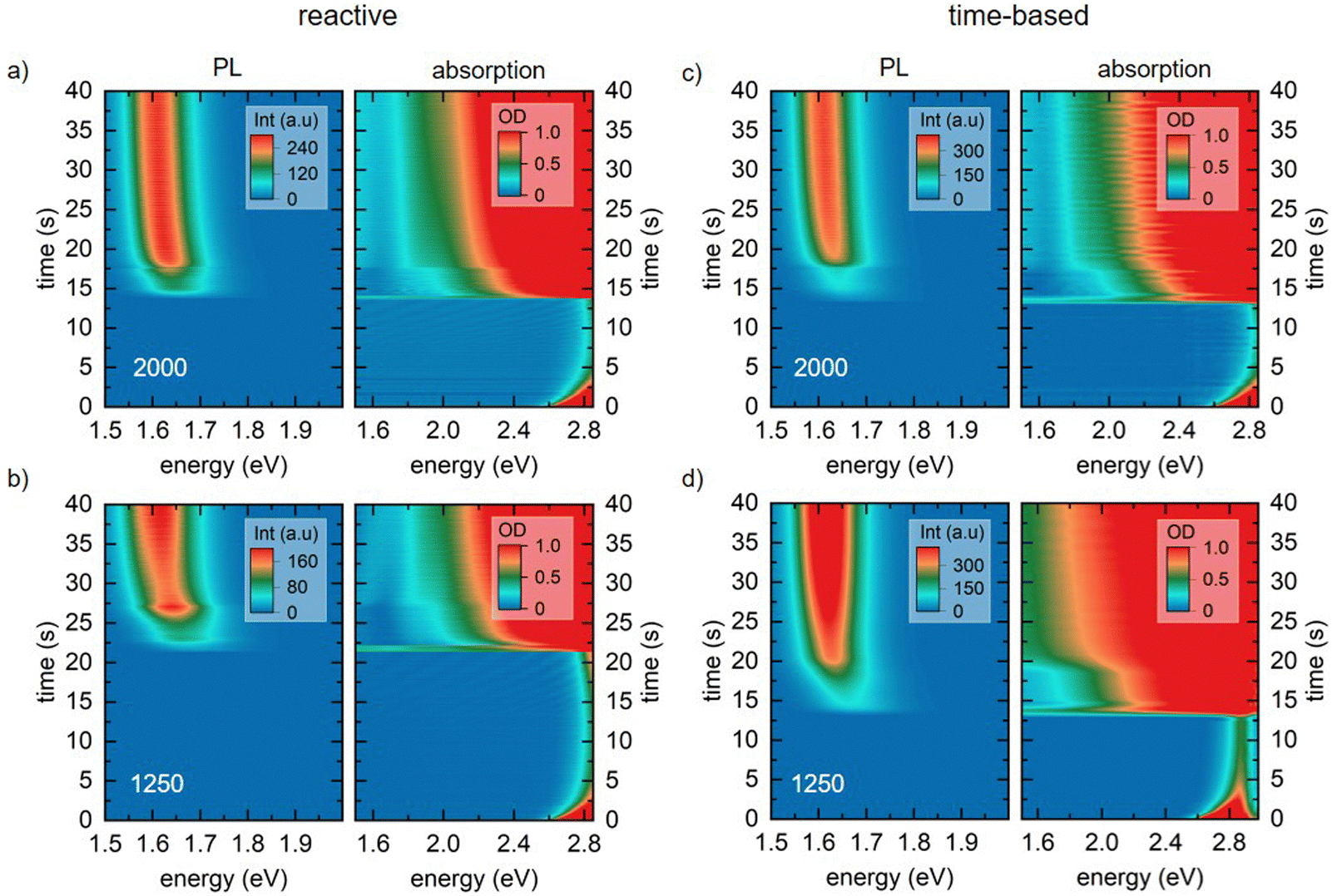 | ||
| Fig. 3 Heat maps of photoluminescence (left) and absorption (right) measurements of MAPbI3 solutions during spin coating via the reactive spin coating approach (a) and (b) and for the time-based approach (c) and (d) for spin speeds of 2000 and 1250 rpm. | ||
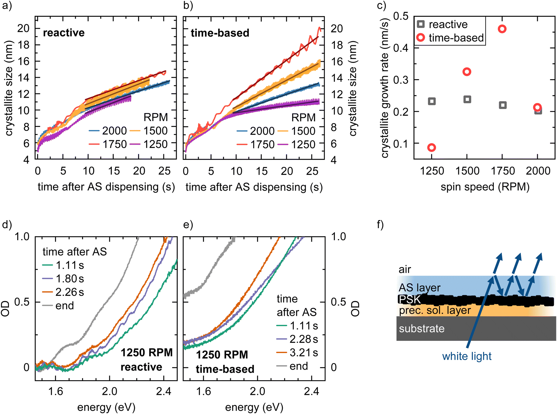 | ||
| Fig. 4 Time evolution of the crystallite size for MAPbI3 films processed via reactive (a) and time-based (b) spin coating for different rpms, extracted from the PL peak position considering quantum confinement. The time axis was shifted that t = 0 corresponds to the time of AS dispensing. (c) Calculated crystallite growth rates for different spin speeds and processing methods, extracted by linear fitting of the evolution of crystallite size over time in (a) and (b). OD spectra at different times during the processing of MAPbI3 films via reactive (d) and time-based (e) spin coating at 1250 rpm. In (d) for 1.11 s and 1.80 s a modulation of the perovskite absorption spectrum is visible. (f) Schematics of the origin of the observed second spectral modulation due to thin film interference after dispensing the AS. | ||
As expected, the initially observed distinct interference pattern of the precursor solution layer in the absorption spectra mostly vanishes as soon as the AS is dispensed, and an absorption edge becomes visible at ∼1.7 eV (Fig. 4d and e). This absorption edge is blue-shifted compared to MAPbI3 bulk values of ∼1.6 eV,18 due to confinement of the forming perovskite crystallites. Interestingly though, at a closer look, we can still observe an interference pattern modulated on top of the signal of the growing perovskite layer for all films processed via reactive spin coating and for most films (2000, 1750, and 1500 rpm) processed via time-based spin coating. For the reactive spin-coated film (Fig. 4d), the interference pattern behaves similarly to the interference pattern of the precursor solution layer, i.e. its modulation frequency decreases with spin coating time. The origin of this additional interference effect is most probably the formation of an AS layer. The AS induces perovskite crystallization and consequently, a perovskite capping layer forms on top of the precursor solution layer. Therefore, excess AS cannot penetrate this capping layer and remains as AS layer on top, causing the observed spectral modulation e.g. between 1.11 und 1.80 s in Fig. 4d (also see Fig. 4f for illustration). Subsequent spinning off and evaporation of the AS layer then leads to the observed decrease in modulation frequency with spin coating time.
The absence of this second interference pattern for the 1250 rpm time-based spin coating suggests that no ‘new’ two-layer system (AS on top of perovskite capping layer) is formed, i.e. the addition of AS was not sufficient to drive the precursor solution into a thermodynamically state allowing for perovskite crystallization.
Furthermore, the significantly more pronounced scattering offset in the absorption spectra in Fig. 4e compared to Fig. 4d, suggests a more inhomogeneous perovskite growth and morphology of the final film processed at 1250 rpm in the time-based approach.
3.2 Comparison of the final film properties
The observations and indications obtained from the data during film formation are confirmed by the analysis of the final films after annealing. As expected from the evolution of crystallite size, the films prepared with reactive processing show an almost identical film structure in cross-section (Fig. 5a) and top view (Fig. S4, ESI†). The film thickness for reactive spin coating is virtually identical for all spin speeds. In contrast, time-based processed films show significant variation. Here, the film thickness is larger the smaller the spin speed. In addition, the existing voids become larger with decreasing spin speed. This confirms the observation during film formation that perovskite first forms on the upper surface of the solution film and then crystallizes downwards towards the substrate. We conjecture that with slower spin speeds and the time-based method, more and more solvent is trapped below the perovskite surface layer, which fully evaporates during the annealing step that follows the spin-coating. The absorption spectra of the reactive spin-coated and the time-based spin-coated series after annealing further substantiate this conclusion: While all films prepared via the reactive spin coating approach show a very similar absorption spectrum, a variation of scattering offset is seen in the films processed via the time-based method (Fig. S5, ESI†).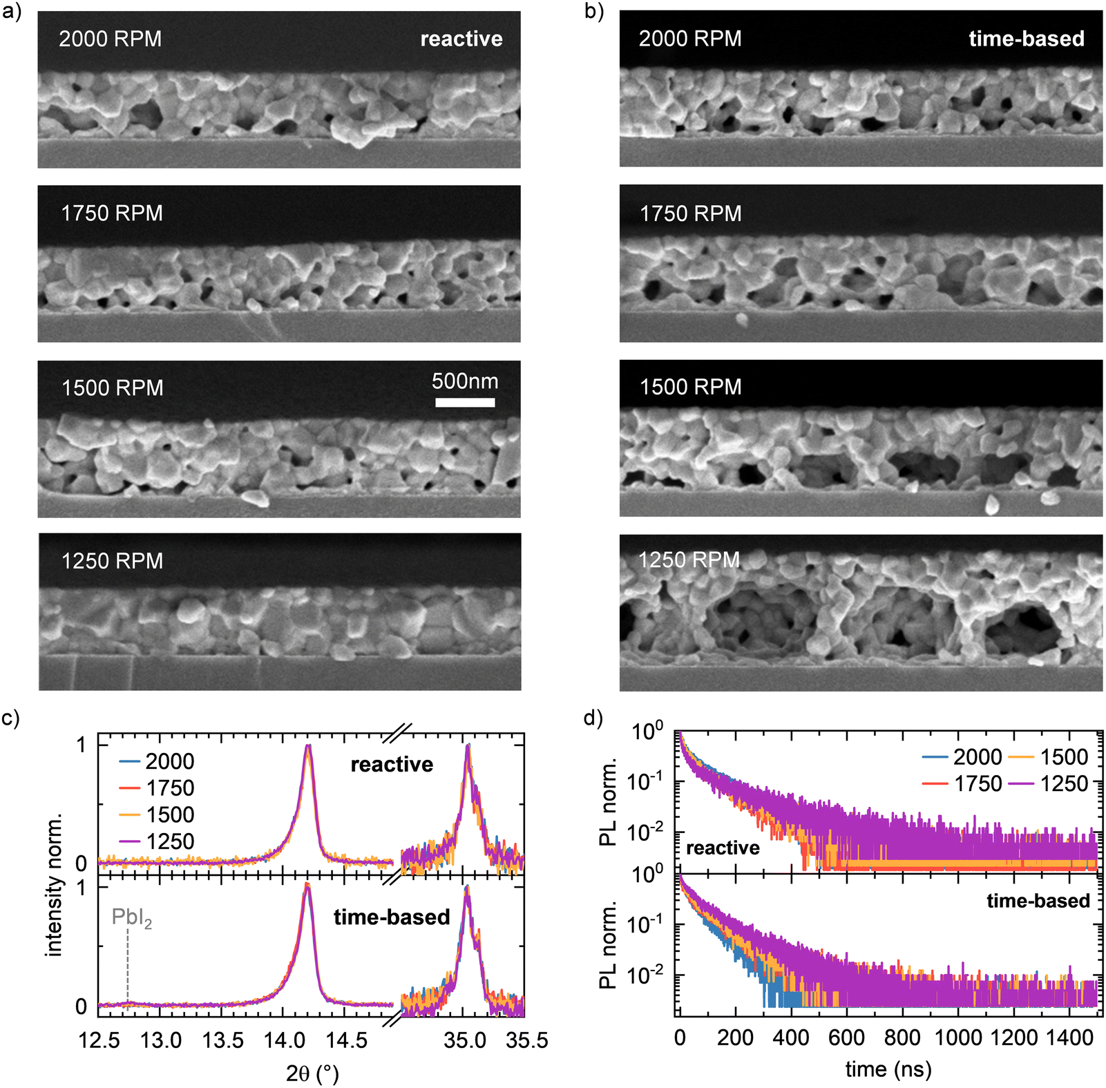 | ||
| Fig. 5 (a) SEM cross-section images of the MAPbI3 films fabricated via reactive spin coating approach at different spin speeds. (b) SEM cross-section images of the MAPbI3 films fabricated via time-based spin coating approach at different spin speeds. (c) XRD peaks of the MAPbI3 films fabricated via reactive (top) or time-based (bottom) spin coating approach at different spin speeds. (d) normalized TRPL curves of the MAPbI3 films fabricated via reactive (top) or time-based (bottom) spin coating approach at different spin speeds. | ||
Both XRD (Fig. 5c and Fig. S6, ESI†) and top view SEM images (Fig. S4, ESI†), as well as steady-state PL spectra (Fig. S5, ESI†) and time-resolved PL (TRPL) curves (Fig. 5d), do not show significant differences between the films prepared by the different methods. This proves that on the length and time scales sampled by PL and XRD, the grain size and the intrinsic properties of the perovskite do not change due to our reactive approach. Additionally, there is no evidence of residual PbI2 present in XRD pattern for all reactive spin-coated films, indicating that the reactive spin coating method robustly yields phase-pure films with uniform film thickness and quality independent of spin speed, whereas small signals of unreacted PbI2 are visible in the XRD pattern in the case of time-based spin coating at spin speeds of 1500 rpm and 1250 rpm. Therefore, we conclude that the reactive approach does not affect the intrinsic morphological properties such as grain size and shape, but our approach preserves these properties independently of the spin speed throughout the perovskite layer.
In addition to the model system MAPbI3, we also investigated if and how the reactive processing approach can be transferred to more complex mixed compositions, such as (MA0.17FA0.83)Pb(I0.83Br0.17)3. The corresponding in situ data and detailed discussions of the measurements can be found in Section 3 in the ESI.† In brief, this mixed system indeed behaves similar to the model system MAPbI3 so far discussed and the final films obtained are comparable to the MAPbI3 layers. In particular, the SEM cross section images (see Fig. 6 and Fig. S10, ESI†) show that also for the mixed (MA0.17FA0.83)Pb(I0.83Br0.17)3 composition, the resulting perovskite layer morphology remains independent of the spin speed for the reactive approach. In contrast, in the time-based approach the perovskite layers exhibit increasingly bigger voids with decreasing spin speed. These findings indicate that the reactive spin coating approach is not only limited to a ternary halide perovskite composition such as MAPbI3, but also transfers to more complex, mixed compositions such as (MA0.17FA0.83)Pb(I0.83Br0.17)3.
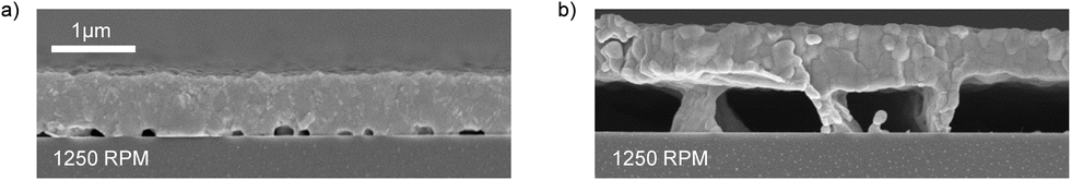 | ||
| Fig. 6 (a) SEM cross-section images of the (MA0.17FA0.83)Pb(I0.83Br0.17)3 films fabricated via reactive spin coating approach at 1250 rpm. (b) SEM cross-section images of the (MA0.17FA0.83)Pb(I0.83Br0.17)3 films fabricated via time-based spin coating approach at 1250 rpm. | ||
4. Conclusion
In summary, the reactive spin coating approach presented here allows to automatically dispense the AS when a certain parameter value, such as precursor solution layer thickness, has been reached, based on the live feedback from the real-time analysis of the optical spectra during spin coating. As a result, films with the same quality (crystallite size, microstructure, and film thickness) could be produced, down to spin speeds as low as 1250 rpm without any additional optimization steps for the model system MAPbI3 as well as for the mixed (MA0.17FA0.83)Pb(I0.83Br0.17)3 composition.To substantiate the advantages of our newly developed method, we compared our new approach with a conventional time-based method, in which the AS is dispensed after a fixed time, leading to a clear variation in the crystallization behavior and differences in the final film properties depending on the spin speed. We emphasize that the reactive spin coating technique is not limited to the precursor solution layer thickness as a parameter of interest, but it can also be easily adapted to other parameters accessible by optical spectroscopy, such as the various PbIx-related precursor absorption peaks that change during spin-coating.
Additionally, our approach enables fundamental film formation studies that rely on the variation of system- and process-internal parameters during film formation (e.g. influence of the properties of PbIx species upon AS addition on the perovskite crystallization process), without the need to rely on variation of system- and/or process-external parameters (e.g. variation of moment of AS dripping, or (external) variation of precursor concentration). This likely will allow a more direct and simplified understanding of the complicated relationship between solution properties and final film properties of halide perovskites.
Thus, our reactive spin coating approach will open up future possibilities to simplify the transfer of recipes from one laboratory to the next by removing the influence of external effects, such as atmosphere or the human factor, on the layer formation as the processing is only based on system-internal parameters. Eventually, our approach also represents a valuable contribution for an in general improved process control in the solution processing of halide perovskite thin films, making it relevant for their successful upscaling and commercialization in optoelectronic devices in the future.
Experimental details
Precursor solution
All materials were used as received. Lead(II) iodide (PbI2, 98%), methylammonium iodide (MAI, 99%), formamidinium iodide (FAI, 99%), lead bromide (PbBr, 99%) and methylammonium bromide (MABr, 99%) were purchased from TCI. For MAPbI3 solutions, PbI2 and MAI were weighed in a stoichiometry of 1![[thin space (1/6-em)]](https://www.rsc.org/images/entities/char_2009.gif) :1 and dissolved in DMF (Acros) to obtain stock solution with a concentration of 1.2 M. For the (MA0.13FA0.83)Pb(I0.83Br0.17)3 solutions, PbI2, FAI, PbBr and MABr were weighed accordingly to obtain a stoichiometry of (MA0.17FA0.83)Pb(I0.83Br0.17)3 and the precursor were dissolved in DMF to obtain a concentration of 1.2 M.
:1 and dissolved in DMF (Acros) to obtain stock solution with a concentration of 1.2 M. For the (MA0.13FA0.83)Pb(I0.83Br0.17)3 solutions, PbI2, FAI, PbBr and MABr were weighed accordingly to obtain a stoichiometry of (MA0.17FA0.83)Pb(I0.83Br0.17)3 and the precursor were dissolved in DMF to obtain a concentration of 1.2 M.
Thin film fabrication
The precursor solutions were spin coated on glass substrates at various spin speeds as detailed in the main text. After the spin coating step, the films were annealed on a hot plate at 100 °C for 10 min.In situ setup
All optical in situ data were recorded with a home-built setup. In brief, photoluminescence and absorption were recorded alternating frame-by-frame at a frame rate of 15 Hz. To ensure reproducibility we recorded at least two coatings for each sample, which turned out to be quasi-identical. Further details are given in the ESI.†XRD
The powder XRD pattern was recorded on a Bragg–Brentano-type diffractometer (Empyrean, Malvern Panalytical BV, Netherlands) equipped with a PIXcel-1D detector using Cu-Kα radiation (λ = 1.5419 Å)REM
The film morphology was characterized by SEM using a Zeiss Leo 1530 instrument FE-SEM with Schottky-field-emission cathode, In-lens detector, and SE2 detector. The accelerating voltage was 3 kV. Prior to measurement, the samples were sputtered with 2 nm platinum.TRPL
For time-resolved photoluminescence curves, time-correlated single-photon counting (TCSPC) measurements were performed with a PicoQuant MT200 confocal fluorescence microscope in combination with a PMA Hybrid PMT 40 photomultiplier tube (PicoQuant) and a TimeHarp 260 Pico TCSPC board (PicoQuant). The samples were excited with a 560 nm diode Laser (PicoQuant LDH-D-TA-560) with a frequency of 2.0 MHz and a pulse width of 68 ps. The laser beam was focused on the sample with an Olympus Objective with 4× magnification, and the emission was filtered with a 561 nm long-pass filter before detection. The excitation fluence was set to 300 nJ cm−2.Conflicts of interest
There are no conflicts to declare.Acknowledgements
The authors acknowledge financial support from the German National Science Foundation DFG via the projects PA 3373/3-1, MO 1060/32-1, PA 3373/6-1, KO 3973/3-1, GR 5505/3-1 and the IRTG 2818 OPTEXC. We also thank Martina Heider and the KeyLabs “Electron and Optical Microscopy” and “Device Engineering” of the Bavarian Polymer Institute (BPI) for assistance with SEM images and access to the MT200 system. Further, we want to thank Christopher Greve for assistance with XRD measurements and Philipp Ramming for assistance with the TRPL measurements.References
- NREL, Best Research-Cell Efficiency Chart, https://www.nrel.gov/pv/cell-efficiency.html, accessed February 15, 2024.
- Q. Cao, Y. Li, H. Zhang, J. Yang, J. Han, T. Xu, S. Wang, Z. Wang, B. Gao, J. Zhao, X. Li, X. Ma, S. M. Zakeeruddin, W. E. I. Sha, X. Li and M. Grätzel, Sci. Adv., 2021, 7, eabg0633 CrossRef CAS PubMed.
- Y. Zhao, T. Heumueller, J. Zhang, J. Luo, O. Kasian, S. Langner, C. Kupfer, B. Liu, Y. Zhong, J. Elia, A. Osvet, J. Wu, C. Liu, Z. Wan, C. Jia, N. Li, J. Hauch and C. J. Brabec, Nat. Energy, 2022, 7, 144–152 CrossRef CAS.
- M. Saliba, J.-P. Correa-Baena, C. M. Wolff, M. Stolterfoht, N. Phung, S. Albrecht, D. Neher and A. Abate, Chem. Mater., 2018, 30, 4193–4201 CrossRef CAS.
- S. Biberger, K. Schötz, P. Ramming, N. Leupold, R. Moos, A. Köhler, H. Grüninger and F. Panzer, J. Mater. Chem. A, 2022, 10, 18038–18049 RSC.
- K. P. Goetz and Y. Vaynzof, ACS Energy Lett., 2022, 7, 1750–1757 CrossRef CAS.
- Y. Zou, Y. Li, X. Pang, Y. Song, W. Xu and B. Sun, J. Phys. Chem. Lett., 2023, 14, 5025–5032 CrossRef CAS PubMed.
- O. Shargaieva, H. Näsström, J. A. Smith, D. Többens, R. Munir and E. Unger, Mater. Adv., 2020, 1, 3314–3321 RSC.
- A. D. Taylor, Q. Sun, K. P. Goetz, Q. An, T. Schramm, Y. Hofstetter, M. Litterst, F. Paulus and Y. Vaynzof, Nat. Commun., 2021, 12, 1878 CrossRef CAS PubMed.
- K. Wang, M.-C. Tang, H. X. Dang, R. Munir, D. Barrit, M. De Bastiani, E. Aydin, D.-M. Smilgies, S. De Wolf and A. Amassian, Adv. Mater., 2019, 31, 1808357 CrossRef PubMed.
- Q. An, L. Vieler, K. P. Goetz, O. Telschow, Y. J. Hofstetter, R. Buschbeck, A. D. Taylor and Y. Vaynzof, Adv. Energy Sustainability Res., 2021, 2, 2100061 CrossRef CAS.
- T.-B. Song, Z. Yuan, F. Babbe, D. P. Nenon, E. Aydin, S. De Wolf and C. M. Sutter-Fella, ACS Appl. Energy Mater., 2020, 3, 2386–2393 CrossRef CAS.
- A. M. Valencia, O. Shargaieva, R. Schier, E. Unger and C. Cocchi, J. Phys. Chem. Lett., 2021, 12, 2299–2305 CrossRef CAS PubMed.
- D. E. Bornside, C. W. Macosko and L. E. Scriven, J. Electrochem. Soc., 1991, 138, 317 CrossRef CAS.
- J. Danglad-Flores, S. Eickelmann and H. Riegler, Eng. Rep., 2021, 3, e12390 CrossRef CAS.
- M. Buchhorn, S. Wedler and F. Panzer, J. Phys. Chem. A, 2018, 122, 9115–9122 CrossRef CAS PubMed.
- H.-S. Yun, H. W. Kwon, M. J. Paik, S. Hong, J. Kim, E. Noh, J. Park, Y. Lee and S. I. Seok, Nat. Energy, 2022, 7, 828–834 CrossRef CAS.
- M. Chauhan, Y. Zhong, K. Schötz, B. Tripathi, A. Köhler, S. Huettner and F. Panzer, J. Mater. Chem. A, 2020, 8, 5086–5094 RSC.
- L. Polavarapu, B. Nickel, J. Feldmann and A. S. Urban, Adv. Energy Mater., 2017, 7, 1700267 CrossRef.
- K. Schötz, C. Greve, A. Langen, H. Gorter, I. Dogan, Y. Galagan, A. J. J. M. van Breemen, G. H. Gelinck, E. M. Herzig and F. Panzer, Adv. Opt. Mater., 2021, 9, 2101161 CrossRef.
- J. C. Manifacier, J. Gasiot and J. P. Fillard, J. Phys. E: Sci. Instrum., 1976, 9, 1002–1004 CrossRef CAS.
- J. A. Sichert, Y. Tong, N. Mutz, M. Vollmer, S. Fischer, K. Z. Milowska, R. García Cortadella, B. Nickel, C. Cardenas-Daw, J. K. Stolarczyk, A. S. Urban and J. Feldmann, Nano Lett., 2015, 15, 6521–6527 CrossRef CAS PubMed.
- Y. Kayanuma, Phys. Rev. B: Condens. Matter Mater. Phys., 1988, 38, 9797–9805 CrossRef PubMed.
Footnote |
| † Electronic supplementary information (ESI) available. See DOI: https://doi.org/10.1039/d3tc04361d |
| This journal is © The Royal Society of Chemistry 2024 |