
 Open Access Article
 This Open Access Article is licensed under a
 Creative Commons Attribution 3.0 Unported Licence
On-chip organic optoelectronic system for fluorescence detection†
Emilia
Benvenuti
a,
Andrea
Lanfranchi
 b,
Salvatore
Moschetto
a,
Marco
Natali
a,
Marco
Angelini
c,
Paola
Lova
b,
Federico
Prescimone
a,
Vincenzo
Ragona
a,
Davide
Comoretto
b,
Mario
Prosa
*a,
Margherita
Bolognesi
a and
Stefano
Toffanin
*a
b,
Salvatore
Moschetto
a,
Marco
Natali
a,
Marco
Angelini
c,
Paola
Lova
b,
Federico
Prescimone
a,
Vincenzo
Ragona
a,
Davide
Comoretto
b,
Mario
Prosa
*a,
Margherita
Bolognesi
a and
Stefano
Toffanin
*a
aInstitute of Nanostructured Materials (ISMN), National Research Council (CNR), Via P. Gobetti 101, Bologna 40129, Italy. E-mail: mario.prosa@cnr.it; stefano.toffanin@cnr.it
bUniversity of Genoa, Department of Chemistry and Industrial Chemistry, Via Dodecaneso 31, Genoa 16146, Italy
cOptics For Life, Via Roma 67, Trivolzio 27020, Italy
First published on 26th February 2024
Abstract
Conventional fluorescence sensing, despite its high sensitivity, is poorly suited for point-of-need applications due to the bulkiness and cost constraints of standard components. An urgent market demand exists for integrated, portable, and high-performance solutions. Here, an efficient and miniaturized fluorescence sensor is demonstrated by innovative integration on a single substrate of organic optoelectronic devices, such as an organic photodiode and an organic light-emitting diode, with a polymeric distributed Bragg reflector. Optical modeling of the 3D layout of integration of the three all-organic components allows maximizing the optical efficiency of the sensing system, which outperforms that of state-of-the-art miniaturized fluorescence sensors by two orders of magnitude. Accordingly, fluorescence signals from microfluidic volumes of Rhodamine 700 are detected by the sensor over a wide range of dye concentrations, ranging from 10−3 M to 10−6 M. The optimized exploitation of the angular dependence of the distributed Bragg reflector filter characteristics provides a remarkable reduction of the undesired optical signal of excitation. As a result, a significant increase of the signal-to-noise ratio allows for halving the detection limit of Rhodamine 700 down to 9.2 μM, thus demonstrating the possible implementation of such innovative integrated detection scheme for biodiagnostics.
Introduction
Sensors are intelligent solutions for numerous life-related applications, ranging from food quality and safety analysis to environmental monitoring. In this context, fluorescence sensing is a reference method for the detection of a plethora of different compounds including biomolecules and metal ions.1In fluorescence sensing, a light source and a light detector are respectively involved to excite a dye-labelled analyte and to detect the fluorescent signal to analyse. Conventional fluorescence sensing systems are very sensitive, but they are typically bulky, complex, and expensive since they are based on benchtop optical components such as lasers, photomultiplier tubes, or fluorescence microscopes.2 Therefore, the methodology is usually confined to analytical labs, thus limiting its application to occur far from the point-of-need (PON) and restricting the use to trained personnel.
Nowadays, there is the urgent need to transfer lab-confined technologies into the site of analysis in order to provide rapid analytical and diagnostic feedback directly in the PON proximity.3 In this context, the typical low detection limits of conventional fluorescence equipment need to be guaranteed while moving towards integrated, miniaturized, and even on-chip detection modules to be used reliably and everywhere.
Highly integrated sensors such as lab-on-a-chip systems combining optical, optoelectronics, and microfluidic elements on the same substrates are attracting great interest.4 Recent advances in the smart-system integration of optoelectronic devices allowed for the development of a plethora of portable sensors ranging from wearable oximeters to fully integrated and self-powered sensors with multiple capabilities.5–7
In this context, optoelectronic devices based on organic semiconductors, thanks to their ease and versatility of processing by low temperature techniques,8,9 and the possibility to be deposited also on plastic and flexible substrates, represent valid candidates in realizing miniaturized and cost-effective photonic systems.10 A great modulation of the optoelectronic features of the devices is further provided via a targeted design and synthesis of the compounds.11–15 Through the smart integration of organic optoelectronic devices such as organic light-emitting diodes (OLEDs) and photodiodes (OPDs), and a nanostructured metal film, we have recently demonstrated an ultra-compact system endowed with plasmonic sensing capabilities to assess rapid and on-site analysis at a quality level comparable to that of laboratory tests.16,17
Similarly, several examples of miniaturized fluorescence sensors based on the integration of organic optoelectronic devices have been reported in literature. In particular, the two main components of the sensor, i.e. the light excitation source and the photodetector, are typically OLEDs and OPDs with customized shapes which are suitably integrated monolithically on a substrate18 or stacked vertically to provide efficient and cooperative operation.19–23 The third basic component is the sensing element, that is a luminescent compound whose optical properties change upon interaction with the analyte of interest.24
One of the most common detection schemes is based on a reflection-type configuration in which the optoelectronic platform, including OLEDs and OPDs, triggers the fluorescence emission of a luminescent sensing film placed on the top side.25 A quantitative analysis is performed as a function of the amount of exposed analyte. Although transmission-type detection schemes have been also realized, the face-to-face architecture where the light source and the light detector are vertically stacked on each other is typically affected by a large background noise due to the direct illumination of the light detector by the OLED excitation light, which overshadows the fluorescent signal. Nevertheless, this issue is not fully avoided in reflection-type schemes and it is still limiting the signal-to-noise ratio.22,25 The excitation light is indeed orders of magnitude more intense than the fluorescence signal, and still a relevant amount typically reaches the OPD as it is only partially absorbed by the fluorophore.
A possible approach to overcome this type of issues is to tune the spectral characteristics of the optoelectronic devices to avoid the direct interaction between the OLED and the OPD. Either narrowing the emission spectrum of OLEDs24,26 or developing spectrally selective OPDs are complex approaches that involve a modification of the device structure.5 Alternatively, the detection scheme of the sensor can be suitably designed to avoid the OLED light to reach the OPD as, for instance, by using complex architectures exploiting waveguide effects.27
Diversely, in commercial instruments, this type of issues is typically avoided by inserting optical filters in front of the detector to reject light in the excitation spectral region and to transmit that in the fluorophore emission spectral region.28
Some works reported on the application of such strategy into miniaturized sensors. However, the complex integration required a simplification of the assembly of the system that was obtained by coupling OLEDs, OPDs, and optical filters as independent components.29–32 This approach led to a suboptimal optical efficiency as a result of the multiple interfaces existing between the composing elements.
Here, we report the unprecedented combination of organic optoelectronic devices with a polymeric optical stop-band filter, onto the same substrate, as an all-organic on-chip integrated fluorescence sensor. The components and the layout of integration are suitably designed to make the three elements work cooperatively in a reflection-type configuration, in which an OLED is fabricated onto the polymeric stack of the optical filter, and it is laminated onto an OPD. In this view, an optical simulation model is developed to effectively design the 3D layout of the fluorescence sensing architecture. The ultra-compact vertical stack of components allows for easy integration of the microfluidic system on the top-side, thus avoiding possible issues arising from the turbidity of real samples.
As the optical filter, an all-organic distributed Bragg reflector (DBR) is developed via the alternated deposition of solution-processed layers of polymers having different refractive indices. The spectral characteristics of the DBR filter are tailored to guarantee both optical filtering of the backscattered excitation light and transmission of the dye fluorescence to the OPD. The optical performance of polymer DBRs have been demonstrated in several photonic fields.33–35 The strong angle-dependent characteristics of the DBR filter is one of the key-enabling factors that allows to reach high sensing performance once the correct layout of integration is identified. Optical simulations are implemented, considering angle- and wavelength-dependent efficiencies of all components, to determine the optimal size and relative positioning of the elements in the integrated system, as well as to predict the output signal from the sensor. The sensing performance of the final miniaturized sensor, fabricated according to the optimized design, is validated by analysing the output signal of the sensor in response to microfluidic volumes of the model dye Rhodamine 700 (a widely used dye for biotechnology applications) at variable concentrations ranging from 10−3 M to 10−6 M.
Results and discussion
Fig. 1a shows the concept of the all-organic on-chip integrated fluorescence sensor. To optimize the fluorescence detection in a reflection-mode scheme, the proposed architecture minimizes the lateral distance between the light source and the light detector by stacking all active components rather than using the traditional side-by-side configuration. Specifically, the OLED is directly fabricated on top of the OPD, while the DBR filter is integrated in between them. In the principle of operation, the fluorescent sample is placed at the top of the system, and it is excited by a top-emitting OLED light source. The isotropic fluorescence emission arising from the sample is collected by a top-absorbing OPD placed beneath the OLED and spanning over a larger area at the sides of the OLED. The DBR filter prevents the backscattered excitation light to be detected, while it transmits the fluorescence signal to the OPD.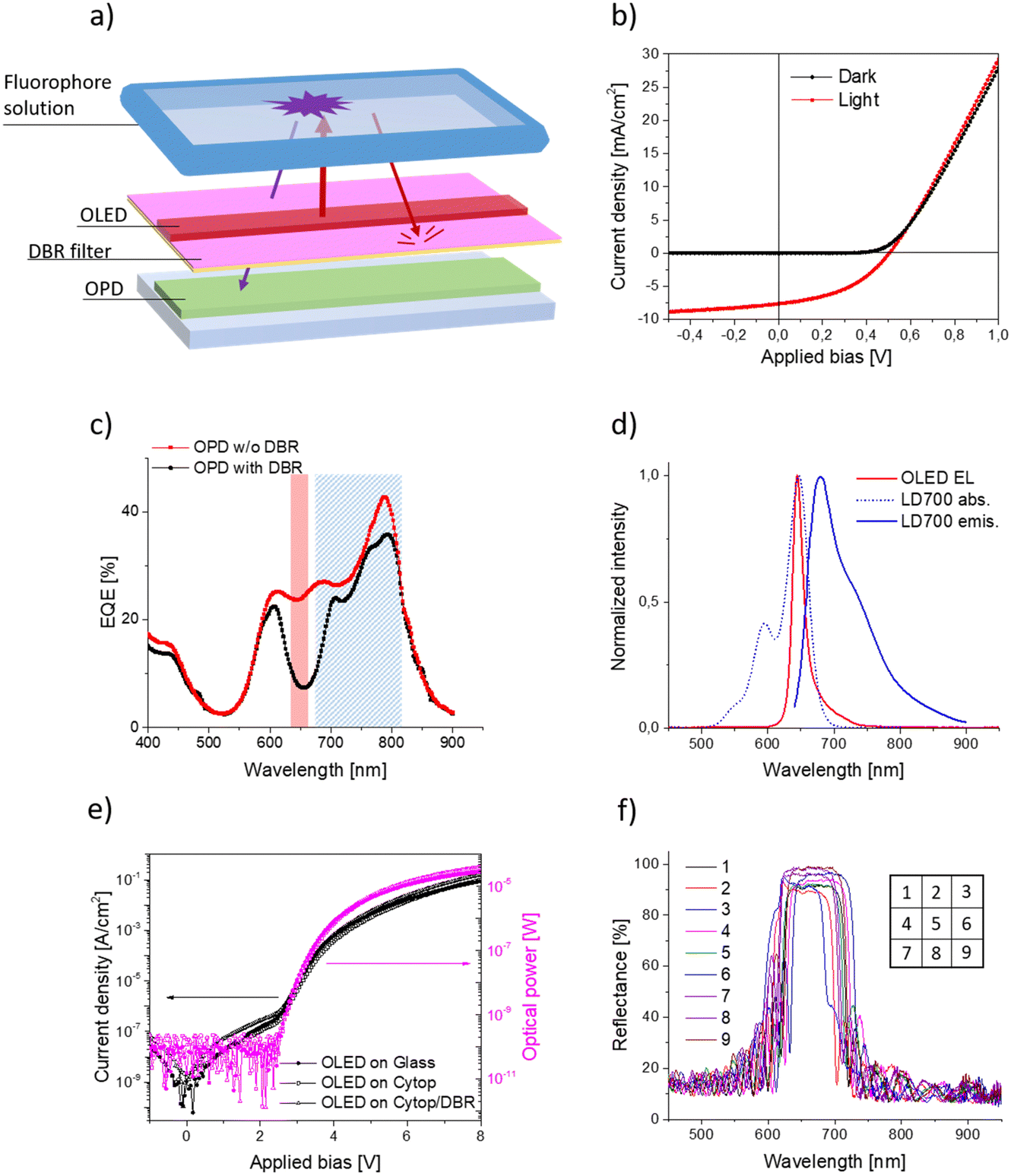 | ||
| Fig. 1 (a) Simplified representation of the proposed fluorescence sensor. (b) Current density vs. applied voltage plot (J–V plot) of the OPD measured in dark conditions (black dots) and under light illumination (red dots). (c) External quantum efficiency (EQE) of a pristine OPD (red line) and of a spectrally selective OPD (black line) obtained by integration of the DBR optical filter. The red area highlights the spectral region of OLED emission, the blue area the spectral region of the fluorescence emission of LD700. (d) Normalized electroluminescence spectrum of the Pt(OEP)-based OLED (red line), absorption (dotted blue line) and emission (solid blue line) spectra of LD700 in ethanol. (e) Current density (black lines) with the corresponding power of emission (pink line) for OLED fabricated on glass (solid line), on Cytop (squares), on DBR filter (triangles). (f) Reflectance spectra of the DBR filter fabricated on a PET substrate; coloured lines refer to measurements on different regions of the 25 × 25 mm2 sample as shown in the inset. | ||
For the validation of the fluorescence sensing operation, Rhodamine 700 (LD700) was identified as a suitable model dye due to the large use of Rhodamine-based fluorophores in bio-imaging and bio-diagnostics.36 In addition, spectral features such as the small Stokes shift of 32 nm is also similar to that of other fluorescent molecules which are used for cell labelling.37 Before fabricating the integrated fluorescence system, the organic optoelectronic components were designed so to have well matched optical and spectral characteristics. The composing elements were first optimized by fabrication on independent substrates. A blend of zinc phtalocyanine and fullerene was selected as active layer of the OPD, due to the wide spectral response in the visible range that is suitable to detect the fluorescence emission of LD700.38,39 A top-adsorbing OPD structure (Fig. S1a, ESI†) was optimized in terms of electrical and optical characteristics by tuning the type and thickness of interlayers and by introducing a refractive index matching layer (IML) onto the semi-transparent cathode to obtain a device that is highly sensitive at the peak wavelength of emission of LD700, that is 680 nm (Fig. 1d). Good diode-like characteristics were measured in both dark and light conditions (Fig. 1b). Under AM1.5G illumination, the OPD showed a short-circuit photogenerated current density (JSC) of 7.5 mA cm−2 and an open-circuit voltage (VOC) of 0.5 V, in agreement with literature.38,39 As a result, the detectivity (D*) resulted to be 1.2 × 10¹¹ Jones at −0.4 V. These data highlight the high device quality, which allows to efficiently drive the OPD at 0 V during light sensing, without the need to operate under reverse bias to ensure high performance. The achievement of the desired spectral response was evidenced in the external quantum efficiency (EQE) spectrum, that covers the range of wavelengths between 610 and 800 nm with values over 25% at 680 nm and a maximum response at 790 nm, which allows recording the full emission of LD700 (Fig. 1c). In addition, the linearity of the OPD response as a function of light intensity was also verified (Fig. S2, ESI†). As the light source of the system, a top-emitting OLED based on the platinum octaethylporphyrin (Pt(OEP)) complex was developed. Compared to other state-of-the-art dopants of host:guest emissive layers, Pt(OEP) provides an efficient and narrow phosphorescent emission with a typical full width at half maximum (FWHM) of a few tens of nm.40,41 In accordance with literature, the electroluminescence spectrum of the developed OLED presents a maximum of emission at 644 nm with a FWHM of 20 nm (Fig. 1d). While the emission maximum perfectly overlaps with the absorption spectrum of LD700, the narrow FWHM facilitates the development of the stop-band DBR filter with not-strict requirements on the bandwidth. The OLED stack was developed to enable the light emission from the top side, thus comprising a reflective Ag layer as the bottom anode electrode and a semitransparent top cathode electrode (Fig. S1b, ESI†). As in the case of OPD, the structure was optimized by the fine tuning of the composition and thickness of the interlayers, and by including an organic IML to favor light extraction from the top of the device. The commercial software SETFOS42 provided by Fluxim was used to simulate and to optimize the OLED architecture in terms of spectral shape and intensity of emission (Fig. S3, ESI†). Fig. 1e shows the optoelectronic characteristics of the OLED fabricated following the simulations. The performance of the OLED results at the state-of-the-art for similar devices,43 reporting a turn-on voltage of 2.5 V and an optical power of 15.0 ± 3.2 μW at a current density of 31 mA cm−2 that is reached by driving the device at 6.7 ± 0.1 V.
The DBR optical filter was developed on a 0.125 mm-thick adhesive polyethylene terephthalate (PET) substrate. The use of solution processable materials and of a thin, transparent and flexible substrate enables the easy integration and adhesion of the DBR filter onto the OPD. The spectral requirements of the DBR filter were optimized to have an optical rejection of at least 90% (for the suitable angle) in correspondence of the emission peak of the OLED, and a transmission above 90% in the spectral region of the fluorescence signal (above 700 nm, Fig. 1f). The materials selected for the DBR filter to respond to the above requirements are the two polymers Aquivion® (AQ) and poly(N-vinylcarbazole) (PVK), which have refractive indexes of 1.3444 and 1.68,45 respectively. The thickness of the deposited layers was around 120 nm and 97 nm, as calculated by numerical modeling.35 The combination of 20.5 AQ/PVK bilayers allowed to reach an optimal trade-off between a sufficiently low complexity of the DBR filter processing and a maximized rejection efficiency. The homogeneity of the structure was relatively good, as indicated by the similar reflectance spectra collected in various regions of the filter (Fig. 1f). The FWHM resulted to be around 100 nm. The difference in peak intensity is due to the difficulty of optically focusing the curved sample in the normal incidence setup. Calculations of theoretical spectra reported in Fig. S6a (ESI†) suggest that the actual peak reflectance should be that of spots 7–9 of Fig. 1f, over 95%. Little spectral variations of shape and spectral position of the rejection region on different spots of the sample can be also ascribed to layer thickness fluctuations arising from solution processing on a flexible substrate.
As a preliminary test, we evaluated the efficiency of the DBR filter when coupling it to the OLED, both as standalone elements, in transmission configuration. The integrated spectrum of emission of the OLED showed an overall reduction of about 78% after passing through the DBR filter (Fig. S4, ESI†). Taking into account that contributions from different wavelengths around the peak should be considered, the overall rejection of the OLED emission by the DBR filter was expected to be below 90%.
A thin layer of Cytop®, an optically transparent and electrically insulating perfluorinated polymer, was first deposited onto the OPD, to guarantee a good adhesion and a low surface roughness for the DBR filter integration. The Cytop layer also protects the OPD surface from possible unwanted scratches occurring during the DBR integration. The Cytop-planarized OPD surface resulted very homogeneous and flat. The OPD performance was preserved after the Cytop deposition (Fig. S5, ESI†). It is worth noting that the use of a protective polymeric layer on top of the OPD can be considered as propaedeutic step for the direct deposition of the DBR active layers onto the OPD, thus further improving the level of integration of the system. Nevertheless, the fabrication of the DBR filter from solution could affect the performance of the OPD, e.g. through moisture or residual solvent percolation from the DBR layers into the OPD active layers. Instead, the fabrication of the DBR filter on a separate substrate such as thin PET is the best trade-off to guarantee a robust process of integration while avoiding to affect the OPD performance.
The effective integration of the DBR filter on top of the OPD was verified by measuring the spectral response of the resulting integrated system, i.e. the spectrally-selective OPD (Fig. 1c). In correspondence of the DBR rejection band of the DBR filter (at 650 nm), the EQE was reduced to 7%, whereas minor differences were observed in the spectral region of the fluorophore emission (above 700 nm).
The final step prior to the development of the integrated sensor is the check of the OLED functionality and performance once fabricated on top of the multilayered OPD/Cytop/DBR stack. Remarkably, the resulting OLED showed similar performance as the reference OLED on the glass substrate, presenting a voltage of 6.5 ± 0.1 V and an optical power of 15.7 ± 1.7 μW when driven at a constant density current of 31 mA cm−2 (Fig. 1e).
The development of the OPD, the DBR filter, and the OLED allowed to obtain three components with spectral characteristics that are compatible and suitable for the detection of fluorescence signal of LD700 (Fig. 1c and d). Nevertheless, having a good spectral overlap between the optical elements is not sufficient to produce an efficient integrated sensor. The process of system integration also requires a keen analysis of the 3D geometry of the system. For instance, OLEDs are not point-like light sources and their emission is not collimated, therefore the Lambertian angular emission needs to be considered in the design of sensor.16 Consequently, the in-plane dimensions and respective distances of the optical and optoelectronic elements are of pivotal importance for the effective operation of the system.
A simulation tool based on optical ray tracing was used with two main aims: (i) to identify the most effective system-layout; (ii) to simulate the output signal from the sensor under different conditions.
The simulation of the layout comprising light source and light detection, without the optical filter, was first carried out in order to determine the best position and the dimensions of single components and to validate the scheme of detection. Optical and spectral experimental characteristics of the OLED, OPD and fluorophore served as input data of the simulation tool. The simulated vertical-stack suggested the OLED having lateral (x) dimension of 500 μm, that is placed on the top of the OPD extending symmetrically at the sides of the OLED (total lateral dimension of the light-sensing surface: 2200 μm). The proposed layout showed a system efficiency of 0.13% calculated as the ratio between the fluorescence radiation reaching the OPD and the emission power of the OLED. If compared to state-of-the-art sensors22 typically in a side-by-side configuration of OLEDs and OPDs, the accurate design of the system allowed increasing the efficiency by two orders of magnitude, thus confirming the effectiveness of the here proposed system-integration approach.
To verify the effect of the DBR filter on the system operation, the spectral and angular optical responses of the DBR filter were introduced in the simulation tool. Since the spectral response of DBR filter strongly depends on the angle of incidence of the incoming light (Fig. S6, ESI†), the design of the integrated system considered multiple-wavelengths and multiple-angles contributions. Accordingly, the modeled spectrum of the OLED backscattered light impinging on the OPD was analyzed (Fig. 2a).
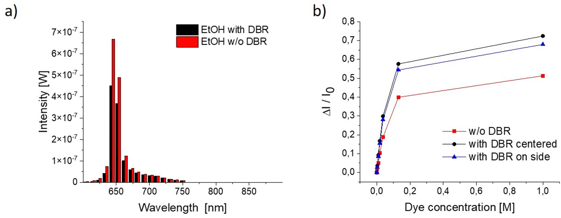 | ||
| Fig. 2 (a) Simulation of the spectral distribution of light reaching the OPD in absence and in presence of the DBR filter, for the system exposed to a reference solvent. (b) Simulations of the output signals of the systems without DBR (red line) and with integrated DBR in different geometries (blue and black lines) in response to different concentrations of LD700 fluorophore in ethanol. | ||
In presence of the DBR filter, a decrease of the optical signal at around 650 nm, that corresponds to the OLED emission peak, was clearly evidenced with respect to the sensor without any optical filters. The spectrum is instead unaffected in the other spectral regions thus confirming the effective operation of the DBR in the integrated system. It is worth noting that the reduction of OLED backscattered signal due to the DBR filter is less pronounced in the integrated system (Fig. 2a) than for the measure made in transmission mode on the independent components (Fig. S4, ESI†). This remarks the importance of simulating the on-chip integrated system considering the full angular characteristics of all the components.
To evaluate the response of the system in a real-case application, the output signal was simulated as a function of fluorophore concentrations ranging from 10−3 M to 10−6 M. The output signal is calculated as ΔI/I0, where ΔI is the difference between the photocurrent of the OPD exposed to the fluorophore solution (I) and the photocurrent of OPD in absence of the fluorophore (exposed to a pure ethanol solution) (I0). As expected, the presence of the DBR improves the output signal in the whole range of LD700 concentrations with respect to the pristine system (Fig. 2b). An in-depth analysis highlights that the beneficial effect of the DBR is more pronounced at low dye concentrations, while decreasing at higher concentrations (Fig. S7, ESI†). This specific behavior likely arises from fluorescence self-absorption occurring in the more concentrated fluorophore solutions. Indeed, this effect cannot be neglected considering the low Stokes-shift of LD700.46 A further proof of such behavior is the trend towards saturation of ΔI/I0 at LD700 concentration above 0.13 mM (Fig. 2b). Before realizing the integrated system, a further step of optimization of the layout was carried out by verifying the optimal in-plane position of the OLED with respect to the OPD. The lateral position of the OLED is expected to have an impact on the system response as a result of the angular dependance of the DBR characteristics. Two different positions were evaluated, one in which the OLED is placed in correspondence of the outermost side of the OPD, the other one in which the OLED is instead located in the middle of the OPD. Fig. 2b shows that a central configuration is the most effective for fluorescence detection, as highlighted by the increased ΔI/I0 at each LD700 concentration.
Based on the output of simulations, the on-chip integrated system was fabricated (Fig. 3 and Fig. S1c, ESI†).
 | ||
| Fig. 3 Schematic representation (top side) and relative pictures (bottom side) of all steps involved in the fabrication process of the on-chip organic optoelectronic system for fluorescence detection. In details, 6 OPDs (green stripes) are fabricated onto a glass substrate (a); a layer of Cytop (yellow) is spin-coated onto the OPDs for electrical insulation (b); a DBR filter (violet) is first fabricated on a plastic substrate and, through a peel-off transfer process, it is then laminated onto the OPDs+Cytop platform (c); 6 OLEDs (red stripes) are fabricated on top of the resulting platform, each corresponding to 1 OPD, to obtain the on-chip integrated fluorescence system (d). | ||
In view of real-setting applications when multiple samples are typically analysed simultaneously, the number of sensors on a single substrate was maximized. Therefore, 6 identical integrated systems, each including the OPD, the DBR filter and the OLED, were fabricated on a substrate, and a microfluidic chamber with a volume of 350 μL was placed on top of it. In details, 6 OPDs were thermally deposited onto a glass substrate; a layer of Cytop was spin-coated onto the OPDs for electrical insulation; a DBR filter was first fabricated on a plastic substrate and then laminated onto the OPDs+Cytop platform via a peel-off transfer process; 6 OLEDs were eventually fabricated on top of the resulting platform, each corresponding to 1 OPD, to obtain the on-chip integrated fluorescence system.
To verify the system operation, the signal from the on-chip integrated system in response to solutions of LD700 at concentrations from 0.05 mM to 1 mM was recorded (Fig. 4a). Pure ethanol was used as the reference medium. The measurements were carried out by driving the OLED at a constant density current (31 mA cm−2) and recording the OPD photocurrent over time during the sequential flow of the different solutions in the microfluidic chamber. As shown in Fig. 4a, an increase of the OPD photocurrent is observed in response to solutions at increasing dye-concentrations, thus demonstrating the ability of the sensor to detect fluorescence signals. Specifically, the background photocurrent signal I0, recorded in absence of fluorophore molecules (in response to the reference pure ethanol), amounted to 270 nA, while an increase by about 100 nA was recorded when introducing 0.05 mM LD700 in the microfluidic system. The non-negligible background is due to the residual OLED light that is backscattered by the microfluidic wall and it is not completely stopped by the DBR filter, thus reaching the OPD.
 | ||
| Fig. 4 (a) Experimental data of the photocurrent generated by the OPD over time when the fluorescence system is exposed to pure ethanol and different LD700 solutions at the following concentrations: 0.05 mM, 0.1 mM, and 1 mM. (b) Mean OPD photocurrent with the relative standard deviation when the fluorescence system is exposed to LD700 solutions with concentrations ranging from 3.1 μM to 1 mM. (c) Magnification of panel b in the range of LD700 concentrations ranging from 3.1 μM to 37 μM using pure ethanol as reference. (d) Signal to noise ratio and relative standard deviation calculated when the on-chip integrated system with (black line) and without (red line) DBR is exposed to LD700 solutions at different concentrations. | ||
To evaluate the limit of detection of the on-chip integrated system, the output signal was recorded for a wider range of concentrations of the fluorophore (Fig. 4b). Measurements were repeated several times to test the reliability of the developed system and to evaluate the standard deviation for each concentration. To note, dye concentrations from mM to μM were clearly detected (Fig. 4b) and, as shown in the magnification reported in Fig. 4c, the lowest detectable fluorophore concentration was 9.2 μM. Recording such a low amount of dye highlights the good real-setting compatibility of the on-chip integrated system as indicated by the good correlation between the lowest detected dye concentration and the typical concentration of cell-permeant nucleic acid stains used for deoxyribonucleic acid (DNA) detection of bacteria and animal cells. Furthermore, the lowest detected concentration value is even lower, by about one order of magnitude, with respect to recommended concentrations used for yeasts.47
According to the exponential proportionality to the dye concentration, an approximately linear response of the OPD output signal in the range of concentrations between 10−4 M and 10−5 M is observed (Fig. S8, ESI†). Higher concentrations induce deviations from the Beer–Lambert's law thus reducing the slope of the linearity.
It is worth noting that the OPD photocurrent in response to a 3.1 μM solution of LD700 (Fig. 4c) is lower than the background OPD photocurrent I0 (in response to pure ethanol). A possible explanation of this trend is the following: in absence of fluorophore molecules, the OLED light is backscattered both by the bottom and the top walls of the microfluidic chamber; in presence of a small amount of fluorophore molecules in the microfluidic cell, the intensity of the OLED light that is backscattered by the microfluidic top wall is reduced by absorption from the molecules in solution. Since LD700 is endowed with a non-ideal photoluminescence quantum yield of 0.37,48 and the number of molecules in solution is low at this concentration, the decreased intensity of backscattered light from the OLED is not compensated by the fluorescence intensity. This implies that the photocurrent from the OPD in response to such a low concentration of fluorophore is lower in absolute value with respect to the baseline (I0). Under this experimental condition, the on-chip integrated system indirectly allows to further decrease the limit of detection up to 3.1 μM.
The pivotal role of the DBR within the integrated system is verified by repeating the same measurements illustrated above on the on-chip integrated sensor without the DBR filter (Fig. S9, ESI†). Evaluation and comparison of the output signals are carried out by calculating the relative photocurrent signal variation (ΔI/I0) in response to all dye concentrations (Fig. 4d). Experimental results confirm the trend obtained from simulations: in absence of the DBR filter, the larger I0 lowers ΔI/I0 at all dye concentrations. Overall, the lowest detectable concentration of LD700 amounts to 18 μM for the system without the DBR, which is two times higher than for the system with DBR.
Experimental
Materials of the on-chip system
For the OLEDs and OPDs fabrication, N,N′-di(1-naphthyl)-N,N′-diphenyl-(1,1′-biphenyl)-4,4′-diamine (NPD), tris(8-hydroxy-quinolinato)aluminium (Alq3), Platinum octaethylporphyrin (Pt(OEP)), Molibdenum oxide and Fullerene (C60) were purchased from Sigma Aldrich. Zinc(II) phthalocyanine (ZnPc) were purchased from TCI Europe. Dipyrazino[2,3-f:2′,3′-h]quinoxa line-2,3,6,7,10,11-hexacarbonitrile (HAT-CN) and 2,2′,2-(1,3,5-benzinetriyl)-tris(1-phenyl-1-H-benzimidazole) (TPBi) were purchased from Luminescence Technology Corp. All chemicals were used as received without further purification.DBR fabrication
DBRs were fabricated by spin-coating on clear PET substrates 0.125 mm thick, using poly(N-vinylcarbazole) (PVK, Acros Organics) dissolved in toluene (concentration 30 mg ml−1) as high refractive index material and an Aquivion water dispersion (Solvay Specialty Polymers) diluted 1![[thin space (1/6-em)]](https://www.rsc.org/images/entities/char_2009.gif) :10 in ethanol as low refractive index material. Layers were cast by dynamic spin-coating of 100 μl of polymer solutions at 110 revolutions per second, alternating between high and low index polymer. Each structure is composed of a total of 41 layers, stacked one on top of the other starting from the high-refractive index one.
:10 in ethanol as low refractive index material. Layers were cast by dynamic spin-coating of 100 μl of polymer solutions at 110 revolutions per second, alternating between high and low index polymer. Each structure is composed of a total of 41 layers, stacked one on top of the other starting from the high-refractive index one.
On-chip system fabrication and development
The deposition of the organic and metal layers of the OPDs was carried out by vacuum thermal evaporation in a high-vacuum deposition chamber at a base pressure of 10−8 mbar. Top-absorbing OPDs were fabricated onto a glass substrate. Before the deposition, the substrates were cleaned by sonication in acetone for 10 min, then in 2-propanol for 10 min. The OPD multilayer structure was: glass/Ca (thickness: 3 nm)/Ag (thickness: 100 nm)/HAT-CN (thickness: 45 nm)/ZnPc:C60 (mixing ratio: 50:50; total thickness: 60 nm)/C60 (thickness: 30 nm)/TPBi (thickness: 6 nm)/Ca (thickness: 3 nm)/Ag (thickness: 15 nm)/Alq3 (thickness: 120 nm). The Alq3 layer on top of the device acts as index matching layer.
Top-emitting OLEDs based on Platinum octa ethylporphyrin (Pt(OEP)) emitter were fabricated by thermal evaporation in a high-vacuum deposition chamber at a base pressure of 10−8 mbar. The OLEDs multilayer structure was: Ca (thickness: 3 nm)/Ag (thickness: 100 nm)/MoOx (thickness: 40 nm)/NPD (thickness: 30 nm)/Alq3:Pt(OEP) (doping 10%; total thickness: 30 nm)/TPBi (thickness: 25 nm)/Ca (thickness: 3 nm)/Ag (thickness: 15 nm)/NPD (thickness: 60 nm). The NPD layer on top of the device acts as index matching layer.
A 1 square inch glass substrate comprises 6 on-chip systems. Glass substrates were cleaned by sonication in acetone for 10 min, then in 2-propanol for 10 min. OPDs were deposited by vacuum thermal evaporation by the use of shadow metal mask, then a 900 nm transparent fluoropolymer (Cytop, from AGC Chemicals Europe Ltd), was deposited by spin coating on top of OPD devices. An annealing step of 2 hours at 80 °C in vacuum was carried out in order to remove the residual solvent from the polymeric layer. The DBR filter, previously fabricated, was attached onto the Cytop layer by electrostatic forces and 6 OLEDs were then deposited onto the filter by vacuum thermal evaporation. A schematic of the fabrication steps is reported in Fig. S1c (ESI†).
The optical modelling of the on-chip system was performed by using the software ANSYS ZEMAX OpticStudio – Premium Edition.
Solutions of Rhodamine 700 were prepared by dissolving the proper amount of powder in ethanol to obtain the following concentrations: 1 × 10⁻³ M, 1.3 × 10⁻⁴ M, 3.7 × 10⁻⁵ M, 1.8 × 10⁻⁵ M, 9.2 × 10⁻⁶ M, 3.1 × 10⁻⁶ M.
Optical and optoelectronic characterizations
A custom setup based on optical fibers was used to measure the reflectance spectra of the DBRs. Samples were placed under the probe of an Avantes BIF-600 UV-VIS-NIR optical fiber. The normal incident light beam impinged on the sample surface from a DH-2000-BAL (Ocean Optics) deuterium and tungsten–halogen sources (spectral range 230–2500 nm). The reflected signal was conveyed by the same fiber to an AvaSpec-ULS4096CL-EVO detector (Complementary Metal-Oxide Semiconductor; spectral range 200–1100 nm; resolution 1.3 nm) for collection. The reflectance was measured as the ratio between the collected signal and that reflected off by a suitable silver mirror reference.The current–voltage (I–V) characteristics of OPDs were recorded in dark conditions inside a glovebox using a standard SUSS probe station coupled to a B1500A Agilent semiconductor device analyzer. The same equipment was also used with the device under simulated AM1.5G illumination of 100 mW cm−2 (Abet Technologies Sun 2000 Solar Simulator). EQE measurements were performed using a home-made setup (wavelength step size of 2 nm). Monochromatic light was generated by a xenon arc lamp from Lot-Oriel (300 Watt power) coupled with a monochromator (Spectra-Pro) by means of a parabolic mirror. The light beam was pulsed by means of an optical chopper (Thorlabs) at frequency equal to 80 Hz. The photocurrent generated from the devices at zero bias and from the calibrated Si photodiode were recorded with a digital lock-in amplifier (Stanford Research Systems SR830). The acquired signal from calibrated reference photodiode was used to calculate the power of the incidence light beam and then the external quantum efficiency (EQE) of the OPD.
OLEDs electrical measurements were performed in a glovebox using a standard SUSS probe station coupled to a B1500A Agilent semiconductor device analyzer. The optical output was measured from the top by using a silicon photodiode (sensitivity of 0.49 A W−1 at 766 nm). Electroluminescence spectra on encapsulated OLEDs were collected in air by using a calibrated optical multichannel analyzer (PMA-11, Hamamatsu).
In the electrical characterization of the on-chip integrated system, the OPD photocurrent was recorded by driving the OLED at a constant density current of 31 mA cm−2 through a B1500A Agilent semiconductor device analyser. The resulting solutions in quartz cuvettes (Macro cell type 110-QS Hellma Analytics, volume 350 μl, light path 1 mm) were then placed onto the on-chip system for the analytical session.
Conclusions
An all-organic on-chip integrated system for fluorescence detection was demonstrated through the combination of OPDs and OLEDs with a polymeric DBR filter. The single components were suitably designed and developed to work cooperatively in a reflection-mode configuration, in which OLEDs are stacked on the top of the engineered DBR band-stop filter, that is integrated onto the OPDs. Considering the experimental wavelength- and angle-dependent characteristics of each component, optical simulations allowed to identify the most effective layout of system, in terms of size and relative positioning of the components, to maximize the sensitivity to detect fluorescence signals. According to the optimized layout, the as-designed integrated system was fabricated and the fluorescence sensing capability was validated by analysing the dependence of the OPD photocurrent in response to different solutions of the model fluorescent dye LD700. Easily detectable and repeatable OPD electrical signals were recorded in response to dye concentrations in the range from 10−3 M to 10−6 M. The advantage of including in the system a DBR filter, which reduces the backscattered OLED light reaching the OPD, was evidenced by the improved signal-to-noise ratio that halved the limit of detection of the sensor in comparison with the system without the DBR filter. This approach allowed the detection of LD700 solutions having concentrations as low as 9.2 μM.Further improvements on the sensitivity could be achieved by (i) selecting fluorophores with higher absorption coefficient and photoluminescence quantum yield, (ii) enhancing the optical response of OLEDs and OPDs, and (iii) guaranteeing that all photons emitted (isotropically) by the fluorophore convey towards the OPD.
The development of a highly integrated and miniaturized on-chip fluorescence sensing system based on all-organic components paves the way to a class of cost-effective and, in principle, conformable devices for the everyday use of sensors.
Author contributions
E. B.: fabrication of optoelectronic devices, on-chip integration, characterization, data curation and writing of the original manuscript. A. L.: DBR filter fabrication, characterization and optimization. S. M. and M. N.: electrical characterization of the integrated system. M. A.: implementation of optical simulations and analysis of results. F. P. and V. R.: support to the optoelectronic device fabrication process. P. L. and D. C.: development of the DBR filter, analysis of results, supervision, and funding acquisition. M. P. and M. B.: Conceptualization, analysis of results, supervision, and writing – review and editing. S. T.: conceptualization, analysis of results, supervision, and funding acquisition.Conflicts of interest
There are no conflicts to declare.Acknowledgements
The authors thank Franco Marabelli for the valuable scientific discussion and Tiziano Bonfiglioli for the technical support. This work received funding from the European Union's Horizon 2020 research and innovation programme under grant agreement no. 101016706 (h-ALO). M. Prosa, M. Bolognesi and S. Toffanin acknowledge the financial support from PNRR MUR project ECS_00000033_ECOSISTER. Work in Genoa is supported by the PNRR MUR project ECS_00000035_RAISE.Notes and references
- J. R. Lakowicz, Principles of Fluorescence Spectroscopy, Springer US, Boston, MA, 2006 Search PubMed.
- D. A. Bernards, R. M. Owens and G. G. Malliaras, Organic Semiconductors in Sensor Applications, Springer Berlin Heidelberg, Berlin, Heidelberg, 2008, vol. 107 Search PubMed.
- R. Dragone, G. Grasso, M. Muccini and S. Toffanin, Front. Public Health, 2017, 5, 1–6 CrossRef PubMed.
- M. Prosa, M. Bolognesi, L. Fornasari, G. Grasso, L. Lopez-Sanchez, F. Marabelli and S. Toffanin, Nanomaterials, 2020, 10, 480 CrossRef CAS PubMed.
- Y. H. Lee, O. Y. Kweon, H. Kim, J. H. Yoo, S. G. Han and J. H. Oh, J. Mater. Chem. C, 2018, 6, 8569–8612 RSC.
- Y. Lin, J. Chen, M. M. Tavakoli, Y. Gao, Y. Zhu, D. Zhang, M. Kam, Z. He and Z. Fan, Adv. Mater., 2019, 31, 1–9 CAS.
- C. Dincer, R. Bruch, E. Costa-Rama, M. T. Fernández-Abedul, A. Merkoçi, A. Manz, G. A. Urban and F. Güder, Adv. Mater., 2019, 31, 1806739 CrossRef PubMed.
- H. Bouzid, M. Prosa, M. Bolognesi, N. Chehata, D. Gedefaw, C. Albonetti, M. R. Andersson, M. Muccini, A. Bouazizi and M. Seri, J. Polym. Sci., Part A: Polym. Chem., 2019, 57, 487–494 CrossRef CAS.
- A. K. Bansal, M. T. Sajjad, F. Antolini, L. Stroea, P. Gečys, G. Raciukaitis, P. André, A. Hirzer, V. Schmidt, L. Ortolani, S. Toffanin, S. Allard, U. Scherf and I. D. W. Samuel, Nanoscale, 2015, 7, 11163–11172 RSC.
- C. Murawski and M. C. Gather, Adv. Opt. Mater., 2021, 9, 2100269 CrossRef CAS.
- M. Prosa, S. Moschetto, E. Benvenuti, M. Zambianchi, M. Muccini, M. Melucci and S. Toffanin, J. Mater. Chem. C, 2020, 8, 15048–15066 RSC.
- D. Gedefaw, M. Prosa, M. Bolognesi, M. Seri and M. R. Andersson, Adv. Energy Mater., 2017, 7, 1–38 Search PubMed.
- E. Benvenuti, D. Gentili, F. Chiarella, A. Portone, M. Barra, M. Cecchini, C. Cappuccino, M. Zambianchi, S. G. Lopez, T. Salzillo, E. Venuti, A. Cassinese, D. Pisignano, L. Persano, M. Cavallini, L. Maini, M. Melucci, M. Muccini and S. Toffanin, J. Mater. Chem. C, 2018, 6, 5601–5608 RSC.
- L. Maini, F. Gallino, M. Zambianchi, M. Durso, M. Gazzano, K. Rubini, D. Gentili, I. Manet, M. Muccini, S. Toffanin, M. Cavallini and M. Melucci, Chem. Commun., 2015, 51, 2033–2035 RSC.
- M. Melucci, M. Durso, C. Bettini, M. Gazzano, L. Maini, S. Toffanin, S. Cavallini, M. Cavallini, D. Gentili, V. Biondo, G. Generali, F. Gallino, R. Capelli and M. Muccini, J. Mater. Chem. C, 2014, 2, 3448 RSC.
- M. Prosa, E. Benvenuti, D. Kallweit, P. Pellacani, M. Toerker, M. Bolognesi, L. Lopez-Sanchez, V. Ragona, F. Marabelli and S. Toffanin, Adv. Funct. Mater., 2021, 31, 2104927 CrossRef CAS.
- M. Bolognesi, M. Prosa, M. Toerker, L. Lopez Sanchez, M. Wieczorek, C. Giacomelli, E. Benvenuti, P. Pellacani, A. Elferink, A. Morschhauser, L. Sola, F. Damin, M. Chiari, M. Whatton, E. Haenni, D. Kallweit, F. Marabelli, J. Peters and S. Toffanin, Adv. Mater., 2023, 2208719, 1–13 Search PubMed.
- I. Titov, M. Köpke and M. Gerken, Sensors, 2022, 22, 910 CrossRef CAS PubMed.
- G. Williams, C. Backhouse and H. Aziz, Electronics, 2014, 3, 43–75 CrossRef.
- K. S. Nalwa, Y. Cai, A. L. Thoeming, J. Shinar, R. Shinar and S. Chaudhary, Adv. Mater., 2010, 22, 4157–4161 CrossRef CAS PubMed.
- F. Lefèvre, P. Juneau and R. Izquierdo, Sens. Actuators, B, 2015, 221, 1314–1320 CrossRef.
- I. Titov, N. Rutschke, F. A. Kraft, M. Köpke, E. Nebling and M. Gerken, Biomed. Opt. Express, 2022, 13, 6300 CrossRef CAS PubMed.
- C. Lian, K. Yoshida, C. Nogues and I. D. W. Samuel, Adv. Mater. Technol., 2022, 7, 1–8 Search PubMed.
- R. Liu, T. Xiao, W. Cui, J. Shinar and R. Shinar, Anal. Chim. Acta, 2013, 778, 70–78 CrossRef CAS PubMed.
- I. Titov, M. Kopke, N. C. Schneidewind, J. Buhl, Y. Murat and M. Gerken, IEEE Sens. J., 2020, 20, 7540–7547 CAS.
- M. Jahnel, B. Beyer, M. Thomschke, K. Fehse, F. Krujatz and K. Leo, Electronics, 2015, 4, 982–994 CrossRef CAS.
- T. Mayr, T. Abel, E. Kraker, S. Köstler, A. Haase, C. Konrad, M. Tscherner and B. Lamprecht, Procedia Eng., 2010, 5, 1005–1008 CrossRef CAS.
- C. Lian, D. Young, R. E. Randall and I. D. W. Samuel, Biosensors, 2022, 12, 1125 CrossRef CAS PubMed.
- C.-J. Lim, S. Lee, J.-H. Kim, H.-J. Kil, Y.-C. Kim and J.-W. Park, ACS Appl. Mater. Interfaces, 2018, 10, 41026–41034 CrossRef CAS PubMed.
- A. T. Exner, I. Pavlichenko, D. Baierl, M. Schmidt, G. Derondeau, B. V. Lotsch, P. Lugli and G. Scarpa, Laser Photonics Rev., 2014, 8, 726–733 CrossRef CAS.
- A. Pais, A. Banerjee, D. Klotzkin and I. Papautsky, Lab Chip, 2008, 8, 794 RSC.
- F. Lefèvre, A. Chalifour, L. Yu, V. Chodavarapu, P. Juneau and R. Izquierdo, Lab Chip, 2012, 12, 787–793 RSC.
- H. Megahd, M. Villarreal Brito, A. Lanfranchi, P. Stagnaro, P. Lova and D. Comoretto, Mater. Chem. Front., 2022, 6, 2413–2421 RSC.
- H. Megahd, P. Lova and D. Comoretto, Adv. Funct. Mater., 2021, 31, 1–9 Search PubMed.
- A. Lanfranchi, H. Megahd, P. Lova and D. Comoretto, ACS Appl. Mater. Interfaces, 2022, 14, 14550–14560 CrossRef CAS PubMed.
- K. Kolmakov, V. N. Belov, J. Bierwagen, C. Ringemann, V. Müller, C. Eggeling and S. W. Hell, Chem. – Eur. J., 2010, 16, 158–166 CrossRef CAS PubMed.
- A. Sigal, R. Milo, A. Cohen, N. Geva-Zatorsky, Y. Klein, Y. Liron, N. Rosenfeld, T. Danon, N. Perzov and U. Alon, Nature, 2006, 444, 643–646 CrossRef CAS PubMed.
- W. Tress, A. Merten, M. Furno, M. Hein, K. Leo and M. Riede, Adv. Energy Mater., 2013, 3, 631–638 CrossRef CAS.
- S. Döring, T. Otto, M. Cehovski, O. Charfi, R. Caspary, W. Kowalsky and T. Rabe, Phys. Status Solidi, 2016, 213, 2387–2391 CrossRef.
- M. A. Baldo, D. F. O’Brien, Y. You, A. Shoustikov, S. Sibley, M. E. Thompson and S. R. Forrest, Nature, 1998, 395, 151–154 CrossRef CAS.
- A. K. Bansal, W. Holzer, A. Penzkofer and T. Tsuboi, Chem. Phys., 2006, 330, 118–129 CrossRef CAS.
- Semiconducting thin film optics simulator (SETFOS) by Fluxim AG, Switzerland, https://www.fluxim.com.
- R. C. Kwong, S. Sibley, T. Dubovoy, M. Baldo, S. R. Forrest and M. E. Thompson, Chem. Mater., 1999, 11, 3709–3713 CrossRef CAS.
- H. Megahd, C. Oldani, S. Radice, A. Lanfranchi, M. Patrini, P. Lova and D. Comoretto, Adv. Opt. Mater., 2021, 9, 1–8 Search PubMed.
- P. Lova, G. Manfredi and D. Comoretto, Adv. Opt. Mater., 2018, 6, 1800730 CrossRef.
- P. R. Hammond, J. Chem. Phys., 1979, 70, 3884–3894 CrossRef CAS.
- ThermoFisher Scientific, SYTO® Red Fluorescent Nucleic Acid Stains, https://www.thermofisher.com/document-connect/document-connect.html? url = https://assets.thermofisher.com/TFS-Assets%2FLSG%2Fmanuals%2Fmp11340.pdf.
- L. F. Vieira Ferreira and S. M. B. Costa, J. Lumin., 1991, 48–49, 395–399 CrossRef.
Footnote |
| † Electronic supplementary information (ESI) available: Schematics of fabricated devices; simulation of OLED's radiance and emission spectra; electroluminescence spectra of OLED with DBR filter; current density vs. applied voltage plot (J–V plot) of the OPD with Cytop; transmittance spectrum of DBR at variable incidence angles; contribution of BDR filter; photocurrent recorded for on-chip system without DBR. See DOI: https://doi.org/10.1039/d3tc04321e |
| This journal is © The Royal Society of Chemistry 2024 |