
 Open Access Article
 This Open Access Article is licensed under a
 Creative Commons Attribution 3.0 Unported Licence
Surface-assisted synthesis of perovskite nanosheets with bivalent aromatic cations†
Andrei
Mitrofanov
 ab,
Khrystyna
Rymsha
a,
Dmitrii
Sychev
ac,
Karina
Zakirova
ac,
Petr
Formanek
a,
Darius
Pohl
d,
Eva
Bittrich
a,
Ilka M.
Hermes
a,
Quinn A.
Besford
*a and
Brigitte
Voit
*ab
ab,
Khrystyna
Rymsha
a,
Dmitrii
Sychev
ac,
Karina
Zakirova
ac,
Petr
Formanek
a,
Darius
Pohl
d,
Eva
Bittrich
a,
Ilka M.
Hermes
a,
Quinn A.
Besford
*a and
Brigitte
Voit
*ab
aLeibniz-Institut für Polymerforschung Dresden e.V., Hohe Str. 6, Dresden 01069, Germany. E-mail: besford@ipfdd.de; voit@ipfdd.de
bChair of Organic Chemistry of Polymers, TUD Dresden University of Technology, Dresden 01069, Germany
cFaculty of Chemistry and Food Chemistry, TUD Dresden University of Technology, Dresden 01062, Germany
dDresden Center for Nanoanalysis (DCN), Dresden, Center for Advancing Electronics Dresden (cfaed), TUD Dresden University of Technology, Dresden 01062, Germany
First published on 21st December 2023
Abstract
Halide perovskites have attracted significant attention as cutting-edge semiconducting materials, particularly as ultrathin layers for optoelectronic applications. However, producing these materials in a controlled way when the nature of the cation is varied, has posed numerous challenges. Herein, we explored the use of aminated silane modification for the controlled growth of perovskite nanosheets (NSs) containing bivalent conjugated cations (1,5-diaminonaphthalene) as new semiconducting materials. Surface modification implementation enabled achieving a higher degree of control over the morphology and lateral dimensions of NSs and obtaining micrometer-size particles with uniform thickness. Kelvin-probe force microscopy investigations demonstrated photo-induced charge generation, where the NSs exhibited significantly changed, and mostly reversible, surface potential under ultraviolet illumination, thereby providing proof of concept for these materials in photodetector applications.
Introduction
Two-dimensional (2D) materials have attracted significant research attention due to their unique photo-physical properties, such as increased charge carrier mobility and thickness-dependent electronic band structure, which differ from their bulk counterparts.1–4 An essential place in the family of 2D materials is occupied by organic–inorganic halide perovskites due to their outstanding optoelectronic properties, reflected, for example, in large and tunable exciton binding energies on the order of hundreds of meV, low-cost of fabrication and wide range of applications such as with light-emitting diodes,5,6 photovoltaics,7,8 photodetectors.9,10 Compared to their three-dimensional counterparts, 2D perovskites, due to the larger space between inorganic layers, provide a greater degree of freedom in the choice of organic cation, which not only acts as a separating layer but can also endow the materials with further functionalities. Recent investigations have mainly focused on incorporating π-conjugated organic cations into 2D perovskites.11–14 The flexibility in the design of such molecules provides the opportunity to extend the library of layered perovskites, which potentially can further diversify material functionalities.13 Moreover, a smaller band gap of the conjugated cation layer can lead to band alignment between organic and inorganic parts, resulting in enhanced out-of-plane charge transport15 or photoluminescence (PL) properties.16It has been reported that 2D perovskites prepared in the few-layer ultrathin form possess thickness-dependent properties on the few monolayer level, for example, structural relaxation and corresponding PL blue shift,17 increased exciton binding energy, and suppressed thermally driven phase transition.18 Moreover, 2D morphology of ultrathin perovskites favours the investigation of quantum confinement effect and enables the study of lateral growth to understand the effect on final properties.19 These ultrathin 2D perovskites are expected to be used for next-generation multifunctional devices, for example, as emissive layers in light-emitting diodes, absorption layers in photodetectors or spin channels in spintronic devices.20 Within the last decade, many different approaches were developed for the growth of few-monolayer 2D perovskites, including ligand-assisted reprecipitation,11,21 ternary co-solvent method,17 antisolvent-assisted crystallization,22 and high-vacuum exfoliation.23 So far, the primary emphasis has been on perovskite materials with monovalent organic cations. In this case, the inorganic part is sandwiched by two organic layers of monofunctional molecules, making it easier to obtain the atomically thin nanosheets (NSs). At the same time, the controllable growth of perovskite NSs with bifunctional cations will expand the range of available compositions. Additionally, diammonium cations interacting with two adjacent inorganic layers can significantly enhance perovskite humidity and heat stability.24
Controllable growth of the NSs can be limited due to the weak adhesion between perovskites and the anchoring substrate material. To enhance the contact, and ultimately the perovskite crystal growth, the substrate surface can be modified with anchoring molecules like amino acids25 or organic silanes.26 Introduced anchor moieties (e.g., amine groups) exhibit stronger electrostatic interactions with the perovskite materials, resulting in larger and more uniform materials with improved mechanical and electrical connectivity. So far, this approach has been used to grow macroscopic perovskite crystals27 and thin films.26
In this work, we demonstrate a surface-assisted approach combined with a fast crystallization method for the synthesis of micrometer-sized perovskite NSs containing 1,5-diaminonaphthalene (1,5-DAN), which belongs to a small group of conjugated aromatic diammonium cations that can stabilize 2D perovskite structure.28 An amine-terminated silane molecule was used as a substrate modification to achieve better control over the growth of Dion-Jacobson perovskite NSs. The obtained (1,5-DAN)PbI4 NSs were several layers thick, as round-shaped particles, which exhibited a pronounced response to photoexcitation during Kelvin probe force microscopy, illustrating their suitability for application as photodetectors.
Experimental
Chemicals
Lead iodide (PbI2, 99.999%), 1,5-diaminonaphthalene (1,5-DAN, 97%), dimethylformamide (DMF, 99.8%, anhydrous), chlorobenzene (CB, ≥ 99.5%, ACS reagent), dichlorobenzene (DCB, 99%, anhydrous), acetonitrile (AN, 99.8%, anhydrous), (3-aminopropyl)triethoxysilane (APTES, 99%) were purchased from Sigma-Aldrich. Hydroiodic acid (HI, 57% w/w aq. soln. stab with 1.5% H3PO2) was purchased from Alfa Aesar. Toluene (99.85%, extra dry over a molecular sieve) was purchased from Acros Organics. Diethyl ether (Et2O, 99.8%) was purchased from Chemsolute. Ethanol (EtOH, absolute) was purchased from VWR Chemicals. All reagents were used as received without further purification.Synthesis of naphthalene ammonium salt
The organic salt precursor was prepared by the following procedure: 5 mmol of 1,5-diaminonaphthalene was dissolved in 20 mL of EtOH in a round bottom flask and placed in the ice/H2O bath. The equimolar amount of HI was then added dropwise under continuous stirring. The bath was removed, and the mixture was stirred for 2 h. The resulting solution was evaporated at 50 °C to get the precipitate. The product was purified by recrystallization from EtOH/Et2O mixture three times and finally dried at 60 °C in a vacuum oven for 24 h.Surface modification
The modified protocol from ref.29 was used to deposit APTES molecules. Substrates (Si wafers, ITO glass) were cleaned by ultrasonication in EtOH for 20 min at 37 °C and then dried under nitrogen. Afterwards, the cleaned substrates were treated in an oxygen plasma chamber (Harrick, Plasma Cleaner PDC-002 with Plasma Flo PDC-FMG) for 1 min. In the meantime, 10% (v/v) APTES solution in dry toluene was prepared. After the plasma treatment, surface modification by APTES was carried out using vapor deposition. The substrates were placed in a glass weighing bottle with a lid containing the vial with 100 μL of 10% (v/v) APTES solution, and the lid was tightly closed. The bottle was placed into a preheated to 170 °C oven for 2 h. APTES-functionalized substrates were rinsed with toluene and ethanol to remove loosely bound APTES. The substrates were then dried under nitrogen and stored under a vacuum. Silicon substrates were cut into approximately 20 × 10 mm pieces. SiOx-coated copper TEM grids were activated by plasma treatment and modified with APTES using the aforementioned procedure.Preparation of perovskite nanosheets
A protocol adapted from Akriti et al.30 was used to grow the NSs with our bivalent ligand on the pre-modified substrate. First, 4.7 mg (0.01 mmol) of PbI2 and 4.1 mg (0.01 mmol) of (1,5-DAN)I2 were dissolved in a 2 mL mixture of DMF/CB (1![[thin space (1/6-em)]](https://www.rsc.org/images/entities/char_2009.gif) :1 by volume). The solution was filtered through a 0.25 μm PTFE syringe filter. Then, 25 μL of the prepared solution was diluted with a 1.475 mL mixture of CB/AN/DCB (2.5:1:0.01 by volume). For the NSs synthesis, the substrate (Si wafer, TEM grid or ITO glass) was placed into the glass vial, and 10 μL of the diluted precursor solution was then dropped on the substrate, followed by 5 μL of AN. The vial was capped and kept at RT or 50 °C until the complete evaporation of the solvents.
:1 by volume). The solution was filtered through a 0.25 μm PTFE syringe filter. Then, 25 μL of the prepared solution was diluted with a 1.475 mL mixture of CB/AN/DCB (2.5:1:0.01 by volume). For the NSs synthesis, the substrate (Si wafer, TEM grid or ITO glass) was placed into the glass vial, and 10 μL of the diluted precursor solution was then dropped on the substrate, followed by 5 μL of AN. The vial was capped and kept at RT or 50 °C until the complete evaporation of the solvents.
Characterizations
Scanning electron microscopy (SEM) was carried out using NEON40 SEM (Carl Zeiss Microscopy Deutschland GmbH, Oberkochen, Germany) at an acceleration voltage of 3 kV. Transmission electron microscopy (TEM) was performed using Libra200 (200 kV acceleration voltage, FEG) and Libra120 (120 kV acceleration voltage, LaB6 gun) TEMs (Carl Zeiss Microscopy Deutschland GmbH, Oberkochen, Germany). The chemical composition of the nanosheets synthesized directly on TEM grids was analyzed using energy dispersive X-ray spectroscopy (EDX) a JEOL JEM-F200 operated at 200 kV in STEM (scanning TEM) mode and equipped with a dual 100 mm2 windowless silicon drift detector. Out-of-plane grazing incidence wide-angle X-ray scattering (GIWAXS) was performed at an angle of incidence of 0.2 degree, using XRD 3003 (θ/θ-device, GE Sensing & Inspection Technologies, Ahrensburg, Germany) with monochromatic Cu–Kα radiation (λ = 1.54 Å) and parallel beam geometry (Goebel mirror). A slit blend of 70 μm before and a long Soller after the sample were used. Atomic force microscopy (AFM) was conducted with DimensionV (Bruker, USA), operated in tapping mode using a silicon cantilever. Kelvin probe force microscopy (KPFM) was carried out using the atomic force microscope (MFP-3D, Asylum Research, Oxford Instruments, California, USA) and lock-in amplifier (HF2LI, Zurich Instruments AG, Zurich, Switzerland) for the KPFM feedback in heterodyne mode. Here we used cantilevers with Pt and Cr conductive coating (ElectriMulti75G, BudgetSensors, Sofia, Bulgaria) with a 25 nm tip radius, spring constant of approx. 3 N m−1, and a resonant frequency of 75 kHz. The applied tip voltage was 2 V for every scan. The sample was connected with the external wire with the cantilever holder to ensure grounding. When performing KPFM the ITO was used as a substrate due to its conductivity and transparency. To illuminate the sample, we used the 20× in-air objective in the combination setup of an Axio Observer Z.1 inverted microscope with an LSM 710 confocal laser scanning module (Carl Zeiss Microscopy, Germany) equipped with a 405 nm (30 mW) and 458 nm (35 mW) diode lasers. The sample was illuminated at 2% power.Results and discussion
We aimed to explore the influence of surface functionality on (1,5-DAN)PbI4 NSs size and shape, where the surface modification should facilitate interactions with the perovskite material. This approach is widely used for synthesizing perovskite solar cells since the modification effectively enhances the interfacial contact between porous metal oxides and perovskites.25,26,31 It facilitates the growth of larger perovskite crystals and retards charge recombination, resulting in increased device performance. In this work, APTES was used to impart NH2-terminal groups onto the substrate, thereby providing a strong dipole moment and forming hydrogen bonding with the lead halide octahedra (N–H⋯I), driving lateral growth of perovskite crystals. The substrate was modified using the vapor-phase deposition technique (Fig. 1).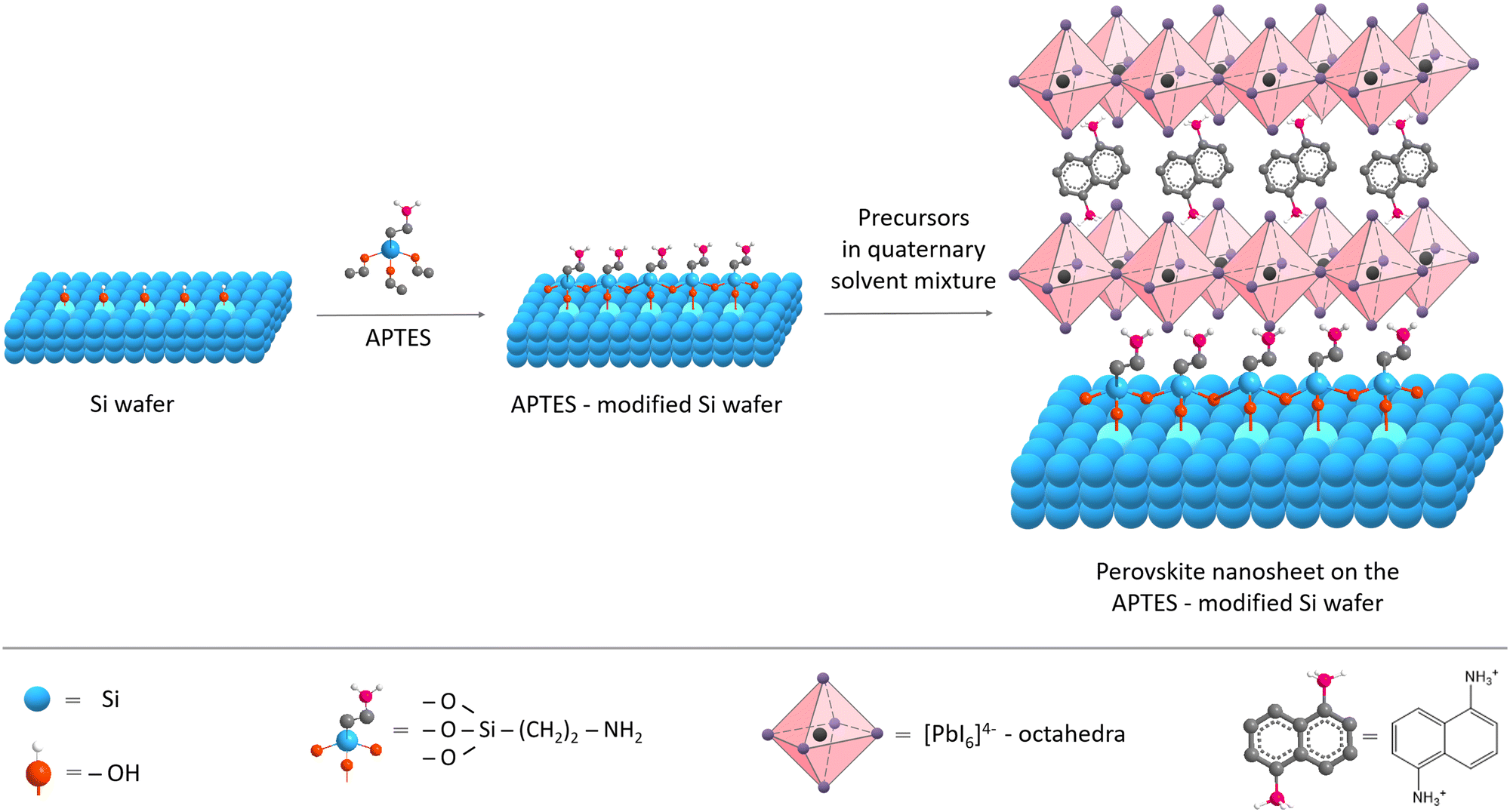 | ||
| Fig. 1 Schematic illustration of the sequential modification and growth of perovskite NSs. | ||
The APTES molecules undergo a condensation reaction with the hydroxyl groups on the substrate (Si wafer, glass) surface. Compared to liquid-phase deposition, vapor deposition treatment provides a higher amine density on the substrate surface and more homogeneous and smoother films of APTES.29
The preparation of perovskite NSs with our bivalent 1,5-diaminonaphthalene ligand was carried out using the solvent evaporation method, first reported by Dou et al.,17 and adjusted in the later works of the same group.14,30,32 For the synthesis of NSs, a quaternary solvent system consisting of dimethylformamide (DMF), chlorobenzene (CB), acetonitrile (AN), and dichlorobenzene (DCB) was chosen. DMF is a suitable solvent for the perovskite systems, whereas CB causes precipitation of the perovskite crystals, and the AN tends to have an intermediate position. The role of AN and DCB, as discussed earlier,17,32 is to moderate the processes of the dissolution and crystallization of the perovskite NSs. Having a lower boiling point, AN evaporates first, reducing the solubility of perovskite and initiating crystallization. DCB has a higher boiling point than other solvents used, and its addition helps to prevent the increase in solution concentration after AN and CB evaporate, which allows a more uniform distribution of NSs on the substrate.
Fig. 2 shows SEM images of the perovskite particles grown using the solvent evaporation approach on the Si wafers with and without APTES modification. The particles grown on the non-modified substrate represent needles of different thicknesses and average lengths of 25 μm (Fig. 2a and c). In contrast, the sheets obtained on the APTES-modified Si wafer are round-shaped with irregular edges and an average diameter of 3 μm (Fig. 2b and d).
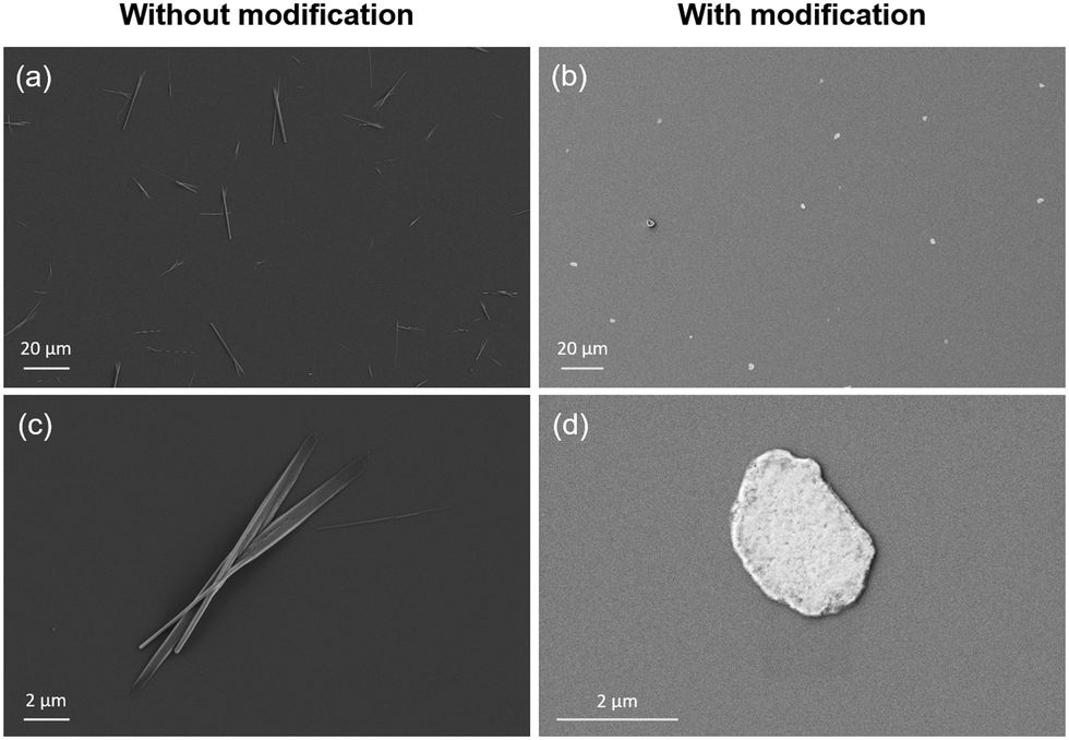 | ||
| Fig. 2 SEM images of perovskite particles and sheets grown on unmodified (a) and (c) and APTES-modified (b) and (d) Si wafer. | ||
Using the approach, we could successfully grow the NSs on different substrates such as Si wafers, SiOx-coated copper TEM grids (see below, Fig. 4b and c), and ITO glass (see below, Fig. 6).
The thickness and morphology of the NSs were imaged using topographic AFM. Fig. 3 demonstrates the variation in NS thicknesses grown at RT on the modified Si substrate. The AFM images reveal round-shaped sheets with almost flat surfaces and an average height of around 40 nm. The thinnest part of the NSs was about 30 nm, related to the approx. 25 perovskite layers of (1,5-DAN)PbI4 (Fig. S1, ESI†).
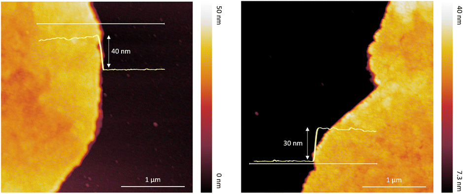 | ||
| Fig. 3 AFM images of (1,5-DAN)PbI4 NSs with different thicknesses grown on Si wafer. | ||
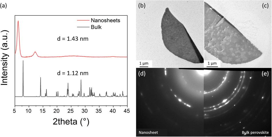 | ||
| Fig. 4 Structure characterization of the obtained NSs. (a) Comparison of GIWAXS pattern from (1,5-DAN)PbI4 NSs and bulk reference (single crystal), (b) and (c) TEM images of the NSs grown on the modified TEM grid, (d) SAED patterns of the NS (displayed in Fig. 4c), and (e) bulk reference. | ||
The temperature of evaporation and concentration of precursors (PbI2 and (1,5-DAN)I2) strongly affect the growth of NSs. Whereas the (1,5-DAN)PbI4 NSs grown at mild conditions (RT) have regular shapes and uniform thickness, the higher temperature (50 °C) produced non-uniform sheets (Fig. S2b, ESI†), indicating inhomogeneous growth due to faster solvent evaporation. The optimal precursor concentration was 5 mM. The higher concentration (10 mM) led to thicker NSs or caused the formation of stacks (Fig. S3c, ESI†). The solution with a concentration of 20 mM reached the solubility limit after adding the CB/AN/DCB mixture. A lower concentration (2.5 mM) gave only small spherical particles (Fig. S3a, ESI†). For the crystal structure determination, grazing incidence wide-angle X-ray scattering (GIWAXS) and electron diffraction in TEM were used. The GIWAXS pattern (Fig. 4a) demonstrates that the NSs give pronounced peaks at 6.2° and 12.3° corresponding to the d spacing of 1.43 nm and indicating highly oriented sheets. The spacing is greater than the one calculated for the bulk form (single crystal) of this material.13 The (1,5-DAN)PbI4 in the bulk form possesses a highly distorted lattice with a Pb–I–Pb bond angle of 150.67° (Fig. S4, ESI†), which is assumed to be relaxed in the NSs, realized probably through the organic cation rearrangement, and changing of the corresponding crystal parameters. This phenomenon has been previously reported for (C4H9NH3)2PbBr4 perovskite sheets.17 We did not observe a sharp peak at 12.7° typical for PbI2 (001) planes, which indicates the absence of a distinct lead iodide phase in the NSs. Additional structure characterization was done by selected area electron diffraction (SAED) using TEM. For that, the (1,5-DAN)PbI4 NSs were grown directly on the APTES-modified SiOx-coated copper grid. Fig. 4b–e shows the TEM images and one-fourth of the SAED pattern of the NSs. SAED pattern (Fig. 4d and e) is represented by concentric rings, indicating the polycrystalline nature of the NSs and showing the similarity between NSs and the bulk phase.
A STEM-EDX analysis was performed to get better insight into the composition of synthesized (1,5-DAN)PbI4 perovskite NSs. The TEM image of NS and elemental mapping images of lead, iodine, carbon and nitrogen are shown in Fig. 5. The elements are all present in the NS, and elemental distribution is uniform throughout almost the whole sheet. The Pb/I ratio is 1:2.4 (Fig. S5, ESI†), which is lower than the expected stoichiometry (1:4), probably because of the volatilization of I-with organic species.33
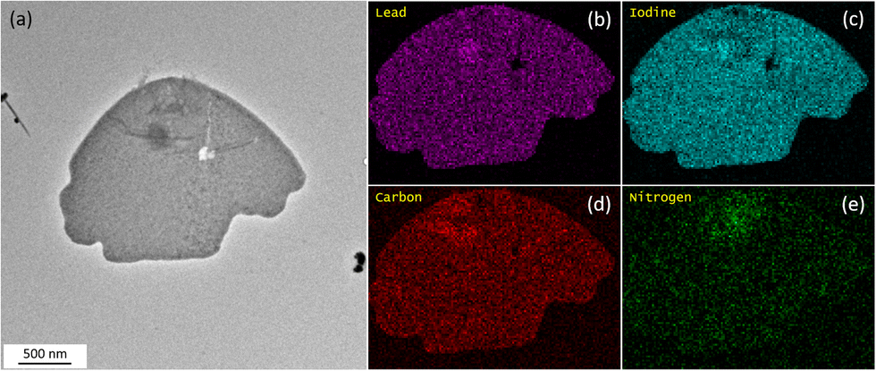 | ||
| Fig. 5 (a) TEM image and (b)–(e) elemental maps calculated from STEM-EDX measurements. The NSs were grown on the modified SiO2-coated copper grid. Fig. S5 (ESI†) shows the corresponding STEM image and EDX spectrum. Note the distortion of the STEM image in comparison to the TEM image caused by the drift during STEM-EDX acquisition. | ||
To get an insight into the material's electronic photoresponse, we used Kelvin-probe force microscopy (KPFM) to study the perovskite NSs under illumination with monochromatic light of 405 nm (Fig. 6 and Fig. S6, ESI†) and 458 nm wavelength (Fig. S7, ESI†). Fig. 6b–f shows a KPFM image on (1,5-DAN)PbI4 NSs grown on the modified ITO substrate. The mean contact potential difference (CPD) measured under illumination (Fig. 6b) dropped by approx. 73 mV compared to the dark CPD (Fig. S6d, ESI†). Due to the band-bending at the surface, the photogenerated charge carriers are redistributed in space, resulting in the changed surface potential.
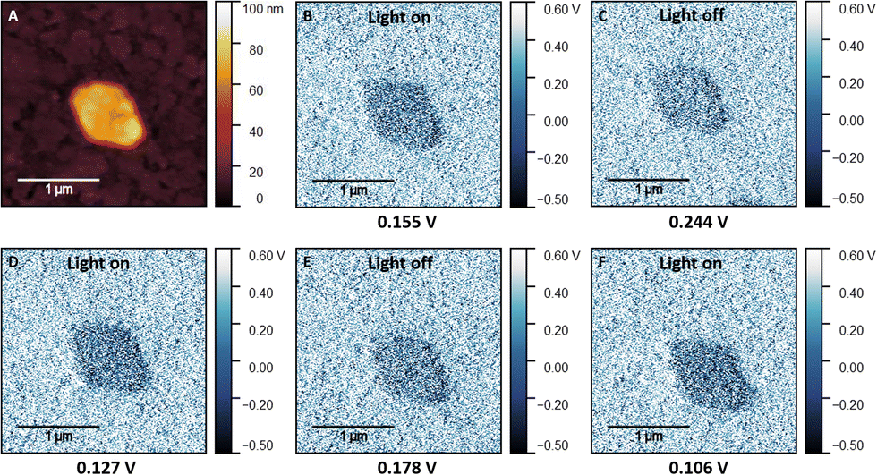 | ||
| Fig. 6 (A) The topography image recorded with the KPFM image. B–F represent the KPFM images during 405 nm illumination (B), (D), and (E), and 50 minutes after the illumination (C) and (E). Average CPD value on the particle is displayed under each image. | ||
After the measurement under illumination, the laser was turned off, and dark measurement was done 50 min later (Fig. 6c). No changes in the morphology of the NSs during the KPFM experiment were observed (Fig. S6, ESI†). Subsequent measurements under illumination with a 458 nm laser (Fig. S7e, ESI†) revealed no detectable response, with the difference between the initial state and during the illumination was approximately 8 mV, below the detection limit of our set-up. The following measurement again under 405 nm illumination (Fig. 6d) showed the more negative CPD, with the difference prior to the second 405 nm illumination and during the second 405 nm illumination was approximately 0.12 V, indicating that the photogeneration process was repeatable and 405 nm illumination served more effective for such purpose. After the following dark measurement (Fig. 6e) the contrast between sheets and substrate became weaker compared to the illuminated state, with corresponding growth of the CPD to the intermediate value that was approximately 60 mV lower than the initial value before the illumination. The third 405 nm illumination resulted in the lowest CPD value which was 0.021 V lower than the second and 0.049 V lower than the CPD value during the first illumination. It may indicate that the generated charge carriers during the illumination period are trapped within the perovskite structure, making the initial state before the illumination not reachable after more than two illumination cycles.
The surface photovoltage (SPV), defined as the illumination-induced change in surface potential, equals the difference between CPDlight and CPDdark. The sign of the SPV determines the polarity of the sample surface.34,35 For p-type semiconductors, a negative SPV arises under illumination. SPV is positive for the n-type semiconductor. In our experiment, negative SPV values were observed throughout the whole sheets, suggesting the p-type nature of the material. In general, such change in the SPV can be attributed to the increased number of photogenerated charge carriers. This effect, observed by KPFM, allows us to assume enhanced charge carrier concentration and thus conductivity of NSs under illumination.
Conclusions
In summary, we have synthesized for the first time perovskite NSs containing the bivalent conjugated organic cations from 1,5-diaminonaphthalene. In addition, we demonstrated that a surface-assisted approach can be successfully used to take control of the NSs’ growth and morphology. Anchoring silane molecules enhanced the contact between the perovskite material and substrate, resulting in NSs that were several micrometers in lateral size and a few tens of nm thick. Structural investigations showed that the NSs undergo structural relaxation, keeping the crystal parameters close to the bulk phase. KPFM revealed the generation of charge carriers under illumination and suggests a p-type nature of the investigated material. Considering the simplicity and versatility of the modification process, we can anticipate that these NSs, together with a surface modification approach, offer good potential for future applications in photodetectors.Author contributions
A. M., B. V. and Q. A. B. conceived and planned the experiments. B. V. and Q. A. B. supervised the work. A. M. synthesized the nanosheets and prepared the samples with the help of K. Z. K. R. performed the surface modification. P. F. performed the SEM and TEM measurements, and D. P. performed STEM and EDX measurements together with EDX evaluation. A. M. performed the AFM measurements. E. B. performed the GIWAXS measurements. D. S. performed the KPFM measurements with the supervision of I. M. H. A. M. wrote the manuscript. All authors have discussed the results and commented on the final manuscript.Conflicts of interest
There are no conflicts to declare.Acknowledgements
The Deutsche Forschungsgemeinschaft (DFG) is gratefully acknowledged for funding projects CRC 1415 (A. M., K. Z. and B. V.), 456180046 (D. S.), and 49620170 (BE 7737/2-1) (K. R. and Q. A. B.). The authors thank Hannes Kettner for the help with GIWAXS measurements.References
- M. Chhowalla, H. S. Shin, G. Eda, L. J. Li, K. P. Loh and H. Zhang, Nat. Chem., 2013, 5, 263–275 CrossRef PubMed.
- W. Lei, V. N. Mochalin, D. Liu, S. Qin, Y. Gogotsi and Y. Chen, Nat. Commun., 2015, 6, 1–8 Search PubMed.
- S. Ithurria and B. Dubertret, J. Am. Chem. Soc., 2008, 130, 16504–16505 CrossRef CAS PubMed.
- K. S. Novoselov, A. K. Geim, S. V. Morozov, D. Jiang, Y. Zhang, S. V. Dubonos, I. V. Grigorieva and A. A. Firsov, Science, 2004, 306, 666–669 CrossRef CAS PubMed.
- L. Zhang, C. Sun, T. He, Y. Jiang, J. Wei, Y. Huang and M. Yuan, Light: Sci. Appl., 2021, 10, 1–26 CrossRef PubMed.
- S. Kumar, J. Jagielski, N. Kallikounis, Y. H. Kim, C. Wolf, F. Jenny, T. Tian, C. J. Hofer, Y. C. Chiu, W. J. Stark, T. W. Lee and C. J. Shih, Nano Lett., 2017, 17, 5277–5284 CrossRef CAS.
- C. Ma, C. Leng, Y. Ji, X. Wei, K. Sun, L. Tang, J. Yang, W. Luo, C. Li, Y. Deng, S. Feng, J. Shen, S. Lu, C. Du and H. Shi, Nanoscale, 2016, 8, 18309–18314 RSC.
- A. H. Proppe, A. Johnston, S. Teale, A. Mahata, R. Quintero-Bermudez, E. H. Jung, L. Grater, T. Cui, T. Filleter, C. Y. Kim, S. O. Kelley, F. De Angelis and E. H. Sargent, Nat. Commun., 2021, 12, 1–9 CrossRef.
- Y. Zhang, Y. Liu, Z. Xu, H. Ye, Q. Li, M. Hu, Z. Yang and S. Liu, J. Mater. Chem. C, 2019, 7, 1584–1591 RSC.
- I. H. Park, K. C. Kwon, Z. Zhu, X. Wu, R. Li, Q. H. Xu and K. P. Loh, J. Am. Chem. Soc., 2020, 142, 18592–18598 CrossRef CAS PubMed.
- W. Zhao, R. Zhang, S. Wang, D. Zheng, Q. Kong, J. Liu, J. Li, J. Guo, S. Yang and K. Han, J. Phys. Chem. C, 2021, 125, 23889–23894 CrossRef CAS.
- J. Yang, T. He, M. Li, G. Li, H. Liu, J. Xu, M. Zhang, W. Zuo, R. Qin, M. H. Aldamasy, M. Yuan, Z. Li, M. Malekshahi Byranvand, M. Saliba and A. Abate, ACS Energy Lett., 2022, 7, 4451–4458 CrossRef CAS.
- A. Mitrofanov, Y. Berencén, E. Sadrollahi, R. Boldt, D. Bodesheim, H. Weiske, F. Paulus, J. Geck, G. Cuniberti, A. Kuc and B. Voit, J. Mater. Chem. C, 2023, 11, 5024–5031 RSC.
- Y. Gao, E. Shi, S. Deng, S. B. Shiring, J. M. Snaider, C. Liang, B. Yuan, R. Song, S. M. Janke, A. Liebman-Peláez, P. Yoo, M. Zeller, B. W. Boudouris, P. Liao, C. Zhu, V. Blum, Y. Yu, B. M. Savoie, L. Huang and L. Dou, Nat. Chem., 2019, 11, 1151–1157 CrossRef CAS.
- J. V. Passarelli, D. J. Fairfield, N. A. Sather, M. P. Hendricks, H. Sai, C. L. Stern and S. I. Stupp, J. Am. Chem. Soc., 2018, 140, 7313–7323 CrossRef CAS PubMed.
- J. Rodríguez-Romero, B. C. Hames, I. Mora-Seró and E. M. Barea, ACS Energy Lett., 2017, 2, 1969–1970 CrossRef.
- L. Dou, A. B. Wong, Y. Yu, M. Lai, N. Kornienko, S. W. Eaton, A. Fu, C. G. Bischak, J. Ma, T. Ding, N. S. Ginsberg, L.-W. Wang, A. P. Alivisatos and P. Yang, Science, 2015, 349, 1518–1521 CrossRef CAS PubMed.
- O. Yaffe, A. Chernikov, Z. M. Norman, Y. Zhong, A. Velauthapillai, A. Van Der Zande, J. S. Owen and T. F. Heinz, Phys. Rev. B: Condens. Matter Mater. Phys., 2015, 92, 045414 CrossRef.
- A. Kostopoulou, I. Konidakis and E. Stratakis, Nanophotonics, 2023, 12, 1643–1710 CrossRef CAS.
- A. G. Ricciardulli, S. Yang, J. H. Smet and M. Saliba, Nat. Mater., 2021, 20, 1325–1336 CrossRef CAS.
- S. Yang, W. Niu, A.-L. Wang, Z. Fan, B. Chen, C. Tan, Q. Lu and H. Zhang, Angew. Chem., Int. Ed., 2017, 129, 4316–4319 CrossRef.
- X. Fu, S. Jiao, Y. Jiang, L. Li, X. Wang, C. Zhu, C. Ma, H. Zhao, Z. Xu, Y. Liu, W. Huang, W. Zheng, P. Fan, F. Jiang, D. Zhang, X. Zhu, X. Wang and A. Pan, ACS Appl. Mater. Interfaces, 2020, 12, 2884–2891 CrossRef CAS.
- K. Leng, I. Abdelwahab, I. Verzhbitskiy, M. Telychko, L. Chu, W. Fu, X. Chi, N. Guo, Z. Chen, Z. Chen, C. Zhang, Q. H. Xu, J. Lu, M. Chhowalla, G. Eda and K. P. Loh, Nat. Mater., 2018, 17, 908–914 CrossRef CAS PubMed.
- J. Lu, L. Jiang, W. Li, F. Li, N. K. Pai, A. D. Scully, C. M. Tsai, U. Bach, A. N. Simonov, Y. B. Cheng and L. Spiccia, Adv. Energy Mater., 2017, 7, 1700444 CrossRef.
- Y. Ogomi, A. Morita, S. Tsukamoto, T. Saitho, Q. Shen, T. Toyoda, K. Yoshino, S. S. Pandey, T. Ma and S. Hayase, J. Phys. Chem. C, 2014, 118, 16651–16659 CrossRef CAS.
- L. Liu, A. Mei, T. Liu, P. Jiang, Y. Sheng, L. Zhang and H. Han, J. Am. Chem. Soc., 2015, 137, 1790–1793 CrossRef CAS PubMed.
- W. Wei, Y. Zhang, Q. Xu, H. Wei, Y. Fang, Q. Wang, Y. Deng, T. Li, A. Gruverman, L. Cao and J. Huang, Nat. Photonics, 2017, 11, 315–321 CrossRef CAS.
- X. Li, J. M. Hoffman and M. G. Kanatzidis, Chem. Rev., 2021, 121, 2230–2291 CrossRef CAS.
- S. Xiang, G. Xing, W. Xue, C. Lu and J. M. Lin, Analyst, 2012, 137, 1669–1673 RSC.
- Akriti, E. Shi, S. B. Shiring, J. Yang, C. L. Atencio-Martinez, B. Yuan, X. Hu, Y. Gao, B. P. Finkenauer, A. J. Pistone, Y. Yu, P. Liao, B. M. Savoie and L. Dou, Nat. Nanotechnol., 2021, 16, 584–591 CrossRef CAS.
- G. Yang, C. Wang, H. Lei, X. Zheng, P. Qin, L. Xiong, X. Zhao, Y. Yan and G. Fang, J. Mater. Chem. A, 2017, 5, 1658–1666 RSC.
- E. Shi, B. Yuan, S. B. Shiring, Y. Gao, Akriti, Y. Guo, C. Su, M. Lai, P. Yang, J. Kong, B. M. Savoie, Y. Yu and L. Dou, Nature, 2020, 580, 614–620 CrossRef CAS.
- Y. Zhou, H. Sternlicht and N. P. Padture, Joule, 2019, 3, 641–661 CrossRef CAS.
- E. Choi, Y. Zhang, A. M. Soufiani, M. Lee, R. F. Webster, M. E. Pollard, P. J. Reece, W. Lee, J. Seidel, J. Lim, J. H. Yun and J. S. Yun, npj 2D Mater. Appl., 2022, 6, 43 CrossRef CAS.
- R. Chen, F. Fan, T. Dittrich and C. Li, Chem. Soc. Rev., 2018, 47, 8238–8262 RSC.
Footnote |
| † Electronic supplementary information (ESI) available: SEM images of NSs grown at different temperatures and initial precursor concentrations; the structure of layered perovskite; degree of structure distortion; STEM image with EDX spectrum; additional KPFM images. See DOI: https://doi.org/10.1039/d3tc04080a |
| This journal is © The Royal Society of Chemistry 2024 |