DOI:
10.1039/D3TC03805J
(Paper)
J. Mater. Chem. C, 2024,
12, 1888-1896
In2Si2S3X3 (X = S, Se, Te) Janus monolayers: from magnetic element-free spin-Hall transistor to sustainable energy generation†
Received
18th October 2023
, Accepted 2nd January 2024
First published on 2nd January 2024
Abstract
Conventional spintronics uses ferromagnets for spin generation and detection; however, recent experiments have demonstrated highly efficient ferromagnet-free spin-Hall transistors. In this work, we propose a novel multiatomic direct band gap Janus In2Si2S3Te3 monolayer as a channel semiconductor that exhibits a finite spin-Hall conductivity with high charge carrier mobility of 2772 cm2 V−1 s−1 at room temperature. In this model device, a pure spin current can be generated from the charge current using the spin-Hall effect whereas the inverse spin-Hall effect can be used to generate a Hall voltage. Further, this monolayer is predicted to possess a large out-of-plane piezoelectric coefficient of 160 pm V−1 originating from crystal asymmetry and low elastic stiffness. A three-fold enhancement in solar to hydrogen efficiency is obtained for the Janus In2Si2S3Se3 monolayer (∼7.32%) compared to its pristine In2Si2S6 monolayer (∼2.44%). Moreover, this work provides detailed theoretical insights into the emergent electronic and piezoelectric properties of multi-atomic In2Si2S3X3 (X = S, Se, Te) monolayers. Experimental synthesis of multi-atomic CuInP2S6 nanosheets paves the way for the exploration of the proposed semiconductors in spintronics, piezotronics, and water splitting.
Introduction
Spintronics, short for ‘spin transport electronics’, is an emerging field in electronics that exploits an electron's intrinsic spin degrees of freedom, in addition to its fundamental charge. Spintronics has the potential to revolutionize the field of electronics offering several key advantages over traditional electronics in terms of energy efficiency, increased data storage density, and faster data processing. However, generation, manipulation, and detection of pure spin current are the key challenges for spin-based electronics. Kramer's degeneracy theorem1 depicts double spin-degeneracy under both spatial inversion and time reversal symmetries as illustrated below;
Under time reversal symmetry (ℑ), the relationship between energy eigenvalues of spin +1/2 and −1/2 is given by;
| | | ℑ: ε↑(k) = ε↓(−k) and ε↓(k) = ε↑(−k) | (1) |
and under inversion symmetry (I);
| | | I: ε↑(k) = ε↑(−k) and ε↓(k) = ε↓(−k) | (2) |
Combining both time reversal and inversion symmetries, a double spin degeneracy is obtained in the energy dispersion within the whole Brillouin zone (BZ).
2However, for the generation of spin current, one of the above symmetries needs to be broken to lift the spin degeneracy by spin–orbit coupling (SOC).
The Rashba SOC in a system arises from the structure's inversion asymmetry.3 Recently, there has been considerable interest in discovering new semiconductors with strong SOC. The ideal Rashba semiconductor needs to have an internal out-of-plane electric field (Ez) and significant efforts have been made to break the out-of-plane mirror symmetry to induce Ez such as in Janus structures.
The effective Hamiltonian of the Rashba model can be represented by;
| |  | (4) |
where
m*,
αR,
σ,
k represent effective mass, Rashba constant, Pauli matrix, and electron wave vector, respectively. The energy dispersions obtained from the Hamiltonian presented in
eqn (4) are given by
| |  | (5) |
where the Rashba constant
αR represents the strength of the SOC.
Eqn (5) indicates that the Rashba effect splits the degenerate bands into two distinct energy states in the momentum space. The spin precession in Rashba semiconductors can be precisely manipulated using an external vertical electric field.
Analogous to the Hall effect, a pure spin current can be generated perpendicular to the applied electric field in a system having strong SOC, giving rise to a spin-Hall effect (SHE).4,5 And with the reverse of the same mechanism, termed as inverse spin Hall effect (ISHE), a spin current can induce a transverse charge imbalance and a measurable voltage.5 According to the Onsager symmetry relations,6 these ‘direct’ and ‘reverse’ effects are mathematically equivalent. SHE can arise in a system from topological band structure referred to as intrinsic, or from asymmetry in electron scattering for spin-up/down referred to as extrinsic. Both mechanisms originate from the SOC. These two effects, SHE and ISHE, have been experimentally realized in different systems and, if combined, a reciprocal conversion between spin and charge currents can be achieved which is essential in harmonizing spintronics with conventional electronics.7
Modern energy research focuses mostly on sustainable energy generation from renewable resources such as generating electricity from waste heat, mechanical energy, and solar energy. In conventional electronics, external gate voltage is used. However, recent experiments have demonstrated the usage of piezoelectric semiconductors for self-powered devices.8–10 Piezoelectric materials that have intrinsic inversion asymmetry in the crystal structure can generate electric charges when subjected to mechanical stress and vice versa. 2D materials often exhibit higher piezoelectric coefficients compared to bulk materials which implies that they can generate larger electric charges in response to a given mechanical deformation, making them more sensitive and responsive for sensor applications. Recently, Janus structures have been gaining a lot of interest and are considered an ideal platform for experimentalists to induce many interesting properties that are absent in the parent pristine structure.11–13 In Janus structures, the main interest is in the out-of-plane electric field originating from broken mirror symmetry along the z-direction and, hence, additional properties such as out-of-plane piezoelectricity can be induced.14 The atomic thick 2D piezoelectric materials can be easily integrated into micro and nanoscale devices, enabling miniaturization of sensors and actuators and more importantly in self-powered electronic devices demonstrated experimentally.15,16 Besides the conversion of mechanical energy, semiconductors have been constantly utilizing solar energy for the production of hydrogen and oxygen from water termed as hydrogen evolution reaction (HER) and oxygen evolution reaction (OER). There are various intermediate steps involved in the decomposition of H2O molecule having uneven energy steps. The term theoretical overpotential (η) in water splitting is used to describe the maximum voltage that needs to be applied which can thermodynamically favor all the intermediate redox reaction processes.
In this work, Janus structures are designed from the parent In2Si2S6 monolayer, and their stability and materials properties, such as electronic and piezoelectric originating from broken mirror symmetry along the z-direction, are evaluated using density functional theory (DFT).
Results and discussions
Geometry and associated symmetry of 2D structures
A triatomic unit cell composed of In, Si and S atoms in the ratio 1![[thin space (1/6-em)]](https://www.rsc.org/images/entities/char_2009.gif) :1:3 is constructed as a parent 2D material and its Janus structures are designed by replacing top S-atom with Se and Te-atoms. The crystallographic information of all the monolayers is provided in Table 1. The geometrical top and side views are plotted in Fig. 1. The order of the group that represents the number of symmetry operations under which the crystal structure remains invariant gets reduced to half in Janus structures. The phonon dispersion plotted in Fig. S1 (ESI†) along with ab initio molecular dynamics simulation confirm their thermodynamical stability.
:1:3 is constructed as a parent 2D material and its Janus structures are designed by replacing top S-atom with Se and Te-atoms. The crystallographic information of all the monolayers is provided in Table 1. The geometrical top and side views are plotted in Fig. 1. The order of the group that represents the number of symmetry operations under which the crystal structure remains invariant gets reduced to half in Janus structures. The phonon dispersion plotted in Fig. S1 (ESI†) along with ab initio molecular dynamics simulation confirm their thermodynamical stability.
Table 1 Crystallographic information of pristine and Janus monolayers
| Monolayers |
Space group number |
System |
Schoenflies symbol |
International symbol |
Order of the group |
| In2Si2S6 |
162 |
Trigonal |
D3d1 |
P![[3 with combining macron]](https://www.rsc.org/images/entities/char_0033_0304.gif) 1m 1m |
12 |
| In2Si2S3Se3 |
157 |
Trigonal |
C3v2 |
P31m |
6 |
| In2Si2S3Te3 |
157 |
Trigonal |
C3v2 |
P31m |
6 |
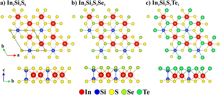 |
| | Fig. 1 Top and side geometrical view of 2D monolayers (a) In2Si2S6, (b) Janus In2Si2S3Se3 and (c) Janus In2Si2S3Te3. | |
Electronic properties with and without relativistic effect
The electronic band structures of all the monolayers evaluated using the density functional theory (DFT) are plotted in Fig. 2. In2Si2S6 and In2Si2S3Se3 monolayers are found to be indirect band gap semiconductors whereas In2Si2S3Te3 is a direct band gap semiconductor. The conduction band minima (CBM) of all these monolayers are located at the Γ-point of the hexagonal Brillouin zone, irrespective of the valence band maxima (VBM). The atomic composition of CBM can be found from the atom-projected density of states (PDOS) plot in Fig. S2 (ESI†). The CBM is mainly composed of S-atom in the parent monolayer whereas equally contributed by chalcogens (S/Se/Te) in Janus structures. The band gaps of monolayers calculated using different functionals are provided in Table 2.
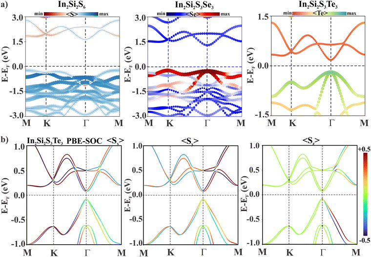 |
| | Fig. 2 (a) DFT obtained electronic band structure of 2D monolayers using GGA-PBE and (b) spin projected band structure of Janus In2Si2S3Te3. | |
Table 2 Calculated band gap using different functional and Rashba constant
| Monolayers |
Band gap (eV) |
Semiconductor |
Rashba constant (eV Å) |
| GGA-PBE |
HSE |
| In2Si2S6 |
1.86 |
2.76 |
Indirect |
— |
| In2Si2S3Se3 |
1.51 |
2.38 |
Indirect |
— |
| In2Si2S3Te3 |
0.36 |
1 |
Direct |
0.73 |
Since Janus In2Si2S3Te3 is composed of heavy Te-atom, the relativistic effect is incorporated in the band structure calculation and plotted in Fig. 2(b). The effect of spin–orbit coupling can be depicted from the band structure plot. The band gap is reduced and a Rashba-type spin-splitting occurs at the CBM. The strength of spin–orbit coupling known as the Rashba constant (α) along the Γ→M direction can be calculated from the band structure using eqn (6).
| |  | (6) |
where
ER is the energy difference between the CBM and the band crossing at the
Γ-point and
kR is the momentum offset.
17–19 The characteristic parameters quantifying the strength of the Rashba splitting along the Γ→M direction are; the momentum offset
kR = 0.0136 Å and the Rashba energy
ER = 0.005 eV and the Rashba constant is 0.73 eV Å which is comparable to WSeTe monolayer (0.92 eV Å) and buckled ZnTe (1.06 eV Å). Janus In
2Si
2S
3Te
3 shows that the Rashba splitting at the CBM is due to the built-in out-of-plane electric field
Ez coupled with p
z orbitals
i.e.; 〈p
z|
Ez|p
z〉 ≠ 0.
20 The CBM is composed of ∼25% p
z orbital whereas VBM is composed of ∼5%. The Te_p
z orbital projected band structure is plotted in Fig. S3 in ESI.
† There are two distinctive features of Rashba spin splitting; momentum dependent energy band splitting and in-plane spin splitting. The spin projected band dispersion in
Fig. 2 shows that the in-plane spin components S
x and S
y are dominating in CBM. For a comparative analysis, the energy dispersion and spin projection of eigenstates obtained from Rashba Hamiltonian as in
eqn (4) are plotted in
Fig. 3(a).
21 The constant energy Fermi surface indicates the energy dispersions form concentric circles whereas the inner and outer dispersions show a momentum dependent spin orientation. Since the Rashba type spin splitting occurs at conduction band, for a systematic comparison, the DFT obtained spin projections on two lowest conduction bands are plotted in
Fig. 3(b) which matches exactly with that of obtained using analytical model. The spin-projected Fermi surface indicates that the spin directions of the inner and outer branches are opposite which form a characteristic spin chiral structure. The spin-projected band structures for In
2Si
2S
6 and Janus In
2Si
2S
3Se
3 are plotted in Fig. S4 (ESI
†) where Rashba splitting is negligible.
 |
| | Fig. 3 (a) Constant energy Fermi surface and spin projected Rashba bands obtained from Rashba Hamiltonian as in eqn (4), (b) DFT calculated spin texture of two lowest conduction bands of Janus In2Si2S3Te3 and spin-projected constant energy contour plots of spin texture calculated in the kx – ky plane centred at the Γ-point. | |
Ferromagnet-free electric control spin-Hall transistor
In conventional spintronic devices, ferromagnetic materials are used as source and drain to generate and detect spin. Nevertheless, 100% spin current generation with efficient spin injection source to channel and detect from channel to drain limits the efficiency of the device. To overcome such limitations imposed by the device architecture, a recent experiment by Choi et al.22 demonstrated an energy-efficient ferromagnet-free spin-Hall transistor combining spin-Hall effect (SHE) and inverse spin-Hall effect (ISHE). A schematic of an all-electric spin-Hall transistor (SHT) is presented in Fig. 4. Only a single material exhibiting SOC is used in the proposed device and hence free from any magnetic element.
 |
| | Fig. 4 (a) Schematic of a spin-Hall transistor; R represents different regions, SHE and ISHE stands for spin-Hall effect and inverse spin-Hall effect, (b) calculated spin-Hall conductivity (SHC), (c) SHC projected band structure and (d) k-point resolved SHC. | |
The device has three regions. In region R-I, the spin-polarized current (Is) is generated from the charge current (Ic) from SHE given by;
where
σ is the spin polarization direction and
Is/
Ic is the flow of spin/charge current. The spin-polarized electrons are injected into R-II where the spin precession rate is controlled by using a vertical electric field, also called the gate voltage (
Vg). The gate-modulated spins are injected into region R-III where the spin-current is converted back to the charge current given by
eqn (8)23 and, thus, a Hall voltage is generated in R-III.
Eqn (7) and (8) resembles that of Lorentz force. The Hall voltage in R-III oscillates with the
z-component of the injected spin, which can be controlled by the gate voltage. The proposed device relies on these three processes, SHE, modulation of spin precession by gate voltage, and ISHE for pure spin current generation, manipulation, and detection. The spin-Hall conductivity (SHC) which measures the SHE is calculated for Janus In
2Si
2S
3Te
3 and plotted in
Fig. 4(b) and (c) which shows finite SHE at the band edges and mostly localized at the Brillouin zone center. Since Janus In
2Si
2S
3Te
3 is a semiconductor, the SHC value is of the order ∼10
2 compared to that of heavy metals such as Pt (∼10
3)
24 and comparable to other semiconductors such as GeSe, GeTe, SnSe, SnTe, and Janus MoSSe (∼10
2).
25,26 The SHC curve for the semiconductors possesses certain similarities near the band edges, as the energy increases, the SHC drops to zero at the VBM and an obvious peak emerges at the CBM. Similar distinguishing features of SHC have been observed on other semiconductor materials as well.
26
Further, the charge carrier mobility of Janus In2Si2S3Te3 is calculated using the Boltzmann transport equation (BTE) method beyond effective mass approximation. The electron charge carrier mobility is found to be 2772 cm2 V−1 s−1 at room temperature which is much higher than SnGe (855 cm2 V−1 s−1)27 and InP (1022.7 cm2 V−1 s−1)28 within the same formalism.
Piezoelectric properties
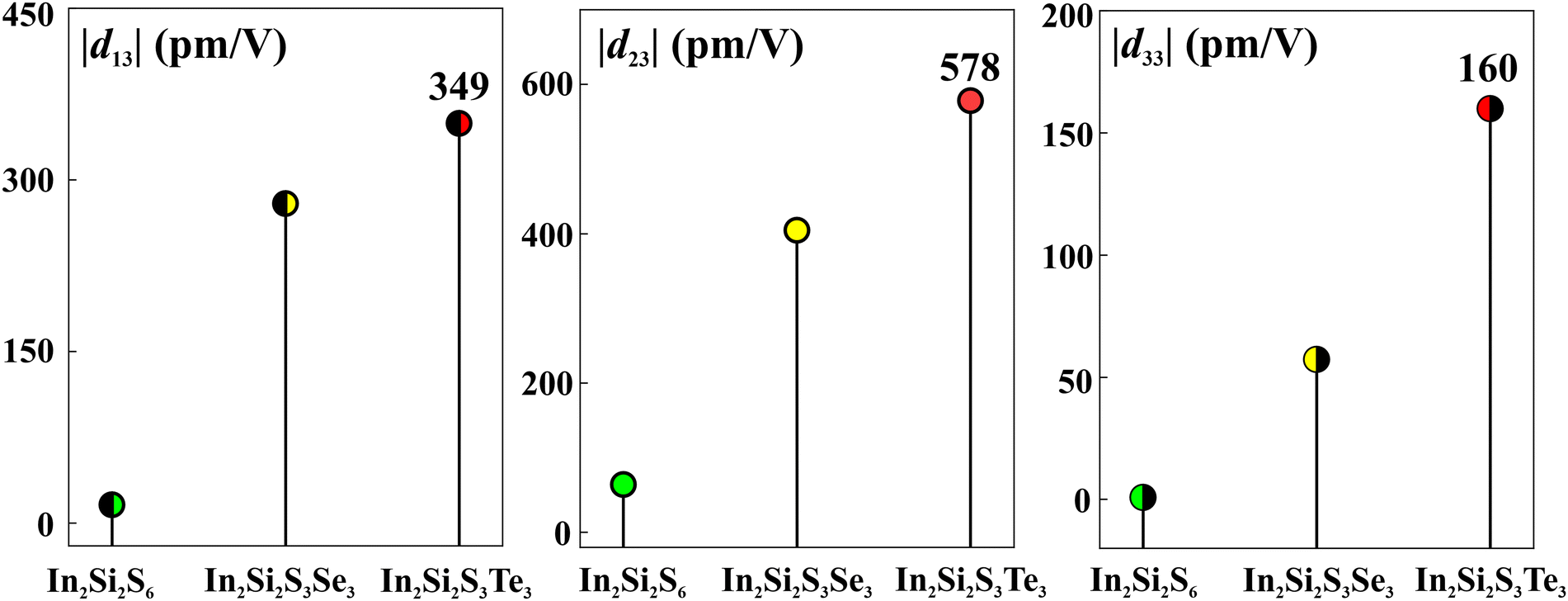
Piezoelectric property in 2D semiconductors is one of the most prominent features of non-centrosymmetric crystal structure. Owing to its unique atomic configuration and low elastic stiffness (see Table S1, ESI†), all the monolayers under study exhibit excellent piezoelectric coefficients.
Unlike MoS2, the S-atom at the top and bottom sides are not mapped by vertical mirror symmetry operation in pristine In2Si2S6 monolayer; hence, it exhibits significant out-of-plane (d13,d23,d33) coefficients which get enhanced in Janus structures29 as depicted in Fig. 5. The first index 1/2/3 represents the direction of induced piezo-polarization and the second index represents the direction of applied stress/strain. A distinctive existence of non-zero piezoelectric component of d13 and d23 in pristine In2Si2S6 indicates presence of electrical polarity in the system which is true since these monolayers are ferroelectric.30–32 These piezoelectric components, particularly d33, is very important in designing various devices. Such high out-of-plane piezoelectric coefficients in Janus In2Si2S3Te3 monolayer holds immense potential in different applications such as strain sensor, actuators, MEMS devices, and more importantly self-powered electronic device. The out-of-plane coefficients of Janus In2Si2S3Te3 in this work are comparable to, if not surpass that of other monolayers; Janus Bi2Se2S (173.14 pm V−1),33 Janus ZrSe2S (68.72 pm V−1),34 Janus MoSSe (4.26 pm V−1),29 CdS (56 pm V−1),35 and Janus MoSTe/WSTe multilayer (10.57/9.28 pm V−1).14 The reliability of the robust formalism used to calculate piezoelectric coefficients can be confirmed from earlier work by Mohanta and De Sarkar29 where prediction of out-of-plane piezoelectric coefficient d33 of MoSSe/BP van der Waals heterostructure (vdWH) (∼15 pm V−1) is in excellent agreement with the experimental report of 17.5 pm V−1 in a similar vdWH system In2Se3/MoS2.36 Nevertheless, recent experiments30–32 on a similar crystal structure nanosheet CuInP2S6 for ferroelectric Schottky diodes provide an essential platform to explore the proposed semiconductors in piezoelectric nanodevices.
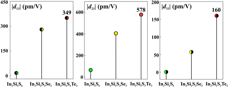 |
| | Fig. 5 Calculated out-of-plane piezoelectric coefficients of pristine and Janus structures. | |
Atomistic thermodynamic framework for hydrogen evolution and oxygen evolution
Further, 2D semiconductors having a band gap larger than 1.23 eV can be used as excellent photocatalysts utilizing solar energy to convert water into hydrogen and oxygen.| | | Oxidation reaction: 2H2O + 4h+ → O2 + 4H+ | (9) |
| | | Reduction reaction: 2H+ + 2e− → H2 | (10) |
The photoexcited charge carriers in semiconductors participate in the oxidation and reduction process of water as presented in eqn (9) and (10). The out-of-plane built-in polarization originating from structural asymmetry is expected to restrain the carrier recombination and accelerate the hydrogen evolution reaction (HER) and oxygen evolution reaction (OER) in Janus In2Si2S3Se3 structure compared to pristine monolayer. The position of band edges with respect to standard water redox potentials are plotted in Fig. 6(a). Since Janus structures have two faces, HER and OER can occur on both surfaces. The Gibbs free energy profile for HER and OER plotted in Fig. 6 indicates HER is favourable at the S-side whereas OER is favourable at the Se-side. The theoretical overpotential required to make each intermediate step for the OER is calculated to be 1.14 V and 1.72 V for Se-side and S-side respectively. Thus, Janus In2Si2S3Se3 can be used as an efficient bifunctional catalyst for water splitting. The Gibbs free energy profile of the pristine monolayer is plotted in Fig. S5 (ESI†). Various equations and DFT-obtained values used for determining free energies are provided in the ESI.†
 |
| | Fig. 6 (a) Position of band edges of pristine In2Si2S6 and Janus In2Si2S3Se3 with respect to vacuum; the redox potential of HER and OER are indicated by a dashed horizontal line at zero pH, (b)–(d) Gibbs free energy profile of HER and OER on both sides of the Janus In2Si2S3Se3 monolayer. | |
Further, the solar to hydrogen (STH) efficiency (ηSTH) of both In2Si2S6 and In2Si2S3Se3 monolayers are evaluated using a method proposed by Yang et al.37 The STH efficiency is defined as the product of the efficiency of light absorption (ηabs) and carrier utilization (ηcu).
The efficiency of light absorption is defined as:
| |  | (12) |
where
P(ℏ
ω) are the AM1.5G solar energy flux at the photon energy hω and
Eg is the direct band gap of the photocatalyst (
EHSEg). The denominator represents the total power density of the reference sunlight spectrum (AM1.5G) and the numerator gives the light power density absorbed by the photocatalyst.
The efficiency of carrier utilization (ηcu) is defined as:
| | 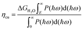 | (13) |
where Δ
GH2O is the free energy of water splitting (1.23 eV) and the rest of the numerator represents the effective photocurrent density. Here,
E represents the photon energy that can be utilized in the process of water splitting.
38–40 The calculated STH efficiency for Janus structure 7.32% is three times larger than of the pristine monolayer owing to a decrease in the band gap and the built-in electric field which is comparable to recent experiments; 13.8% using earth-abundant electrolyser
41 and 9.2% using InGaN.
42 Different parameters used for calculating η
STH is listed in
Table 3. For economical production of hydrogen from water splitting the STH efficiency of the material needs to be greater than 10%, nevertheless this work demonstrates three-fold enhancement of STH
via structural engineering.
Table 3 Light absorption efficiency of semiconductor, carrier utilization, and solar to hydrogen efficiency of monolayers
| Monolayers |
η
abs (%) |
η
cu (%) |
η
STH (%) |
| In2Si2S6 |
14.1 |
17.34 |
2.44 |
| In2Si2S3Se3 |
24.4 |
30.01 |
7.32 |
Conclusions
In summary, we propose a new In2Si2S6 monolayer and its Janus structures that have a similar crystal structure to the recently synthesized CuInP2S6 nanosheets. Using first-principles calculations, we systematically investigate different material properties of these multi-atomic semiconductors. Compared to the pristine In2Si2S6 monolayer, many emergent properties such as the Rashba effect and the giant out-of-plane piezoelectricity are discovered via structural engineering. A detailed theoretical analysis is provided that sheds light on the origin of these properties. Particularly, a finite spin Hall conductivity together with high charge carrier mobility of 2772 cm2 V−1 s−1 in the Janus In2Si2S3Te3 monolayer is proposed for an all-electric control ferromagnet-free spin-Hall transistor where spin-Hall and inverse-spin-Hall effects can be used to generate and detect pure spin current. A large out-of-plane piezoelectric coefficient is found in pristine as well as in Janus monolayers owing to their unique non-centrosymmetric crystal structure which holds immense potential in piezotronics. Further, the DFT results show a threefold enhancement in solar-to-hydrogen conversion efficiency in Janus In2Si2S3Se3 compared to the pristine material. Thus, this work opens a new avenue for application in ferromagnet-free spintronics, piezotronics, and photocatalysis.
Computational details
All calculations are performed using the density functional theory implemented in the VASP code.43,44 The projector-augmented wave (PAW) method is used to describe ion-electron interaction.45 The generalized gradient approximation (GGA) due to Perdew–Burke–Ernzerhof (PBE) is used to treat the exchange–correlation interaction of electrons.46 The cut-off energy is set to 520 eV. The convergence criteria for energy and force are set to 10−8 eV and 0.01 eV Å−1 respectively. A vacuum space larger than 20 Å is used to avoid the interaction between adjacent layers. The charge carrier mobility is calculated using the ab initio Boltzmann transport equation in the framework of the self-energy relaxation time approximation as implemented in PERTURBO.47 The dynamical matrix is computed on a 4 × 4 × 1 q-point mesh in the phonon calculations. The phonon modes and frequencies at other general k-points are then computed by Fourier transformation of the dynamical matrix in reciprocal space. The relaxation times arising from electron–phonon scattering are calculated using the PERTURBO package which utilizes the Wannier interpolation scheme. PERTURBO interpolates the electron–phonon coupling matrices as well as electron and phonon eigenvalues from a coarse grid to a fine grid 80 × 80 × 1. In Wannier interpolation, projections of sp3 orbitals centered on each In, Si, S, and Te-atom are used for the Wannierization of a total of 60 bands. Density functional perturbation theory (DFPT) is used to obtain the piezoelectric and mechanical coefficients with a k-mesh size of 16 × 16 × 1.48 A detailed formalism used to calculate piezoelectric coefficients can be found in the earlier report.29 The phonon dispersions of all the monolayers plotted in Fig. S1 (ESI†) are obtained using the PHONOPY code49 using a 3 × 3 × 1 supercell. The small packet of instability is extremely sensitive to the details of calculation and it appears to be common issue in first-principles calculations for 2D materials.50–52 The small imaginary frequency near the Γ-point can be eliminated by using a larger super-cell. Nevertheless, the thermodynamical stability has been accessed by performing ab initio molecular dynamics simulations (AIMD) at 300 K for 3 ps by the Nosé-Hoover thermostat, and the final geometry is plotted in insets of Fig. S1 (ESI†) where no significant structural changes can be observed. The PYPROCAR code is used for spin-texture plots.53 The elastic constants listed in Table S1 (ESI†) are obtained using the strain-energy relationship as implemented in VASPKIT.54
Conflicts of interest
There are no conflicts to declare.
Acknowledgements
The work was partially supported by the U.S. Department of Energy, Office of Basic Energy Sciences, Division of Materials Sciences and Engineering under Award No. DE-FG02-96ER45579. Resources of the National Energy Research Scientific Computing (NERSC) Center supported by the Office of Science of the U.S. Department of Energy under Contract No. DE-AC02-05CH11231 is also acknowledged. The authors extend their acknowledgment to the High-Performance Research Computing (HPRC) core facility at Virginia Commonwealth University for providing supercomputing resources.
References
- H. Kramers, Proc. Amsterdam Acad., 1930, 33, 959 CAS.
- M. Kepenekian, R. Robles, C. Katan, D. Sapori, L. Pedesseau and J. Even, ACS Nano, 2015, 9, 11557–11567 CrossRef CAS PubMed.
- Y. A. Bychkov and É. I. Rashba, JETP Lett., 1984, 39, 78 Search PubMed.
- S. O. Valenzuela and M. Tinkham, Nature, 2006, 442, 176–179 CrossRef CAS PubMed.
- J. E. Hirsch, Phys. Rev. Lett., 1999, 83, 1834–1837 CrossRef CAS.
- P. Jacquod, R. S. Whitney, J. Meair and M. Büttiker, Phys. Rev. B: Condens. Matter Mater. Phys., 2012, 86, 155118 CrossRef.
- E. Saitoh, M. Ueda, H. Miyajima and G. Tatara, Appl. Phys. Lett., 2006, 88, 182509 CrossRef.
- H. Qiao, Z. Huang, X. Ren, S. Liu, Y. Zhang, X. Qi and H. Zhang, Adv. Opt. Mater., 2020, 8, 1900765 CrossRef CAS.
- X. Ren, Z. Li, Z. Huang, D. Sang, H. Qiao, X. Qi, J. Li, J. Zhong and H. Zhang, Adv. Funct. Mater., 2017, 27, 1606834 CrossRef.
- X. Lv, Y. Liu, J. Yu, Z. Li and B. Ding, Adv. Fiber Mater., 2023, 5, 401–428 CrossRef.
- Y. C. Cheng, Z. Y. Zhu, M. Tahir and U. Schwingenschlögl, Europhys. Lett., 2013, 102, 57001 CrossRef.
- A.-Y. Lu, H. Zhu, J. Xiao, C.-P. Chuu, Y. Han, M.-H. Chiu, C.-C. Cheng, C.-W. Yang, K.-H. Wei, Y. Yang, Y. Wang, D. Sokaras, D. Nordlund, P. Yang, D. A. Muller, M.-Y. Chou, X. Zhang and L.-J. Li, Nat. Nanotechnol., 2017, 12, 744 CrossRef CAS PubMed.
- J. Zhang, S. Jia, I. Kholmanov, L. Dong, D. Er, W. Chen, H. Guo, Z. Jin, V. B. Shenoy, L. Shi and J. Lou, ACS Nano, 2017, 11, 8192–8198 CrossRef CAS PubMed.
- L. Dong, J. Lou and V. B. Shenoy, ACS Nano, 2017, 11, 8242–8248 CrossRef CAS PubMed.
- P. Li and Z. Zhang, ACS Appl. Mater. Interfaces, 2020, 12, 58132–58139 CrossRef CAS PubMed.
- M. Dragoman, M. Aldrigo, D. Dragoman, I. M. Povey, S. Iordanescu, A. Dinescu, A. D. Donato and M. Modreanu, Phys. E, 2020, 114451 Search PubMed.
- M. K. Mohanta, A. Arora and A. De Sarkar, Nanoscale, 2021, 13, 8210–8223 RSC.
- M. K. Mohanta, F. IS, A. Kishore and A. De Sarkar, ACS Appl. Mater. Interfaces, 2021, 13, 40872–40879 CrossRef CAS PubMed.
- S. Singh and A. H. Romero, Phys. Rev. B, 2017, 95, 165444 CrossRef.
- K. Wu, J. Chen, H. Ma, L. Wan, W. Hu and J. Yang, Nano Lett., 2021, 21, 740–746 CrossRef CAS PubMed.
-
M. K. Mohanta and P. Jena, arXiv, preprint, arXiv:2309.10868 DOI:10.48550/arXiv.2309.10868.
- W. Y. Choi, H. Kim, J. Chang, S. H. Han, A. Abbout, H. B. M. Saidaoui, A. Manchon, K.-J. Lee and H. C. Koo, Nano Lett., 2018, 18, 7998–8002 CrossRef CAS PubMed.
- B. F. Miao, S. Y. Huang, D. Qu and C. L. Chien, Phys. Rev. Lett., 2013, 111, 066602 CrossRef CAS PubMed.
- J. Qiao, J. Zhou, Z. Yuan and W. Zhao, Phys. Rev. B, 2018, 98, 214402 CrossRef CAS.
- J. Sławińska, F. T. Cerasoli, H. Wang, S. Postorino, A. Supka, S. Curtarolo, M. Fornari and M. B. Nardelli, 2D Mater., 2019, 6, 025012 CrossRef.
- S.-B. Yu, M. Zhou, D. Zhang and K. Chang, Phys. Rev. B, 2021, 104, 075435 CrossRef CAS.
- M. K. Mohanta, F. IS and A. De Sarkar, Phys. Rev. B, 2023, 107, 035429 CrossRef CAS.
- S. Song, Y. Sun, S. Liu, J.-H. Yang and X.-G. Gong, Phys. Rev. B, 2023, 107, 155101 CrossRef CAS.
- M. K. Mohanta and A. De Sarkar, Nanoscale, 2020, 12, 22645–22657 RSC.
- X. Jiang, X. Wang, X. Wang, X. Zhang, R. Niu, J. Deng, S. Xu, Y. Lun, Y. Liu, T. Xia, J. Lu and J. Hong, Nat. Commun., 2022, 13, 574 CrossRef CAS PubMed.
-
J. Yao, Y. Liu, S. Ding, Y. Zhu, Z. Mao, S. V. Kalinin and Y. Liu, arXiv, preprint, arXiv:2309.10045, DOI:10.48550/arXiv.2309.10045.
- F. Liu, L. You, K. L. Seyler, X. Li, P. Yu, J. Lin, X. Wang, J. Zhou, H. Wang, H. He, S. T. Pantelides, W. Zhou, P. Sharma, X. Xu, P. M. Ajayan, J. Wang and Z. Liu, Nat. Commun., 2016, 7, 12357 CrossRef CAS PubMed.
- N. Tripathy and A. D. Sarkar, J. Phys.: Condens. Matter, 2023, 35, 335301 CrossRef PubMed.
- R. Ahammed, N. Jena, A. Rawat, M. K. Mohanta, Dimple and A. De Sarkar, J. Phys. Chem. C, 2020, 124, 21250–21260 CrossRef CAS.
- M. K. Mohanta and A. D. Sarkar, ACS Appl. Mater. Interfaces, 2020, 12, 18123–18137 CrossRef CAS PubMed.
- S. Yuan, W. F. Io, J. Mao, Y. Chen, X. Luo and J. Hao, ACS Appl. Nano Mater., 2020, 3, 11979–11986 CrossRef CAS.
- C.-F. Fu, J. Sun, Q. Luo, X. Li, W. Hu and J. Yang, Nano Lett., 2018, 18, 6312–6317 CrossRef CAS.
- S. Zhang, H. Jin, C. Long, T. Wang, R. Peng, B. Huang and Y. Dai, J. Mater. Chem. A, 2019, 7, 7885–7890 RSC.
- Y. Zhang, B. Sa, N. Miao, J. Zhou and Z. Sun, J. Mater. Chem. A, 2021, 9, 10882–10892 RSC.
- R. Xiong, Y. Shu, X. Yang, Y. Zhang, C. Wen, M. Anpo, B. Wu and B. Sa, Catal. Sci. Technol., 2022, 12, 3272–3280 RSC.
- J. Ekspong, C. Larsen, J. Stenberg, W. L. Kwong, J. Wang, J. Zhang, E. M. J. Johansson, J. Messinger, L. Edman and T. Wågberg, ACS Sustainable Chem. Eng., 2021, 9, 14070–14078 CrossRef CAS.
- P. Zhou, I. A. Navid, Y. Ma, Y. Xiao, P. Wang, Z. Ye, B. Zhou, K. Sun and Z. Mi, Nature, 2023, 613, 66–70 CrossRef CAS PubMed.
- G. Kresse and J. Furthmüller, Phys. Rev. B: Condens. Matter Mater. Phys., 1996, 54, 11169–11186 CrossRef CAS PubMed.
- G. Kresse and J. Furthmüller, Comput. Mater. Sci., 1996, 6, 15–50 CrossRef CAS.
- P. E. Blöchl, Phys. Rev. B: Condens. Matter Mater. Phys., 1994, 50, 17953–17979 CrossRef PubMed.
- J. P. Perdew, K. Burke and M. Ernzerhof, Phys. Rev. Lett., 1996, 77, 3865–3868 CrossRef CAS PubMed.
- J.-J. Zhou, J. Park, I.-T. Lu, I. Maliyov, X. Tong and M. Bernardi, Comput. Phys. Commun., 2021, 264, 107970 CrossRef CAS.
- X. Wu, D. Vanderbilt and D. R. Hamann, Phys. Rev. B: Condens. Matter Mater. Phys., 2005, 72, 035105 CrossRef.
- A. Togo and I. Tanaka, Scr. Mater., 2015, 108, 1–5 CrossRef CAS.
- V. Zólyomi, N. D. Drummond and V. I. Fal’ko, Phys. Rev. B: Condens. Matter Mater. Phys., 2014, 89, 205416 CrossRef.
- W. Yu, C.-Y. Niu, Z. Zhu, X. Wang and W.-B. Zhang, J. Mater. Chem. C, 2016, 4, 6581–6587 RSC.
- H. Zheng, X.-B. Li, N.-K. Chen, S.-Y. Xie, W. Q. Tian, Y. Chen, H. Xia, S. B. Zhang and H.-B. Sun, Phys. Rev. B: Condens. Matter Mater. Phys., 2015, 92, 115307 CrossRef.
- U. Herath, P. Tavadze, X. He, E. Bousquet, S. Singh, F. Muñoz and A. H. Romero, Comput. Phys. Commun., 2020, 251, 107080 CrossRef CAS.
- V. Wang, N. Xu, J.-C. Liu, G. Tang and W.-T. Geng, Comput. Phys. Commun., 2021, 267, 108033 CrossRef CAS.
|
| This journal is © The Royal Society of Chemistry 2024 |
Click here to see how this site uses Cookies. View our privacy policy here. 
 Open Access Article
 This Open Access Article is licensed under a Creative Commons Attribution-Non Commercial 3.0 Unported Licence
 * and
Puru
Jena
* and
Puru
Jena