
Investigating versatile capabilities of organic field-effect transistors incorporated with vacuum-deposited metal nanoparticles†
Ji Hwan
Kim‡
 ab,
Il-Young
Jo‡
a,
Seokhyeon
Baek
c,
Hong-rae
Cho
d,
Sungjun
Park
ce,
Jongwon
Lee
a,
Chang-Hyun
Kim
*f and
Myung-Han
Yoon
*a
ab,
Il-Young
Jo‡
a,
Seokhyeon
Baek
c,
Hong-rae
Cho
d,
Sungjun
Park
ce,
Jongwon
Lee
a,
Chang-Hyun
Kim
*f and
Myung-Han
Yoon
*a
aSchool of Materials Science and Engineering, Gwangju Institute of Science and Technology (GIST), Gwangju 61005, Republic of Korea. E-mail: mhyoon@gist.ac.kr
bDepartment of Materials Science and Engineering, Seoul National University, Seoul 08826, Republic of Korea
cDepartment of Intelligence Semiconductor Engineering, Ajou University, Suwon 16499, Republic of Korea
dSchool of Electronic Engineering, Gachon University, Seongnam 13120, Republic of Korea
eDepartment of Electrical and Computer Engineering, Ajou University, Suwon 16499, Republic of Korea
fSchool of Electrical Engineering and Computer Science, University of Ottawa, Ottawa, ON K1N 6N5, Canada. E-mail: chang-hyun.kim@uottawa.ca
First published on 8th April 2024
Abstract
Despite the promise of organic field effect transistor-based non-destructive readout devices and circuit development, the challenges in bias stress-induced charge trapping for stable operation still persist. This study introduces optically programmable organic field-effect transistors based on metal nanoparticles’ plasmonic effects. Noble metal nanoparticles vacuum-deposited on an organic semiconductor layer not only enhance photon absorption and photocarrier generation but also function as charge trapping centers, thereby, modulating charge retention characteristics. According to the proposed mechanism on optical programming, we expect that the proposed device architecture may contribute to development of advanced information technology devices.
Introduction
Organic electronic devices offer unique advantages in terms of lightweight, cost-effectiveness, and versatile processability.1–3 Accordingly, many researchers have intensively studied organic field-effect transistors (OFETs),4–6 organic light-emitting diodes (OLEDs),7–9 organic photovoltaic cells (OPVs),10–12 and a variety of gas and light sensors.13,14 In particular, organic non-volatile memories have emerged as another key driver for future electronics owing to the increasing importance of information storage in the future hyper-connected society. However, the development of organic memory devices has been at a relatively slow pace compared to other mainstream organic devices.15–17Organic transistor-based memories exhibit promising features such as non-destructive readout, practical circuit integration, and facile single-transistor realization.18,19 Therefore, substantial research efforts in this research domain have been made to achieve high on/off current ratios, prolonged charge retention time, and robust operational stability. Moreover, there exists a recent trend toward developing neuromorphic transistors by emulating the intricate computing mechanisms of a real brain and, eventually, realizing complex functions of neural networks composed of numerous neurons and synapses.20,21 Nonetheless, one of the technical challenges in this research area is the vulnerability of OFET devices to bias stress. The continuous electrical bias stress during the regular memory and neuromorphic operation can significantly degrade the consequent device performance by altering core parameters such as sub-threshold voltage swing, field-effect carrier mobility, off-state current, etc. This phenomenon mainly stems from unintended and/or uncontrollable charge trapping induced by the prolonged electrical bias.22,23 Hence, minimizing such undesired effects holds the paramount importance for developing advanced next-generation memory devices in terms of high operational stability. One promising approach is supplying additional energy to fill charge carriers into trap sites in an optical manner. Indeed, numerous studies have explored the effects of light illumination on the mitigation of electrical bias stress during the programming/erasing process of organic memory devices.24–27 Despite their advantageous light absorption and sensitivity, however, the incorporation of the plasmonic effect into optical memory devices, has remained relatively unexplored.28 This may be attributed to the intricate nature of nanostructure fabrication, which often require advanced techniques for nanoscale patterning or complex procedures related to and nanoparticle synthesis, dispersion, and deposition.
Herein, we report on optically programmable organic field effect transistor-based memory devices with an assistance of plasmonic metal nanoparticle (NP) interlayer. We directly deposited gold (Au) NPs onto the surface of an organic semiconductor layer by vacuum deposition (i.e., thermal evaporation at high vacuum) and examined that they enhance photon absorption which is crucial for the amplification of photocarrier generation within the semiconducting layer. Furthermore, we investigated whether these NPs can function as charge trapping sites and be employed for modulating charge retention characteristics. Subsequently, we addressed the fundamental mechanism of optical programming related to charge trapping/retention properties to establish the stable operation of an organic semiconductor and metal NP hybrid OFET-based memory devices in a systematic way.
Experimental
Materials
Polymethyl methacrylate (PMMA), toluene, dinaphtho[2,3-b:2′,3′-f]thieno[3,2-b]thiophene (DNTT, sublimed grade, 99%) were purchased from Sigma-Aldrich and used as received.Material characterization
Three-dimensional images and height profiles of the DNTT films with/without metal NP deposition were obtained by atomic force microscopy (AFM) using XE-Bio AFM (Park Systems, Republic of Korea). The current–voltage characteristics of the OFETs were obtained using a Keithley 4200-SCS parameter analyzer. Optical absorption spectroscopy was performed using UV-vis spectrometer (Lambda 750, PerkinElmer).Device fabrication
Heavily doped p-type silicon (p++-Si) wafers with thermally grown 100-nm SiO2 served as a common gate electrode/gate insulator platform. These substrates were ultrasonically cleaned by sequentially placing them in deionized water, acetone, and isopropanol for 15 min each. Afterward, the substrates were treated with oxygen plasma (CUTE-MPR, Femto Science, Republic of Korea) at 60 W for 15 min. For PMMA layer deposition, PMMA powders were dissolved in toluene at 60 °C for 3 h, and PMMA films were formed onto SiO2/Si substrates (1.5 cm × 1.5 cm) by spin-coating and dried at 120 °C for 1 h in air. A DNTT layer was then deposited by thermal evaporation in a vacuum chamber using a shadow mask to define the patterned semiconducting channel (base pressure: 5.5 × 10⁻⁶ Torr, deposition rate: 0.25 Å s−1). Subsequently, a 50 nm-thick Au layer was thermally evaporated for source/drain contacts in a vacuum chamber, with a channel width (W) and length (L) of 500 μm and 50 μm, respectively (base pressure: 5 × 10⁻⁶ Torr, deposition rate: 0.3 Å s−1). For metal NP formation, Au or Ag was thermally evaporated onto as-fabricated DNTT layer in the same vacuum chamber without shadow mask (base pressure: 5 × 10⁻⁶ Torr, deposition rate: 0.3 Å s−1). The nominal thickness of Au or Ag deposited was adjusted between 0.5 to 2 nm.Device characterization
The photogenerated current characteristics were measured under illumination with a broad-band white light from a LED lamp with an integral power density of 1.46 mW cm−2 at the sample position. Transistor characterization parameters (e.g., charge carrier mobility) were calculated in the saturation regime using the standard formalism for FETs.29Results and discussion
The schematic illustration of optically programmable memory devices was shown in Fig. 1a. A PMMA layer was employed to passivate the hydroxyl groups on SiO2 which act as uncontrollable trapping sites.30 On the PMMA layer, an organic semiconductor (i.e., DNTT) layer and gold electrodes for source and drain were vacuum deposited successively. Then, noble metal (gold or silver) NPs were deposited by thermal evaporation on the OFET without a shadow mask. For comparison, an OFET device without metal NPs was also fabricated. The thickness of the semiconducting layer was adjusted between 10 and 30 nm. Note that the former was to maximize the effect of noble metal NPs, while the latter was to monitor the growth mode of DNTT crystals. Fig. 1b (top) shows the morphology of the 30-nm-thick DNTT layer obtained by atomic force microscopy (AFM). Most of the grains exhibit the well-ordered terrace structure suggesting closely-packed molecular ordering, which is beneficial for effective charge transport.31 It was further verified by the cross-sectional line profile as shown in Fig. 1b (bottom). The average height of each molecular layer was measured 1.65 ± 0.03 nm which corresponds to the length of a DNTT molecule.32 In addition, a bilayer of DNTT molecules was also found (Fig. 1b, bottom). The surface morphology of a 10-nm-thick DNTT layer is also shown in Fig. 1c. After the thermal deposition of gold, Au NPs were clearly observed by AFM, as shown in Fig. 1d and Fig. S1 (ESI†). The morphology and composition of deposited metal NPs were also investigated by bright field image and selected-area electron diffraction (SAED) pattern of high-resolution transmission electron microscopy (TEM). Before the deposition of NPs, only DNTT layers were observed (Fig. 1e) in a similar manner as confirmed by the AFM image. After metal deposition, discrete metal NPs were formed (Fig. 1f) over a wide range of DNTT layer (Fig. 1g) and the average inter-particle distance was measured ∼5 nm. Similar results were obtained after Ag NP deposition (Fig. S2, ESI†).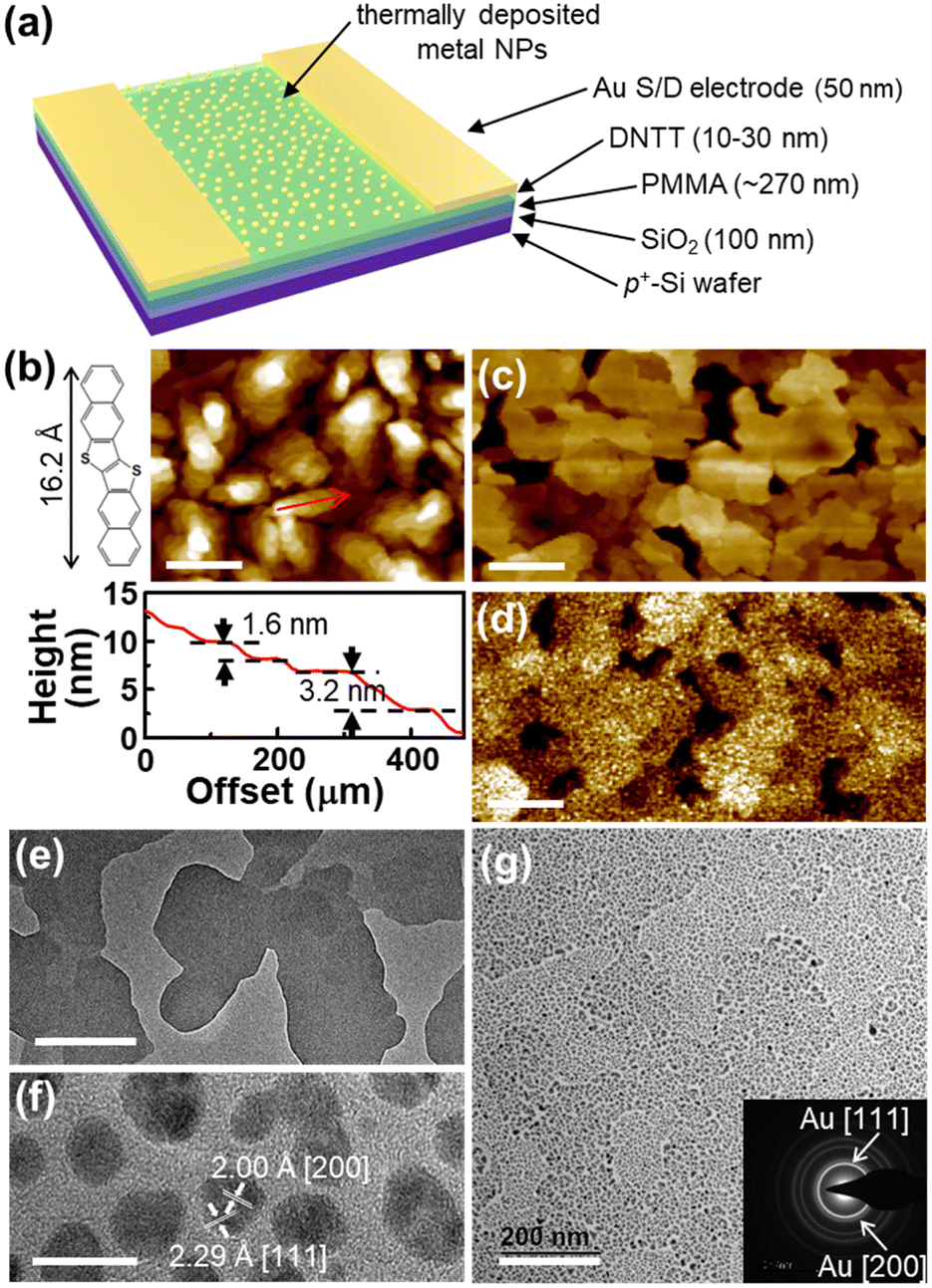 | ||
| Fig. 1 Device scheme and microstructures of DNTT and gold nanoparticles (Au NPs) atop. (a) A schematic illustration of a bottom-gate/top-contact OFET. (b) AFM topography image (top) and height profile (bottom) extracted along the red arrow of 30 nm-thick DNTT film. AFM images of 10-nm thick DNTT film (c) without and (d) with Au metal NPs (scale bars in AFM images denote 500 nm). High-magnification Transmission Electron Microscopy (TEM) images of 10-nm thick DNTT film (e) without and (f) with Au NPs on top. White arrows and lines show the distance values between lattice planes. (g) Low-magnification TEM image of 10-nm thick DNTT film with Au NPs. The inset shows the corresponding selected-area electron diffraction (SAED) pattern. Scale bars in Fig. 1e and g denote 200 nm, while the scale bar in Fig. 1f denotes 10 nm. | ||
The mechanism of NP formation can be understood from previous studies.33 When thermally evaporated metal atoms collide with the DNTT layer and condense, they move across the surface of the DNTT layer, potentially colliding with other vapor atoms to form a nucleus. According to the balance between surface and volume energies, a critical nucleus size exists at which further growth and the formation of a stable nucleus state occur. Following the formation of a stable nucleus, these nuclei grow into islands either through the acquisition of vapor atoms, or through coalescence. If the thermal evaporation process of the metal is stopped before significant coalescence of nuclei occurs, only partially coalesced particles, which are metal NPs, remain, as shown in Fig. 1. These results suggest that each NP is separated in the channel region so that the charge transport between source and drain electrodes still occurs through the channel layer when the device is turned on.
The basic electrical properties of the OFETs were examined by measuring the output and transfer characteristics in dark conditions. As shown in Fig. 2a, these OFETs showed the decreased drain current (ID) in output characteristics, while they maintained nearly ideal linear-to-saturation transitions with minimal contact resistance. Fig. 2b shows typical transfer characteristics of p-channel OFET devices. Note that the hysteresis was relatively small in the DNTT OFET without a metal NP layer, suggesting that the PMMA interlayer effectively passivate the SiO2 surface.34 Interestingly, such a kind of hysteresis was not observed in OFETs with metal NPs, unlike conventional OFET-NP memory devices reported in the previous literature.35,36 This highlights a distinctive feature of our devices that do not afford purely electrical writing or programming. As an additional verification step, we also showed that there were no memory effects even after enlarging programming/erasing biases (Fig. S3, ESI†). The abovementioned behaviour is associated with the device structure. Firstly, the deposition of metal NPs at the top surface of an organic semiconductor layer lead to a big difference. Generally reported OFET memories contain NPs near the interface between semiconductor and insulator layers, where the substantial trapping of charge carriers occurs upon device on/off cycling.20,37 In the present device structure, however, when a negative gate bias (VG) is applied to the gate electrode for the channel formation, any pre-charged NPs on top of the semiconductor layer are effectively emptied without perturbation to the channel transport. Secondly, the absence of a tunnelling layer on each NP is another contributor to the hysteresis-minimized current behaviour. Generally, charge trapping materials (e.g., metal NPs, electrets, floating gates) which are surrounded by an insulating layer exhibit the reduced/controlled leakage of trapped charges.35–38 Those layers provide direct band-to-band tunnelling or a Fowler–Nordheim tunnelling path for charge trapping/detrapping when an appropriate bias is applied, which gives electrically programmable/erasable characteristics to OFETs.36,39 However, in the case of Au or Ag NPs without additional insulating coatings, charge carriers (i.e., holes in a p-type OFET) can be temporarily stored by charging metal NPs but they are naturally detrapped without long-term electrostatic effects. Furthermore, the deposition of metal NPs at the top surface of the organic semiconductor layer could be beneficial for preserving the highly-ordered morphology of the underlying channel material, leading to high on-current and low off-current (Fig. 2b). The field-effect mobilities were extracted at the saturation regime and plotted in Fig. 2c. While the resultant field-effect mobility exhibited a slight decrease after metal NP deposition, the electronic conductivity of DNTT films, measured using the four-point probe method, showed negligible change before and after metal NP deposition (Fig. S4, ESI†). This could be attributed to the partial disruption of the π–π conjugation of the channel material by metal NPs. Nonetheless, the mobility values extracted from OFET devices based on DNTT with Au or Ag NPs atop were still reasonably high, which suggests that metal NPs were marginally penetrated into the semiconducting layer and their overall effect on the charge transport in the organic channel was small.38,40
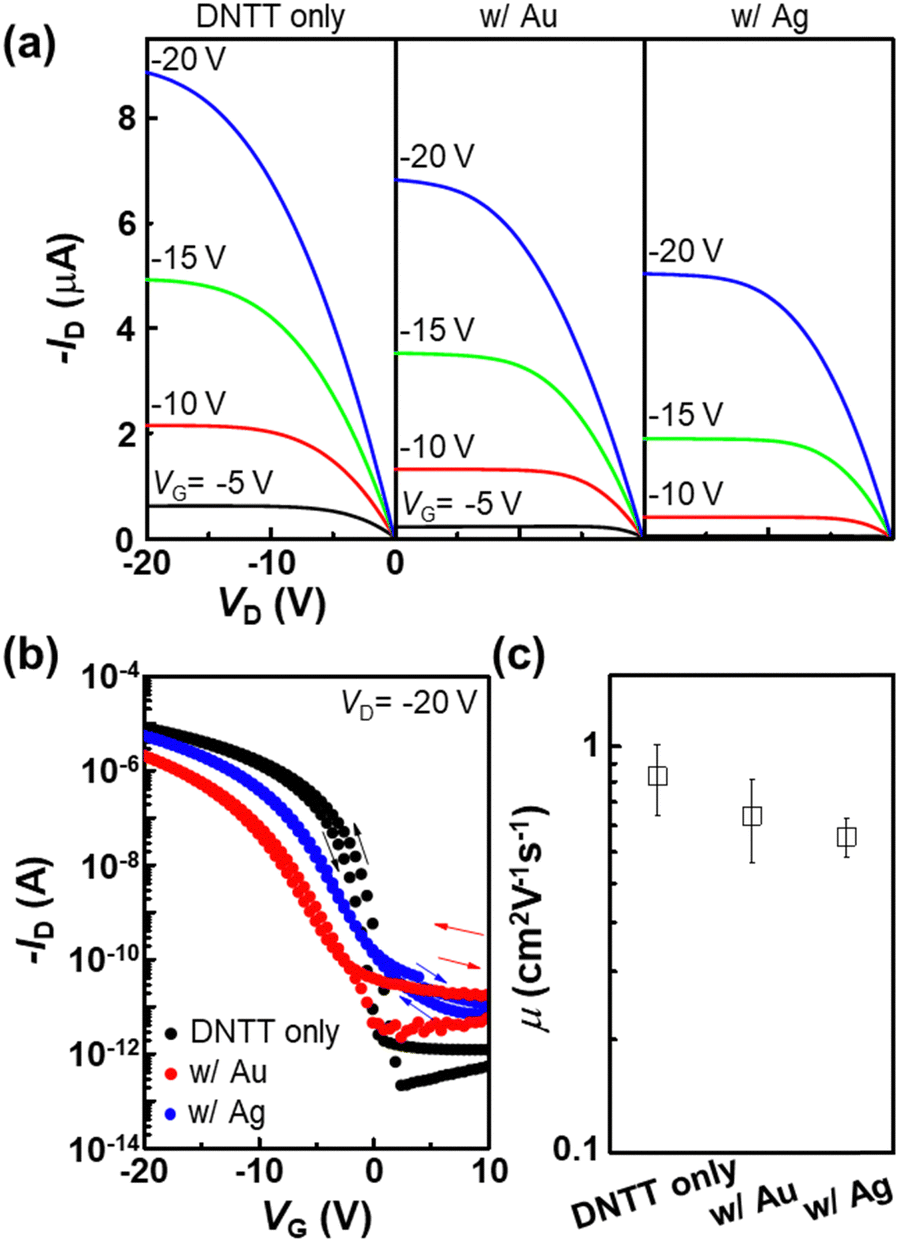 | ||
| Fig. 2 Electrical characterization of DNTT OFETs incorporated with metal NPs. (a) Transistor output characteristics and (b) dual-sweep transfer curves measured in the saturation regime of DNTT OFETs without/with Au or Ag NPs. (c) Field-effect mobilities extracted from OFETs. | ||
The optical characteristics were analysed, beginning with the UV-vis absorption spectra of both pristine and NP-hybridized DNTT films. These films were deposited on PMMA-passivated quartz substrates. The UV-vis absorption spectra of these films are depicted in Fig. 3a. In the pristine sample, only the characteristic absorption peaks of DNTT were observed (as represented by the black line),41 whereas the NP-deposited samples revealed the plasmonic effects of Au or Ag NPs (as discussed below).36,42 The maximum peak of Au NPs exhibited a red shift as the thickness of Au NP layer increased,43,44 with the nominal thickness of the thermally evaporated Au layer estimated to be approximately ∼3 nm, based on previously reported values.36 Notably, both Au and Ag NP deposition enhanced the light absorption of the DNTT layer. However, a significant enhancement was observed primarily from DNTT integrated with Au NPs, which could be attributed to the Au NP layer which was relatively thicker than the Ag NP layer. The differential absorption spectra, normalized by the nominal thickness of the metal layer, indicate that the absorption enhancement is similar for both Au and Ag NP layers as illustrated in Fig. S5 (ESI†).
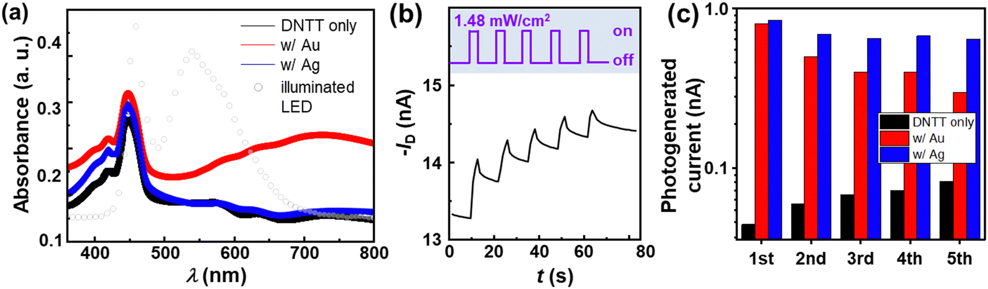 | ||
| Fig. 3 Optoelectronic properties of OFETs incorporating nanoparticles. (a) UV-vis absorption spectra of DNTT films with or without metal NPs. The wavelength spectrum of a broadband white LED source is displayed with open circle. (b) The upper panel indicates the power density of the light pulse applied to the OFET with a Au NPs. The light was illuminated for 3 s at 10 s intervals. The power panel corresponds to the ID measurements at VG = 0 V and VD = −2 V. (c) Photogenerated current calculated from each illumination cycle in short-term transient photocurrent measurements. | ||
Next, we investigated the light-mediated modulation of electrical properties of the DNTT layer by measuring short-term transient photocurrent under white-light illumination. Since the long-term transient photocurrent measurement may include the charge retention characteristics of metal NPs, the short-term transient photocurrent measurement was conducted. Specifically, the ID was recorded at VD = −2 V and VG = 0 V after applying a negative gate bias of VG = −60 V for 60 s so that the residual bias stress effect could be avoided, while the white light was illuminated for 3 s, at every 10 s, total five times. The power density of the illuminated light was set to 1.48 mW cm−2. Fig. 3b shows a representative result of the short-term transient photocurrent measurement. When the light was turned on, the ID increased and when the light was turned off, the ID decreased but it did not return to its initial value even after 10 s. During the photocurrent measurement shown in Fig. 3b, the lifetime of the electron–hole pairs (EHPs) in the DNTT was longer than 10 s, and the 5-time illumination process resulted in an increment of the final ID. Therefore, after the successive light on–off cycles, the final ID increased to a value higher than the initial ID, which could be attributed to the photogenerated charge carriers. Upon the white light illumination, the EHPs are generated in the semiconductor layer via exciton dissociation. Subsequently, the photogenerated electrons and holes can act as charge carriers in the semiconductor under the appropriate VD, leading to an additional current, which is called the photogenerated current. However, the photogenerated current can be eliminated by the recombination of EHPs. Once the light is turned off, the photogenerated carriers are recombined and the resultant photogenerated current is reduced.
For more systematic analysis, we defined the current increment during each illumination step as a photogenerated current and plotted it in Fig. 3c. Note that all DNTT OFETs showed relatively stable and reproducible photogenerated current values during the 5 successive illumination steps. The photogenerated current in the OFETs with a metal NP layer was in the range of 10−9 A during the 5 illumination steps. Considering that the OFETs without the metal NP layer showed a photogenerated current below 10−10 A, the enhanced photocurrent could be attributed to the presence of metal NPs via localized surface plasmon resonance (LSPR) which is an optical phenomenon observed in metal NPs (typically Au or Ag). When the incident light interacts with NPs, the electrons in NPs can be excited to collectively oscillate at specific resonance frequencies.45 This oscillation results in the enhanced absorption of the incident light at a certain wavelength, and the enhanced absorption makes additional photogenerated carriers. Furthermore, the photogenerated current systematically increased with the intensity of the light (Fig. S6, ESI†), indicating strong optoelectronic coupling. This photoinduced modulation of the electrical properties suggests that the current levels of the device can be optically adjustable and employed for optical memory devices that require a clearly identifiable difference in current levels induced by optical stimulation.
The metal NP layer also serves as a charge trapping centre, imparting charge retention characteristics to the OFET devices. To demonstrate the existence of charge retention properties, we examined the residual current level after the cessation of illumination on OFET devices, which was determined by assessing the long-term transient photocurrent. The ID was measured under the same bias conditions as were used for the transient photocurrent measurements. The white light was illuminated for 300 s after measuring the dark current for 30 s. The photogenerated current during light illumination and the immediate current decay after illumination removal were observed in all the OFETs; however, the decay time varied substantially, depending on the device structure. Fig. 4a displays the ID measured from the OFET equipped with a Au NP layer. When the light was turned on, the ID abruptly increased due to photogenerated charge carriers. Once the light was turned off, the ID slightly decreased but remained stable. For comparison, Fig. 4b shows the normalized drain current, ID(t′)/I0, recorded from three different types of OFETs. Note that ID(t′) represents the drain current with post-light deactivation, I0 denotes the drain current level immediately after light deactivation, and t′ signifies the time elapsed since the post-light deactivation. The solid lines correspond to the fitted curves with the stretched exponential model as shown below:46
ID(t′) = I0![[thin space (1/6-em)]](https://www.rsc.org/images/entities/char_2009.gif) exp(−t′/τ)β exp(−t′/τ)β | (1) |
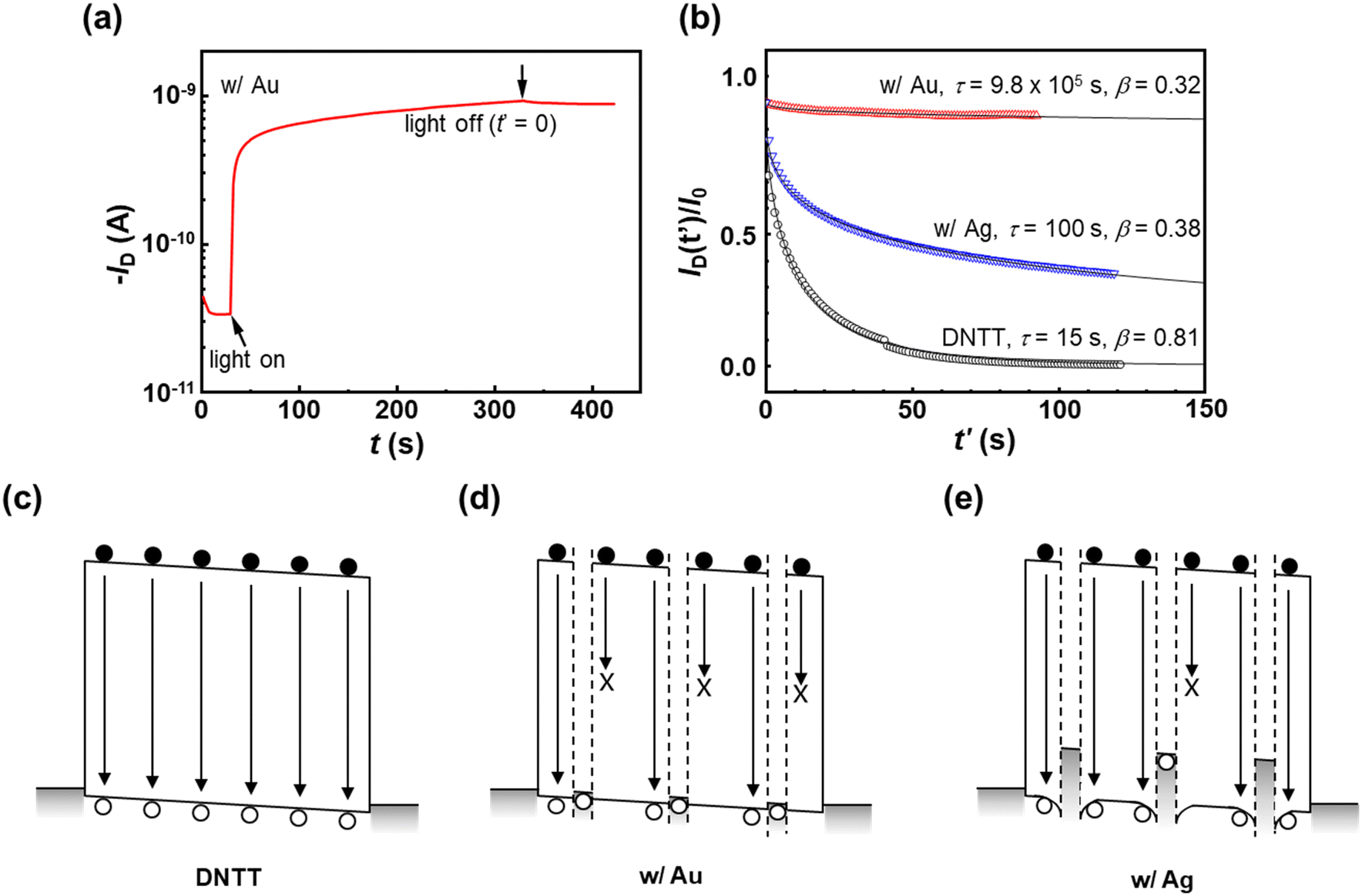 | ||
| Fig. 4 Charge retention characteristics of OFETs incorporating metal nanoparticles and the mechanism of charge trapping and retention. (a) Long-term transient photocurrent measurements at VG = 0 V and VD = −2 V from the OFET with Au NPs. (b) Normalized drain currents measured from OFETs with or without metal NPs, ID(t′)/I0 measured as a function of time, where I0 is the drain current recorded immediately after turning off the illumination. The solid lines are fitted curves with the stretched exponential model according to eqn (1) derived in the text with the fitting parameters, τ and β. (c–e) Schematic demonstration of the current retention mechanism in the OFET with or without metal NPs. Open circles and closed circles denote holes and electrons, respectively. | ||
Fig. 4c–e illustrate the proposed mechanisms governing the retention of photogenerated charge carriers under the influence of an applied VD. Upon light illumination, EHPs are generated and subsequently dissociated into holes and electrons due to the applied VD, inducing a slight tilt in the energy band of the semiconductor layer. However, given the imbalanced charge transport characteristics between electrons and holes in organic semiconductors,47 we hypothesize that only holes will effectively contribute to the current modulation during light illumination and charge trapping. Concentrating on the majority carrier in the semiconductor, we note that holes migrate towards the drain. In the DNTT channel without metal NPs, holes recombine with electrons freely when they encounter each other during the drift, due to the lack of recombination barriers (Fig. 4c); this leads to a rapid decay in photocurrent. Within the DNTT channel equipped with Au NPs (Fig. 4d), as holes migrate toward the drain, they encounter potential wells created by the Fermi level difference between a Au NP and DNTT, leading to their injection into the Au NPs. Once holes are injected, the recombination process is delayed, thereby, allowing the persistence of photocurrent after the deactivation of light. On the other hand, in the case of Ag NPs, a deeper potential well prevents charge carriers from escaping easily (Fig. 4e). However, compared to the case of the DNTT with a Au NP layer, the significant difference in Fermi level between an Ag NP and DNTT increases the barrier height for charge injection. As a result, there is no significant delay in recombination, which leads to less efficient current retention characteristics. This phenomenon illustrates the impact of varying metal NPs on the movement and recombination of photogenerated charge carriers, thus, variations in the resultant current retention behaviour.
Moreover, the distinct trends in photogenerated current observed with an increasing number of light pulses (Fig. 3c) provide new insights into the mechanism of NP-assisted photocurrent generation. In the OFET with only DNTT, an increasing trend in photogenerated current is seen with more light pulses, indicative of trap-passivated photocurrent generation. Upon the first light pulse, photogenerated carriers are trapped at defect sites within the DNTT layer. Subsequent light pulses effectively generate more carriers due to the previously filled trap sites. In contrast, the OFET with Au NP exhibits an opposite trend, showing a decrease in photogenerated current as the number of light pulse increases, suggestive of photocurrent generation constrained by the trapping capacity of NPs. Initially, EHPs generated by the first light pulse are trapped in the metal NPs, reducing recombination in the channel and maintaining high charge carrier concentration. Consequently, carriers generated by subsequent light pulses encounter a scenario where most NPs are already saturated with charge carriers, resulting in the recombination rate exceeding the trapping rate, and thus, a decreasing trend in photogenerated carriers with an increasing number of light pulses.
Regarding the practical utilization of the metal NP-hybridized organic semiconductor system, the average NP size is another important factor to control. To investigate this aspect, we analysed the electrical characteristics of the DNTT OFETs incorporated with Au NPs, while carefully controlling the nominal metal deposition time, thus, the overall Au NP size. The bright-field TEM images shown in Fig. 5a–d vividly depict the DNTT-Au NP layer with various Au deposition times. Notably, with increasing the deposition time, both the coverage area and size of Au NPs increased. The average Au NP sizes measured from the hybrid layers at the deposition time of 15, 30, and 60 s are measured as 5.4 ± 0.8, 5.9 ± 1.4, and 6.7 ± 0.7 nm, respectively (Fig. 5e). As the deposition time increases, the coverage area of Au NPs consistently expanded by 9.6 to 45.9% (Fig. 5f). Additionally, the average distance among Au NPs emerged as another key factor. Fig. 5g illustrates that the greatest interparticle distance was observed in the DNTT-Au NP hybrid layer with the shortest Au deposition time (15 s). This average distance, 7.9 ± 3.6 nm, is nearly 2.8 times larger than those measured at the deposition time of 30 and 60 s. The abovementioned findings suggest that the nucleation of Au NP predominantly occurs at the initial deposition phase (15 to 30 s), while the NP growth prevails during the latter deposition stage (30 s to 60 s).
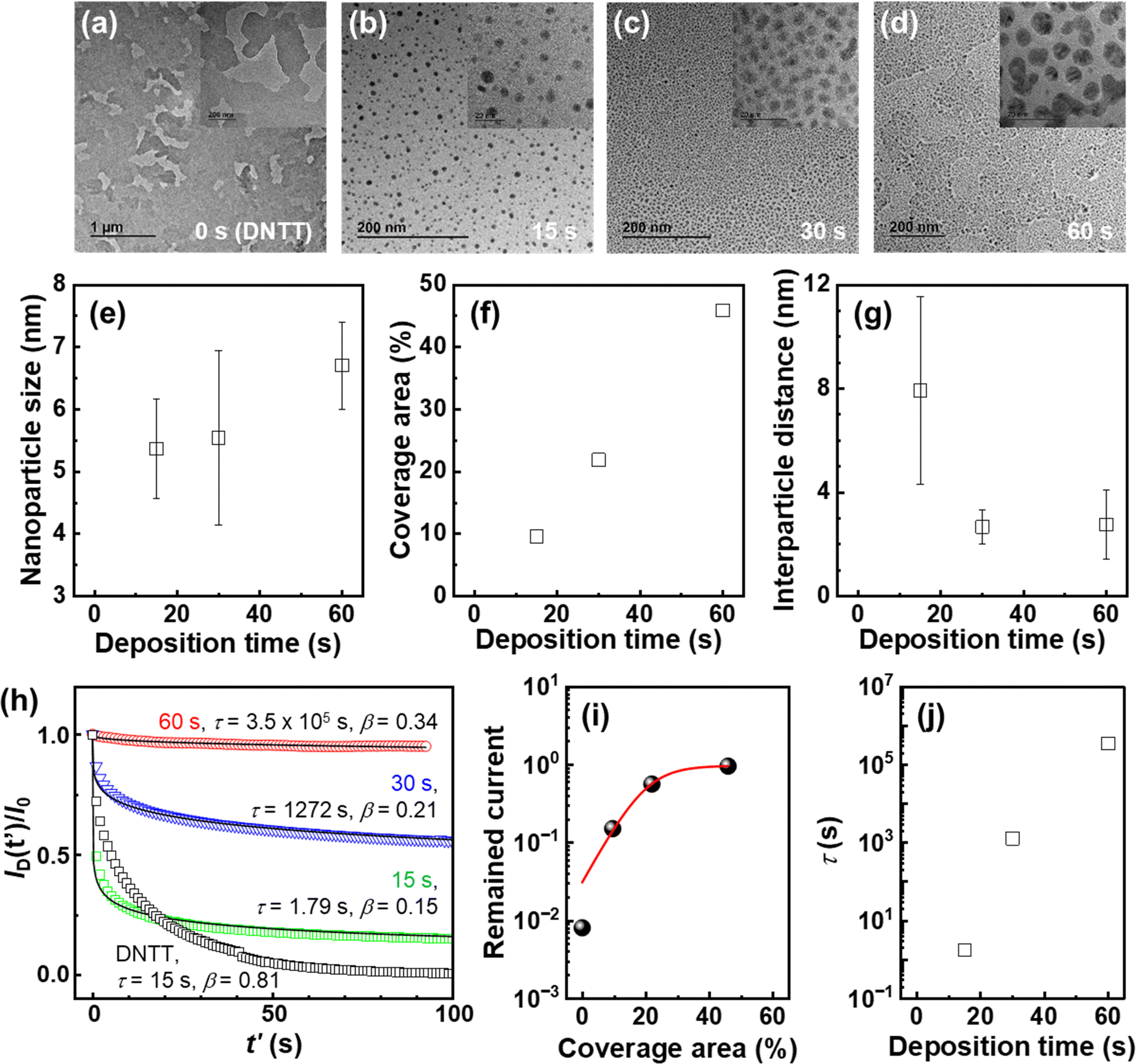 | ||
| Fig. 5 Effects of Au nanoparticle morphology in DNTT layers on charge trapping and retention characteristics. Bright-field TEM images displaying: (a) pristine DNTT, DNTT layer with deposition times of (b) 15 s, (c) 30 s, and (d) 60 s. The inset shows an enlarged view. Plots illustrating: (e) nanoparticle size, (f) coverage area, and (g) interparticle distance in relation to metal deposition time. (h) Long-term transient photocurrent measurements at VG = 0 V and VD = −2 V in OFETs with varying deposition times of Au NPs. The normalized drain current, ID(t′)/I0 plotted as a function of time, where I0 represents the drain current immediately after light deactivation. Solid lines represent stretched exponential fits using eqn (1) as explained in the text, with indicated fitting parameters τ and β. (i) Relationship between the remaining current ratio obtained from (h) at t′ = 90 s and the coverage area. (j) Dependence of decay time constant values, acquired from exponential fits, on metal desposition time. | ||
In order to delve deeper into the impact of NP size, coverage, and interparticle distance on the resultant OFET characteristics, we conducted a detailed analysis of the long-term transient photocurrent in DNTT-Au hybrid OFETs with varying metal deposition times. As shown in Fig. 5h, the normalized drain current after the light cessation, ID(t′)/I0, is displayed for hybrid OFETs subjected to different metal deposition times. The hybrid OFET with 60-s Au deposition exhibited the highest ID(t′)/I0 value of approximately 0.95 after 90 s, followed by the hybrid OFET with 30-s (∼0.56) and 15-s Au deposition (∼0.15), and finally by the pristine DNTT OFET (0.008, 0-s Au deposition) as indicated in Fig. S8 (ESI†). Although ID(t′)/I0 were plotted as a function of the average NP size and interparticle distance, no clear correlation between these parameters emerged (Fig. S9a and b, ESI†). However, a distinct trend in ID(t′)/I0 values emerged when they were plotted as a function of the surface area covered by NPs on a logarithmic scale, closely resembling a logistic function (red line in Fig. 5i and Fig. S9c, ESI†). The logistic function is commonly employed to describe the population growth of a system constrained by limited resources, a concept applicable in the context of interface atomic profiles of distinct layers grown by sputtering.48,49 In our study, the remained current value is analogous to the population of this system, as it represents the number of charge carriers trapped in the NPs. As the coverage area of NP increases, their charge trapping capability also increases by eventually saturates due to the finite charge trapping capacity of the metal NPs.37 Therefore, the logistic function is an appropriate model to describe the remained current value trapped in the metal NPs as a function of their coverage area. Remarkably, this behaviour can be meticulously regulated by adjusting the metal deposition time.
The decay time constant (τ) values obtained from fitting also demonstrate its correlation with the NP deposition time. As depicted in Fig. 5j, the OFET with a 60 s deposition time showed the highest τ value, 3.5 × 10⁵ s, followed by the OFETs with deposition times of 30 s (1.3 × 10³ s) and 15 s (1.8 s). Even when the metal deposition time extends to 120 s, the OFET continues to exhibit a photo-response, with the retention time further increasing to 8.2 × 10⁶ s (Fig. S10, ESI†). However, once the deposition time exceeds 200 s, no significant photo-response is observed, even in short-term transient photocurrent measurements (Fig. S10, ESI†). In contrast, the neat DNTT OFETs displayed a τ value (15 s) which is higher than that of the 15 s deposition sample. This divergence could be attributed to a distinct charge retention mechanism arising from metal NPs on the DNTT surface (vide infra). Consequently, our comparison was confined to NP-containing samples to observe the impact of NP morphology on τ values. The τ value is anticipated to be influenced by the average NP size, interparticle distance, and NP-covered area. An increase in the interparticle distance elevates the probability of recombination, while alterations in the NP-covered area50 and the average NP size lead to the augmentation in charge trapping density.37 This trend is evident in Fig. S11 (ESI†). During the initial stage (15–30 s), the τ value increases substantially (700 times). Among the abovementioned three factors, the most notable rate of change occurred with the change in interparticle distance (70% decrease), followed by a 10% increase with that in NP-covered area and a 3% increase with that in average NP size. Consequently, the reduced recombination probability due to the decreased interparticle distance and the augmented trapping density resulting from increased NP coverage were the primary contributions to the τ value variation. At the growing stage (30–60 s), the τ value increase became relatively less pronounced (300 times). Here, the most substantial rate change was observed with the change in NP-covered area (24% increase), followed by those in average NP size (21%) and interparticle distance (4%). Unlike the initial stage, the change in interparticle distance decreases markedly. Nonetheless, it is inferred that the overall τ value increase is influenced by the increased trapping density due to the changes in NP coverage and average size. If the metal deposition time becomes excessively long, an interconnected network between individual NPs forms. This interconnected metal layer no longer functions as a charge trapping centre, but instead creates a connection between the source and drain electrodes. Consequently, the device exhibits no photo-response under light pulse illumination (Fig. S10a, ESI†) and fails to demonstrate transfer characteristics (Fig. S10b, ESI†). Thus, it is evident that all factors cumulatively contribute to the observed effects although it is tricky to clearly distinguish the impacts of individual morphological factors.
The additional analysis and possible applications for each deposition time range were examined. As illustrated in Fig. 5h, it is notable that the DNTT OFET exhibits a slower photocurrent decay compared to the case with a 15 s deposition time. Despite the presence of small-sized or low-density NPs, the plasmonic effect in proximity to NPs induces a transient increase in light absorption, consequently, leading to the increased recombination of photogenerated carriers compared to the pristine DNTT OFETs. These devices lack LSPR centres, which results in low photocurrents, a reduced probability of recombination, and finally higher τ values (slower decay of photogenerated current). Therefore, owing to the modest NP size and limited trapping characteristics, the current retention is insignificant in samples prepared with minimal NP deposition time. The accelerated photocurrent decay, stemming from an enhanced recombination rate, renders them apt for use as photonic sensors. For the 30-s deposition case, the increased trapping density compared to the 15-s case results in the augmented current retention, albeit without an exceedingly high τ value. This scenario is favourable for neuromorphic transistors, and it is envisaged that device characteristics can be effectively modulated, and the desired neuromorphic traits can be fine-tuned by simply adjusting metal deposition time on top of an organic channel layer.
In the context of 60 s deposition, where a substantial area is covered by metal NPs and the average interparticle distance is decreased, the recombination probability diminishes while the number of trapping sites surges, resulting in exceptional charge retention properties. To provide a straightforward demonstration, we conducted repetitive optical programming and electrical erasing processes on both OFETs: one with a 60 s deposition time for Au NPs and the other without any metal deposition, to verify the reproducibility of current retention. The outcomes are presented in Fig. S12 (ESI†). The OFET containing Au NPs reveals a remaining ID approaching 10−9 A, marked by red squares in the initial graph, following optical programming as indicated by light blue. Upon applying VG = −60 V for 60 s (electrical erasing, indicated by light orange), the ID diminishes to ∼2 × 10⁻¹⁰ A. The consistency of each current state is verified through subsequent optical programming and electrical erasing cycles. It is noteworthy that the discrepancies in the current states slightly intensify compared to those observed after the inaugural cycle. Consequently, OFETs with a 60 s deposition time for Au NPs hold a potential for non-volatile memory applications. Furthermore, there is also an expectation of enhancing memory performance with superior retention properties through meticulous control over NP coverage and interparticle distance.
Thus, by tailoring NP morphology and type with a conventional metal deposition technique, it is feasible to achieve the fine control over charge trapping density and recombination rate in OFET devices. Consequently, diverse devices with desired attributes can be obtained by simply manipulating the metal deposition time. These devices can span various domains, including sensors, neuromorphic transistors, and memory devices. This approach simplifies phototransistor fabrication processes and broadens the scope of metal NP-hybridized OFET devices.
Conclusions
In this research, we developed optically programmable organic field-effect transistors by combining a conventional OFET device structure with a vacuum-deposited metal NP layer. The incorporation of metal NPs on top of a DNTT-based semiconducting layer showed minimal interferences with the inherent charge transport efficiency in the OFETs. However, it was revealed that the photogenerated current could be enhanced nearly tenfold due to the LSPR effect of noble metal NPs on the DNTT surface. Remarkably, these noble metal NPs serve as centres for both charge trapping and retention, thereby, enabling tailored optical programming in an OFET device structure. The demonstration of versatile functions of DNTT-NP hybrid OFET devices may significantly contribute to the broadening of OFET's applications to not only photosensors but also promising drivers in future information technology such as non-volatile memories, photo-programmable transistors, neuromorphic devices, etc.Author contributions
J. H. K. and C.-H. K. conceived and designed the experiments. Device fabrication, data acquisition/analysis was performed by J. H. K., I.-Y. J., S. B., H.-r. C., S. P. and J. L. The project was coordinated by M.-H. Y. The manuscript was written by J. H. K. and I.-Y. J. and revised by S. P., C.-H. K. and M.-H. Y. All authors contributed to the manuscript and have given approval to the final version of the manuscript.Conflicts of interest
There are no conflicts to declare.Acknowledgements
M.-H. Y. acknowledges support from a National Research Foundation (NRF) grant funded by the Korean government (MSIT) (NRF-2020M1A2A2080748, NRF-2022M3C1C5A01097681, and NRF-2021R1A2C1013015).References
- M. Kaltenbrunner, T. Sekitani, J. Reeder, T. Yokota, K. Kuribara, T. Tokuhara, M. Drack, R. Schwödiauer, I. Graz, S. Bauer-Gogonea, S. Bauer and T. Someya, Nature, 2013, 499, 458–463 CrossRef CAS PubMed.
- A. Grimoldi, L. Colella, L. La Monaca, G. Azzellino, M. Caironi, C. Bertarelli, D. Natali and M. Sampietro, Org. Electron., 2016, 36, 29–34 CrossRef CAS.
- S.-Y. Hsiao, H.-L. Lin, W.-H. Lee, W.-L. Tsai, K.-M. Chiang, W.-Y. Liao, C.-Z. Ren-Wu, C.-Y. Chen and H.-W. Lin, Adv. Mater., 2016, 28, 7013 CrossRef CAS PubMed.
- M. Kunii, H. Iino and J. I. Hanna, IEEE Electron Device Lett., 2016, 37, 486–488 CAS.
- C. Zhang, J. Zhang, W. Zeng, N. Zheng, W. Li, W. Gao, G. Yu and C. Yang, Polym. Chem., 2016, 7, 2808 RSC.
- L. Feng, W. Tang, J. Zhao, R. Yang, W. Hu, Q. Li, R. Wang and X. Guo, Sci. Rep., 2016, 6, 20671 CrossRef CAS PubMed.
- R. Komatsu, H. Sasabe, Y. Seino, K. Nakao and J. Kido, J. Mater. Chem. C, 2016, 4, 2274–2278 RSC.
- R. Komatsu, H. Sasabe, K. Nakao, Y. Hayasaka, T. Ohsawa and J. Kido, Adv. Opt. Mater., 2017, 5, 1600675 CrossRef.
- T. Basel, D. Sun, S. Baniya, R. McLaughlin, H. Choi, O. Kwon and Z. V. Vardeny, Adv. Electron. Mater., 2016, 2, 1500248 CrossRef.
- J. Jean, A. Wang and V. Bulović, Org. Electron., 2016, 31, 120–126 CrossRef CAS.
- T. M. Grant, T. Gorisse, O. Dautel, G. Wantz and B. H. Lessard, J. Mater. Chem. A, 2017, 5, 1581–1587 RSC.
- G. Nan, X. Zhang and G. Lu, Phys. Chem. Chem. Phys., 2016, 18, 17546–17556 RSC.
- S. H. Yu, J. Cho, K. M. Sim, J. U. Ha and D. S. Chung, ACS Appl. Mater. Interfaces, 2016, 8, 6570–6576 CrossRef CAS PubMed.
- R. O. Ocaya, A. Al-Ghamdi, K. Mensah-Darkwa, R. K. Gupta, W. Farooq and F. Yakuphanoglu, Synth. Met., 2016, 213, 65–72 CrossRef CAS.
- K.-J. Baeg, Y.-Y. Noh, J. Ghim, B. Lim and D.-Y. Kim, Adv. Funct. Mater., 2008, 18, 3678–3685 CrossRef CAS.
- Y.-L. Liu, Q.-D. Ling, E.-T. Kang, K.-G. Neoh, D.-J. Liaw, K.-L. Wang, W.-T. Liou, C.-X. Zhu and D. S.-H. Chan, J. Appl. Phys., 2009, 105, 044501 CrossRef.
- T.-K. Kang, Sci. Rep., 2016, 6, 24406 CrossRef CAS PubMed.
- B. J. Kim, Y. Ko, J. H. Cho and J. Cho, Small, 2013, 9, 3784–3791 CrossRef CAS PubMed.
- W. L. Leong, N. Mathews, B. Tan, S. Vaidyanathan, F. Dötz and S. Mhaisalkar, J. Mater. Chem., 2011, 21, 5203–5214 RSC.
- C.-H. Kim, S. Sung and M.-H. Yoon, Sci. Rep., 2016, 6, 33355 CrossRef CAS PubMed.
- V. Tischler, P. Dudek, J. Wijekoon, L. A. Majewski, Y. Takeda, S. Tokito and M. L. Turner, Org. Electron., 2023, 113, 106685 CrossRef CAS.
- H. Sirringhaus, Adv. Mater., 2009, 21, 3859–3873 CrossRef CAS.
- M. Matters, D. M. de Leeuw, P. T. Herwig and A. R. Brown, Synth. Met., 1999, 102, 998–999 CrossRef CAS.
- K. Pei, X. Ren, Z. Zhou, Z. Zhang, X. Ji and P. K. L. Chan, Adv. Mater., 2018, 30, 1706647 CrossRef PubMed.
- C. Qian, J. Sun, L. Kong, Y. Fu, Y. Chen, K. Wang, S. Wang, H. Xie, H. Huang, J. Yang and Y. Gao, ACS Photonics, 2017, 4, 2573–2579 CrossRef CAS.
- Y. J. Jeong, D.-J. Yun, S. H. Kim, J. Jang and C. E. Park, ACS Appl. Mater. Interfaces, 2017, 9, 11759–11769 CrossRef CAS PubMed.
- J.-Y. Chen, Y.-C. Chiu, Y.-T. Li, C.-C. Chueh and W.-C. Chen, Adv. Mater., 2017, 29, 1702217 CrossRef PubMed.
- L. Zhou, S.-T. Han, S. Shu, J. Zhuang, Y. Yan, Q.-J. Sun, Y. Zhou and V. A. L. Roy, ACS Appl. Mater. Interfaces, 2017, 39, 34101–34110 CrossRef PubMed.
- R. F. Pierret, Semiconductor Device Fundamentals, Addison-Wesley, Boston, 1996 Search PubMed.
- H. Sirringhaus, Adv. Mater., 2005, 17, 2411–2425 CrossRef CAS.
- G. Horowitz and M. E. Hajlaoui, Synth. Met., 2001, 122, 185–189 CrossRef CAS.
- W. Xie, K. Willa, Y. Wu, R. Häusermann, K. Takimiya, B. Batlogg and C. D. Frisbie, Adv. Mater., 2013, 25, 3478–3484 CrossRef CAS PubMed.
- K. L. Chopra and M. R. Randlett, J. Appl. Phys., 1968, 39, 1874–1881 CrossRef CAS.
- Y. Yun, C. Pearson and M. C. Petty, J. Appl. Phys., 2009, 105, 034508 CrossRef.
- K. Lee, M. Weis, D. Taguchi, T. Manaka and M. Iwamoto, Chem. Phys. Lett., 2012, 551, 105–110 CrossRef CAS.
- K.-J. Baeg, Y.-Y. Noh, H. Sirringhaus and D.-Y. Kim, Adv. Funct. Mater., 2010, 20, 224–230 CrossRef CAS.
- C.-H. Kim, G. Bhak, J. Lee, S. Sung, S. Park, S. R. Paik and M.-H. Yoon, ACS Appl. Mater. Interfaces, 2016, 8, 11898–11903 CrossRef CAS PubMed.
- S.-J. Kim and J.-S. Lee, Nano Lett., 2010, 10, 2884–2890 CrossRef CAS PubMed.
- Y.-S. Park and J.-S. Lee, Adv. Mater., 2015, 27, 706–711 CrossRef CAS PubMed.
- H.-C. Chang, C.-L. Liu and W.-C. Chen, ACS Appl. Mater. Interfaces, 2013, 5, 13180–13187 CrossRef CAS PubMed.
- T. Yamamoto and K. Takimiya, J. Am. Chem. Soc., 2007, 129, 2224–2225 CrossRef CAS PubMed.
- X. Ren, X. Meng and F. Tang, Sens. Actuators, B, 2005, 110, 358–363 CrossRef CAS.
- T. A. El-Brolossy, T. Abdallah, M. B. Mohamed, S. Abdallah, K. Easawi, S. Negm and H. Talaat, Eur. Phys. J.: Spec. Top., 2008, 153, 361–364 Search PubMed.
- S. Link and M. A. El-Sayed, J. Phys. Chem. B, 1999, 103, 8410–8426 CrossRef CAS.
- K. M. Mayer and J. H. Hafner, Chem. Rev., 2011, 111, 3828–3857 CrossRef CAS PubMed.
- Y. Chen and V. Podzorov, Adv. Mater., 2012, 24, 2679–2684 CrossRef CAS PubMed.
- C.-H. Kim and I. Kymissis, J. Mater. Chem. C, 2017, 5, 4598–4613 RSC.
- A. Chandrasekaran, R. W. E. Van De Kruijs, J. M. Sturm, A. A. Zameshin and F. Bijkerk, ACS Appl. Mater. Interfaces, 2019, 11, 46311–46326 CrossRef CAS PubMed.
- G. P. Chambers and B. D. Sartwell, Surf. Interface Anal., 1990, 15, 126–134 CrossRef CAS.
- R. Xiao, Y. Hou, M. Law and D. Yu, J. Phys. Chem. C, 2018, 122, 18356–18364 CrossRef CAS.
Footnotes |
| † Electronic supplementary information (ESI) available. See DOI: https://doi.org/10.1039/d3tc03609j |
| ‡ These authors contributed equally to this research. |
| This journal is © The Royal Society of Chemistry 2024 |