
 Open Access Article
 This Open Access Article is licensed under a
 Creative Commons Attribution 3.0 Unported Licence
Highly stable semitransparent solar cell employing graphene/WS2/LaVO3 vertical-heterostructure†
Da Hee
Kim‡
ab,
Dong Hee
Shin‡
c,
Dae Ho
Jung
ad,
Si Duck
Oh
e,
Eun Ji
Kim
ab and
Hosun
Lee
 *abd
*abd
aDepartment of Applied Physics, Kyung Hee University, Yongin 17104, Republic of Korea. E-mail: hlee@khu.ac.kr
bEducation Institute for Frontier Science and Technology (BK21 Four), Kyung Hee University, Yongin 17104, Republic of Korea
cDepartment of Smart Sensors Engineering, Andong National University, Andong, Gyeongbuk 36729, Republic of Korea
dInstitute of Natural Sciences, Kyung Hee University, Yongin 17104, Republic of Korea
eSmart Energy and Nano Photonics R&D Group, Korea Institute of Industrial Technology (KITECH), Gwangju, 61012, Republic of Korea
First published on 23rd January 2024
Abstract
Semi-transparent (ST) solar cells are attracting a lot of attention among researchers as they can effectively utilize solar energy in various fields such as building-integrated solar power generation and portable solar chargers. Here, we introduce an ST solar cell composed of triethylenetetramine (TETA)-doped graphene (Gr), WS2, and LaVO3. The device not only harvests solar energy thanks to its high light absorption in the ultraviolet-visible range but is also translucent due to its thin film composition. The photovoltaic parameters and average visible transmittance (AVT) of TETA-Gr/WS2/LaVO3 solar cells are highly dependent on the LaVO3 film thickness (t). Considering the correlation between efficiency and visual effects, the device has power conversion efficiency (PCE) of 5.07% and 35% AVT at t = 200 nm, suggesting that it is suitable for ST solar cells. To maximize the translucent properties of the device, the PCE of the device was further improved to 5.64% by using an Al reflective mirror. The durability of the cell was confirmed to maintain 91 and 84% of the original PCE even under continuous illumination of 1 Sun at 60 °C temperature (Ta) and 30% relative humidity (RH) and 80 °C Ta/50% RH for 1000 h.
1. Introduction
Solar energy with its advantages of cleanliness, abundance, and accessibility, is emerging as one of the leading sources of renewable energy and one of the candidates to meet the future demand of the world.1 For the continued growth of solar energy, the relatively low energy density of solar lighting must be addressed. An approach for increasing energy density is to manufacture semitransparent (ST) solar modules and integrate them into the undesirable transparent surfaces of skyscrapers and automobiles.2 To prepare an effective ST solar cell, it is necessary to simultaneously satisfy optimized power conversion efficiency (PCE) and high average visible transmittance (AVT). Meanwhile, Si solar cells have high efficiency and excellent long-term stability, but their high reflectance requires additional processing and has limited visual effects, making them unsuitable for translucent solar cells. From this point of view, organic- and perovskite-based solar cells have been spotlighted as the most promising candidates for ST solar cells.3–12 Both solar cells have many advantages such as simple device fabrication at low cost, lightweight, and high efficiency, but their commercialization is still limited due to low durability in the atmosphere.13–16Meanwhile, LaVO3 film, one of the perovskite oxide materials, was introduced as an optimized material for the active layer of solar cells due to its high absorption coefficient in the ultraviolet (UV)-visible region.17–19 LaVO3 films with high absorption can be thinned and are suitable as active layers for translucent devices. Additionally, LaVO3 materials are easy to supply and the price is economical.20 Besides, the stability of LaVO3-based optoelectronic devices has already been verified under atmospheric conditions as previously reported in the literature.21–24 On the other hand, two-dimensional (2D) materials such as WS2 are attracting much attention as optoelectronic devices owing to their strong light-material interactions useful for light absorption, noticeable band gaps, and high electron mobility.
Considering the advantages of 2D and LaVO3 films, the 2D/LaVO3 heterojunction structure is expected to provide better properties than single-component material-based optoelectronic devices.24 Most recently, we successfully fabricated a chemical vapor deposition (CVD)-MoS2/LaVO3-based high-performance self-powered photodetector, demonstrating superior performance over other CVD-MoS2-based devices.24 Additionally, the same structural device showed photovoltaic properties under 1 sun (100 mW cm−2) illumination. In previous literature, we mentioned triethylenetetramine (TETA)- doped graphene (Gr) transparent conductive electrodes (TCEs).25–27 TETA-Gr obtained excellent transmittance (T) at the wavelength of 300–1000 nm and low sheet resistance as well as n-type characteristics. Furthermore, TETA-Gr suggests long-term stability in the air and heat.28 Considering the properties of each material, we selected a translucent active layer for WS2 and LaVO3 and a TCE for TETA-Gr. In other words, We fabricated TETA-Gr as a TCE for WS2/LaVO3 devices to maximize the properties of ST solar cells.
Here, WS2 and LaVO3 materials were elaborately selected to fabricate ST solar cells. In the TETA-Gr/WS2/LaVO3 heterojunction structure, efficient translucent solar cells were achieved by fine-tuning the thickness (t) of LaVO3 from 70 to 300 nm. The PCE and AVT values of the ST cell can be tuned from 2.66 to 5.42% and from 55 to 26% as the LaVO3 layer t increases from 70 to 300 nm. Furthermore, the efficiency was improved by 12% by adding an Al reflective mirror for the device with t = 200 nm. Finally, the durability of the device shows that the initial efficiency decreases by only 9 and 16% after 1000 h for 60 °C temperature (Ta) and 30% relative humidity (RH) and 80 °C Ta/50% RH under continuous air mass (AM) of 1.5 global (1 sun, 100 mW cm−2), thereby indicating good stability.
2. Experimental section
2.1 Fabrication of graphene/WS2/LaVO3 semitransparent solar cells
To synthesize the LaVO3 film on the quartz substrate, we used 50 W radio frequency sputtering equipment under an H2 (35%)/Ar mixture gas atmosphere. Here, we varied the thickness of the LaVO3 film by adjusting the sputtering time. Next, WS2 was transferred onto the LaVO3 film using a poly(methyl methacrylate) (PMMA) support film-based wet transfer method.29 Here, the CVD-WS2 sheet was purchased from Six Carbon Technology and is a uniformly grown sample on a SiO2/Si substrate. PMMA-coated WS2/SiO2/Si samples were suspended in a buffered oxide etch bath to separate the SiO2/Si substrate and washed several times in a deionized water bath. Sequentially, the CVD-monolayer Gr was transferred onto the WS2 sheet by the same wet transfer process to finally fabricate the Gr/WS2/LaVO3 heterojunction structure. To prepare n-type Gr, a solution of TETA was dropped on the surface of Gr, followed by spin coating at 2500 rpm for 1 min. Then, the samples were dried at 75 °C for 10 min. TETA solutions were prepared by dissolving TETA molecules in ethanol. To finally complete the solar cell, Ag and Au films were used as the upper and lower electrodes, respectively. We fixed the active area of the devices to 20 × 20 mm2.2.2 Characterizations
The thicknesses of the LaVO3 films were analyzed by field-emission scanning electron microscopy (FE-SEM) (Carl Zeiss, model LEO SUPRA 55). By atomic force microscopy (AFM, Park Systems), we checked the surface roughness of LaVO3. The Raman spectra of WS2 and TETA-Gr were measured by a Raman spectroscopy system with a 532 nm laser. To confirm the uniform WS2 sheet, we observed it through an optical microscope. The transmittance (T)/absorbance spectra of LaVO3, WS2, and TETA-Gr were analyzed by a UV-visible-near-infrared (NIR) spectrophotometer (Agilent Varian, model Carry 5000). The baseline was calibrated with a quartz substrate. With the 4-probe using van der Pauw method (Dasol Eng., model FPP-HS8-40K) and Kelvin probe force microscopy (KPFM) (Park systems, model XE100), we measured the sheet resistance and work function, respectively. To check the atomic bonding state of TETA-Gr, we measured and analyzed the spectrum by X-ray photoelectron spectroscopy (XPS) using an Al Kα line with 1486.6 eV. The photovoltaic parameters of the device were measured using a Keithley 2400 source meter under 1 Sun (100 mW cm−2) illumination in the atmosphere. External quantum efficiency (EQE) was measured from wavelengths of 300–1000 nm from a system consisting of a monochromator and a light source and then calibrated from a commercial Si reference cell. To improve the efficiency of the device by reflecting light transmitted from the translucent solar cell, we used an Al reflective mirror.3. Results and discussion
Fig. 1(a) presents real images of LaVO3 films as a function of t. In Fig. 1(b), the average surface roughness (Rq) of 200 nm LaVO3 is 0.421 nm, suggesting a relatively low roughness. From the cross-sectional FE-SEM image, it is indicated that 200 nm-LaVO3 was grown uniformly, as shown in Fig. 1(c). Fig. 1(d) shows the XPS spectrum for LaVO3 film at t = 200 nm. As shown in the XPS spectrum, the La 3d, V 2p, and O 1s core levels were observed, indicating that the LaVO3 film was well synthesized. Fig. 1(e) and (f) shows the T/absorbance of LaVO3/quartz for various t in the wavelength range of 300 to 1000 nm. With increasing t, the T spectrum gradually decreases while the absorbance spectrum gradually increases. In the T spectrum, the AVT corresponding to the wavelength of 400–800 nm decreases from 67 to 37% with increasing t from 70 to 300 nm.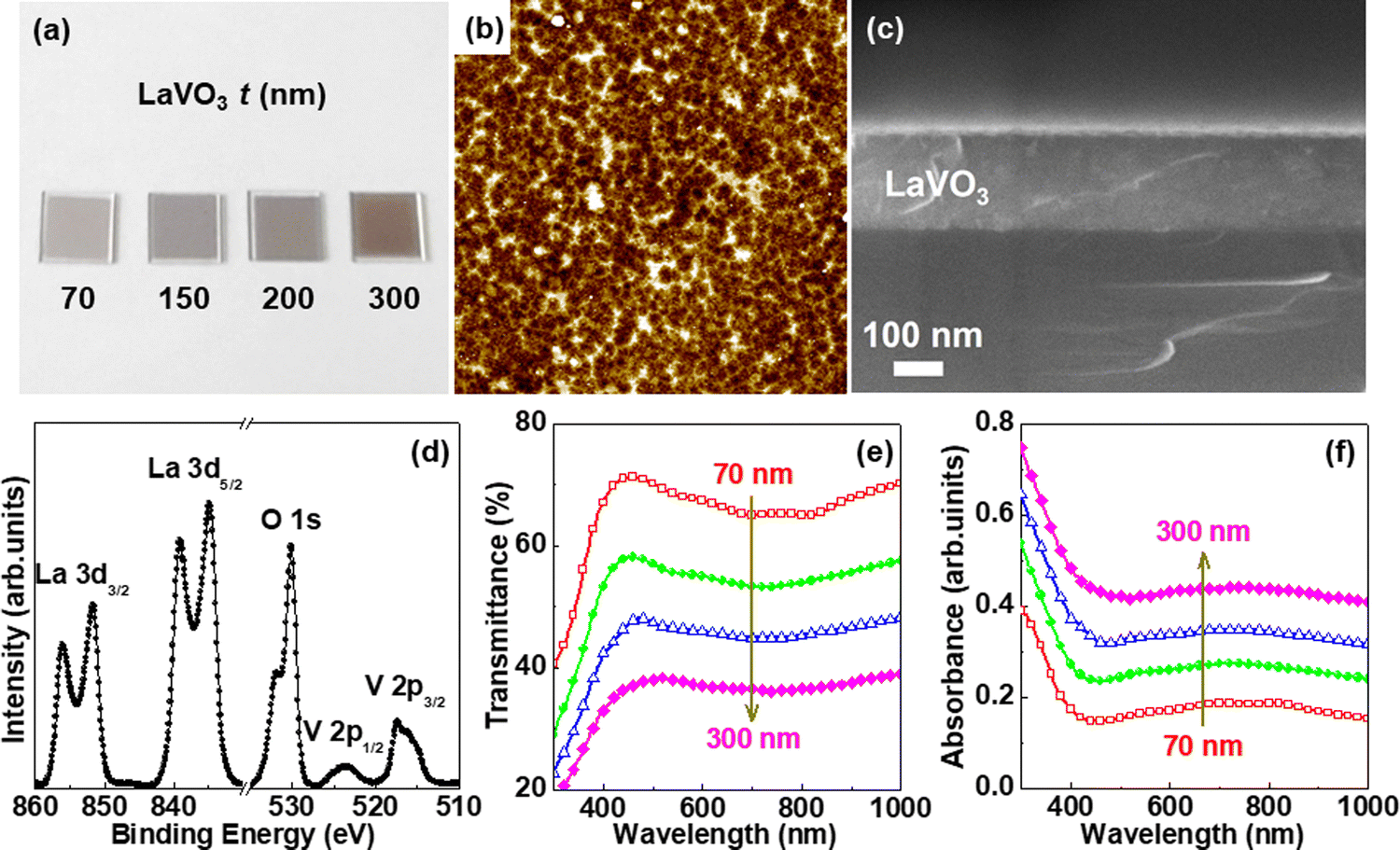 | ||
| Fig. 1 (a) Real image of LaVO3 film on quartz substrate as a function of t. (b) AFM topography image, (c) Cross-sectional SEM image, and (d) XPS spectrum of LaVO3 film at t = 200 nm. (e) Transmittance and (f) Absorbance spectra of LaVO3 film from wavelength of 300 to 1000 nm for various t. | ||
We confirmed that the WS2 sheets grew uniformly without pinholes by optical microscopy (Fig. S1a, ESI†). To confirm the t of the WS2 film, we measured it to be about 3.8 nm by the line profile of the AFM topography image. (Fig. S1b, ESI†). In the XPS spectrum for WS2, well-known peaks of W 4f7/2, W 4f5/2, W 5p3/2, S 2p3/2, and S 2p1/2 were identified (Fig. S1c and d, ESI†). From the XPS spectrum, the atomic ratio of W and S was calculated to be 1![[thin space (1/6-em)]](https://www.rsc.org/images/entities/char_2009.gif) :2, similar to the nominal stoichiometry of WS2.30 In the Raman spectrum for the WS2 sheet, the representative E12g and A1g peaks were identified (Fig. S1e, ESI†). To confirm the number of layers of the WS2 sheet, we evaluated the difference between the peak positions of E12g and A1g, thereby confirming that it was 4–5 layers,31,32 consistent with the AFM results. To confirm the exact Fermi level of multilayer WS2, we measured the work function using the KFPM and obtained 4.58 ± 0.03 eV (Fig. S1f, ESI†). The spectrum for the T and absorbance of the WS2 film in the range of wavelength of 300 to 1000 nm is shown. (Fig. S1g, ESI†). As shown in the spectrum, T and absorbance show opposite trends. We suggest that WS2 is a suitable material for translucent optoelectronic devices based on the appropriate absorbance and T in the visible light region.
:2, similar to the nominal stoichiometry of WS2.30 In the Raman spectrum for the WS2 sheet, the representative E12g and A1g peaks were identified (Fig. S1e, ESI†). To confirm the number of layers of the WS2 sheet, we evaluated the difference between the peak positions of E12g and A1g, thereby confirming that it was 4–5 layers,31,32 consistent with the AFM results. To confirm the exact Fermi level of multilayer WS2, we measured the work function using the KFPM and obtained 4.58 ± 0.03 eV (Fig. S1f, ESI†). The spectrum for the T and absorbance of the WS2 film in the range of wavelength of 300 to 1000 nm is shown. (Fig. S1g, ESI†). As shown in the spectrum, T and absorbance show opposite trends. We suggest that WS2 is a suitable material for translucent optoelectronic devices based on the appropriate absorbance and T in the visible light region.
Raman spectra show the G and 2D bands of pristine-Gr and TETA-Gr (Fig. S2a, ESI†). Both the G and 2D bands were blue-shifted by TETA doping, indicating charge transfer from the dopants to the Gr, thereby resulting in phonon softening.28,33 To confirm whether the Gr surface was doped with the TETA dopant, we observed XPS spectra of the Gr sheet before and after doping (Fig. S2b, ESI†). As the N 1s peak is displayed only on the TETA-Gr surface, it is considered that the Gr surface is doped with the TETA dopant. To analyze the change in the work function of Gr by the TETA dopant, we measured the work function of pristine-Gr and TETA-Gr using the KPFM (Fig. S2c, ESI†). The work function of pristine-Gr is −4.57 eV, and after doping, it decreases to −4.41 eV, indicating n-type Gr characteristics. It was introduced that electron-donating aromatic molecules including -amine (–NH2) and -dimethyl (–CH3) exhibit stable n-type properties in combination with Gr under atmospheric conditions, in previous literature.28,33,34 The sheet resistances of Gr with and without TETA are 590 and 208 Ohm sq−1 (Fig. S2d, ESI†). In addition, the T of TETA-Gr shows no significant difference from that of pristine-Gr (Fig. S2e, ESI†). An optimized transparent conductive electrode should exhibit low sheet resistance and high T. These results suggest that TETA-Gr is an excellent TCE due to its high T and low sheet resistance.35
Fig. 2(a) shows a typical schematic and real image of the TETA-Gr/WS2/LaVO3 ST cells. The optical image shows that the regions of WS2/LaVO3 and TETA-Gr/WS2/LaVO3 are separated (Fig. S3a, ESI†). We specifically measured Raman spectra to distinguish between the two interfaces. The G and 2D Raman peaks of TETA-Gr were observed only in the Raman spectrum of TETA-Gr/WS2/LaVO3 (Fig. S3b, ESI†), consistent with the optical image. Fig. 2(b) shows the energy band diagram for the TETA-Gr/WS2/LaVO3 cell. Here, the Fermi energy (EF) and conduction band/valence band (Ec/Ev) values were obtained from the measured results and previous literature.21 When the sample is irradiated with 1 sun, free electrons and holes are generated in the WS2 and LaVO3 layers. The generated electrons and holes are transported/collected toward the TETA-Gr and Au electrodes. Fig. 2(c) shows that the building is visible through the device, suggesting a translucent solar cell.
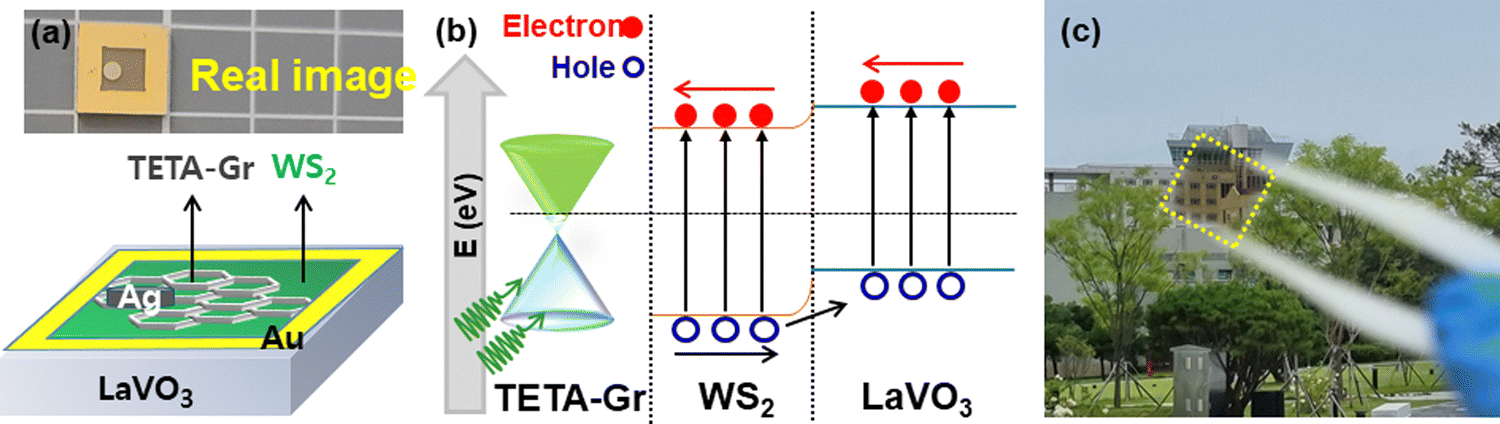 | ||
| Fig. 2 (a) Real image/schematic device structure and (b) its energy band structure. (c) Photograph of a TETA-Gr/WS2/LaVO3 device (yellow dotted line). This photo shows the semitransparency of the device. | ||
Fig. 3(a) shows the current density–voltage (J–V) behavior of devices for various t under AM 1.5G illumination with an intensity of 100 mW cm−2. From the J–V curve, we systematically analyzed the open-circuit voltage (Voc), short-circuit current density (Jsc), fill factor (FF), and power conversion efficiency (PCE) of the t-dependent devices, as summarized in Table 1. As shown in Fig. 3(a) and Table 1, the Voc of the device nearly remained unchanged from 0.45 V to 0.43 V with different t. Meanwhile, as t increases from 70 to 300 nm, LaVO3 enhances light absorption, resulting in a gradual enhancement of Jsc. However, at t ≥ 200 nm, Jsc does not increase significantly. As t increases, transfer resistance, charge accumulation, and transfer time improve, thereby reducing FF. However, the reduction of FF is largely offset by the increase in Jsc, resulting in higher efficiency for larger t. The ST solar cell exhibits the highest efficiency with 0.43 V Voc, 20.20 mA cm−2Jsc, 62.43% FF, and 5.42% PCE at t = 300 nm. As a control sample, pristine-Gr/WS2/LaVO3 cell displays efficiencies of 1.12–2.85% (Fig. S4a and Table S1, ESI†). The relatively low efficiency for pristine Gr-based ST cells is a result of the high sheet resistance of pristine Gr and the mismatch of the work function at the interface. Fig. 3(b) presents the external quantum efficiency (EQE) spectra from the wavelength of 300–1000 nm for t-dependent cells. As is well known, we calculated EQE from photo-harvesting efficiency, charge injection/transfer efficiency, and charge collection efficiency.36 Consequently, the EQE of TETA-Gr-based cells gradually improved over almost the entire wavelength range as t increased from 70 to 300 nm (Fig. 3(b)). Likewise, devices with pristine-Gr showed the same trend (Fig. S4b, ESI†). The deviation between the integrated Jsc evaluated from the EQE spectrum and Jsc measured at 1 sun was within 5%, as summarized in Table 1. This feature is due to the close correlation between Jsc and integrated EQE values.36,37
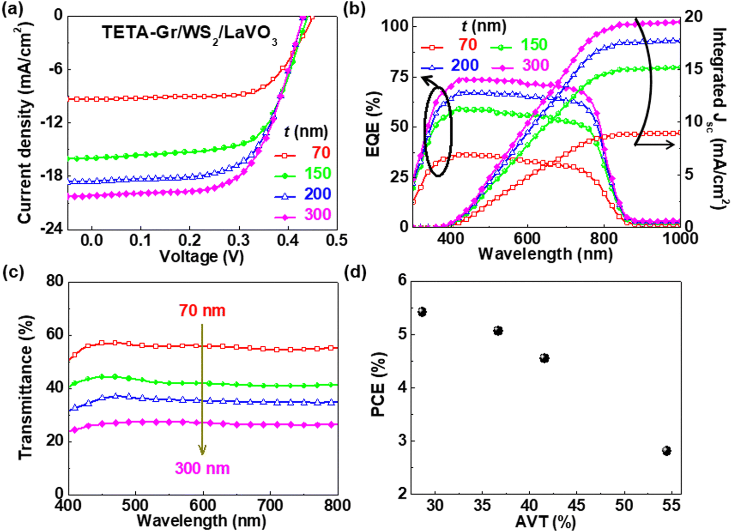 | ||
| Fig. 3 (a) Photo J–V curves and (b) EQE spectra/integrated Jsc of TETA-Gr/WS2/LaVO3 solar cells for various t. (c) Spectral transmittance of a typical semitransparent solar cell on quartz. (d) Dependence of the average efficiency on the average visible transmittance of the device. | ||
| t (nm) | V oc (V) | J sc (mA cm−2) | FF (%) | PCE (%) | Integrated Jsc (mA cm−2) | AVT (%) |
|---|---|---|---|---|---|---|
| 70 | 0.45 | 9.38 | 66.73 | 2.81 | 8.98 | 55 |
| 150 | 0.44 | 15.98 | 64.66 | 4.55 | 15.21 | 42 |
| 200 | 0.43 | 18.61 | 63.39 | 5.07 | 17.75 | 35 |
| 300 | 0.43 | 20.20 | 62.43 | 5.42 | 19.50 | 26 |
Fig. 3(c) shows the T spectrum of TETA-Gr/WS2/LaVO3 cells as a function of t. As the t of LaVO3 increases, the T for all wavelengths decreases due to the increase in light absorption. We evaluated the AVT associated with the wavelength of 400–800 nm range for all cells. As t increases from 70 to 300 nm, the AVT decreases from 55 to 26%, showing opposite trends. Fig. 3(d) plots the PCE versus AVT of the full cell. We observe clear trends such as: at the lowest 26% AVT, the PCE approaches 5.42% and decreases as the T increases. The efficiency of the most transparent cell with an AVT of 55% was about 2.81%. Considering the results of PCE and AVT, we believe that it is most suitable for ST solar cells at t = 200 nm. To maximize the benefits of the translucent solar cell properties, we measured the J–V behavior using an Al reflective mirror for t = 200 nm. Here, the Al mirror helps re-absorption of the device by reflecting the light in the UV-visible region, as shown in the schematic diagram of Fig. 4(a). In the system with Al mirrors, the efficiency of the device was 5.64%, an improvement of approximately 12% compared to the device without mirrors, as summarized in Table 2 (Fig. 4(b)).
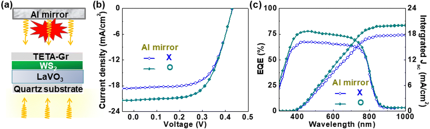 | ||
| Fig. 4 (a) Schematic diagram illustrating the measurement method of a semitransparent solar cell equipped with an Al reflective mirror. (b) J–V curves of the semitransparent cell for t = 200 nm without/with an Al reflective mirror. (c) EQE spectra of devices without/with Al mirror. | ||
| Light reflection | V oc (V) | J sc (mA cm−2) | FF (%) | PCE (%) |
|---|---|---|---|---|
| No mirror | 0.43 | 18.61 | 63.39 | 5.07 |
| With mirror | 0.43 | 21.40 | 61.03 | 5.64 |
Fig. 4(c) shows the EQE spectra of devices with/without Al mirrors. The integrated Jsc of both devices is 18.61 and 21.40 mA cm−2, respectively, suggesting improved EQE over a wide wavelength range of 350–800 nm compared to Al mirror-free based devices. This demonstrates a significant improvement in Jsc due to the increased light harvesting efficiency thanks to the Al mirror.
Finally, we measured the J–V properties under continuous 1 sun with 60 °C temperature (Ta)/30% relative-humidity (RH) and 80 °C Ta/50% RH to check the stability of the device including 5.02% PCE and 35% AVT. Fig. 5(a) shows the evolution of PCE during 1000 h under 1 sun. Fig. 5(b) and (c) shows the J–V curves of the device before and after continuous 1-sun illumination for two conditions. As a result, the devices changed slightly from 5.01% to 4.51 and 4.23% for 60 °C Ta/30% RH and 80 °C Ta/50% RH, respectively, maintaining 91 and 84% of the original PCE. The stability of TETA-Gr TCE was also monitored for sheet resistance under the same conditions (60 °C Ta/30% RH and 80 °C Ta/50% RH). The initial sheet resistance of TETA-Gr TCE before illumination was 208 ± 12 Ohm sq−1. After 1000 h, the sheet resistance increased by ∼1.07/1.15 times the initial value for 60 °C Ta/30% RH and 80 °C Ta/50% RH, respectively (Fig. S5, ESI†). This confirmed that cell deterioration can be mainly caused by an increase in sheet resistance of TETA-Gr, but the increase in sheet resistance is not significant, resulting in a small decrease in efficiency. It is believed that the source of this high stability comes from the excellent chemical and thermal stability of TETA-Gr, WS2, and LaVO3 materials, as reported in previous literature.21,28,38–40 These results demonstrate that TETA-Gr/WS2/LaVO3 ST solar cells are excellent in photo-stability.
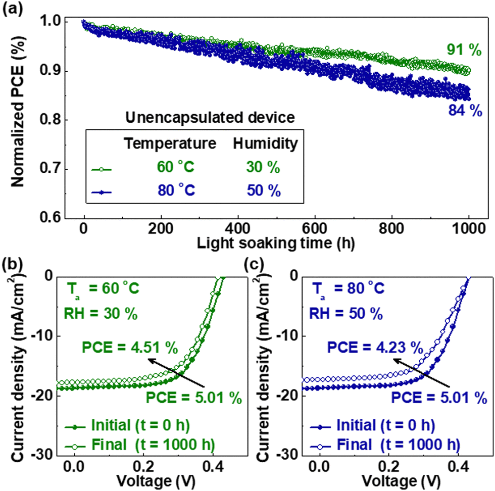 | ||
| Fig. 5 (a) Photo-stabilities of TETA-Gr/WS2/LaVO3 solar cells under continuous illumination of 1 Sun for 1000 h at 60 °C temperature (Ta)/30% relative-humidity (RH) and 80 °C Ta/50% RH. J–V curves of the solar cells for initial (t = 0 h) and final (t = 1000 h) under (b) 60 °C Ta/30% RH and (c) 80 °C Ta/50% RH. | ||
4. Conclusion
We have successfully demonstrated a novel ST solar cell using a translucent and photoactive LaVO3 layer and TETA-Gr TCE. With increasing t, the efficiency of the device increased from 2.66 to 5.42%, but the AVT decreased from 55 to 26%. A good ST solar cells must meet high efficiency and visual effects. Considering efficiency and AVT, translucent solar cells are considered to have the optimal condition at t = 200 nm. The PCE of the ST solar cell was improved by approximately 12% by adding an Al reflective mirror compared to a system without an Al mirror. Furthermore, the PCE of the TETA-Gr/WS2/LaVO3 device decreased by only 9 and 16% compared to the initial PCE even after 1000 h under 1 sun in an atmosphere of 60 °C Ta/30% RH and 80 °C Ta/50% RH, respectively, demonstrating thermal stability.Conflicts of interest
There are no conflicts to declare.Acknowledgements
This work was supported by the National Research Foundation of Korea (NRF) grant funded by the Ministry of Science, ICT & Future Planning: NRF-2021R1F1A1045446 (H. LEE) and NRF-2022R1C1C1008499 (D.H. SHIN).References
- M. H. Alsharif, J. Kim and J. H. Kim, Sustainability, 2018, 10, 1822 CrossRef.
- S. Kim, M. Patel, S.-M. Youn, Y. Kim, K. Lee and J. Kim, Mater. Today Energy, 2023, 31, 101203 CrossRef CAS.
- S.-H. Lim, H.-J. Seok, M.-J. Kwak, D.-H. Choi, S.-K. Kim, D.-H. Kim and H.-K. Kim, Nano Energy, 2021, 82, 105703 CrossRef CAS.
- S. Yoon, H. U. Ha, H.-J. Seok, H.-K. Kim and D.-W. Kang, Adv. Funct. Mater., 2022, 32, 2111760 CrossRef CAS.
- S. Lie, A. Bruno, L. H. Wong and L. Etgar, ACS Appl. Mater. Interfaces, 2022, 14, 11339–11349 CrossRef CAS PubMed.
- Y.-W. Zhang, P.-P. Cheng, W.-Y. Tan and Y. Min, Appl. Surf. Sci., 2021, 537, 147908 CrossRef CAS.
- G. Giuliano, A. Bonasera, G. Arrabito and B. Pignataro, Sol. RRL, 2021, 5, 2100702 CrossRef CAS.
- D. Wang, H. Liu, Y. Li, G. Zhou, L. Zhan, H. Zhu, X. Lu, H. Chen and C.-Z. Li, Joule, 2021, 5, 945–957 CrossRef CAS.
- G. P. Kini, S. J. Jeon and D. K. Moon, Adv. Funct. Mater., 2021, 31, 2007931 CrossRef CAS.
- X. Huang, L. Zhang, Y. Cheng, J. Oh, C. Li, B. Huang, L. Zhao, J. Deng, Y. Zhang, Z. Liu, F. Wu, X. Hu, C. Yang, L. Chen and Y. Chen, Adv. Funct. Mater., 2022, 32, 2108634 CrossRef CAS.
- J. Jing, S. Dong, K. Zhang, Z. Zhou, Q. Xue, Y. Song, Z. Du, M. Ren and F. Huang, Adv. Energy Mater., 2022, 12, 2200453 CrossRef CAS.
- Z. Hu, J. Wang, X. Ma, J. Gao, C. Xu, X. Wang, X. Zhang, Z. Wang and F. Zhang, J. Mater. Chem. A, 2021, 9, 6797–6804 RSC.
- T. A. Chowdhury, M. A. B. Zafar, M. S.-U. Islam, M. Shahinuzzaman, M. A. Islam and M. U. Khandaker, RSC Adv., 2023, 13, 1787–1810 RSC.
- H. H. Park, Nanomaterials, 2022, 12, 112 CrossRef CAS PubMed.
- L. A. Frolova, Q. Chang, S. Y. Luchkin, D. Zhao, A. F. Akbulatov, N. N. Dremova, A. V. Ivanov, E. E. M. Chia, K. J. Stevenson and P. A. Troshin, J. Mater. Chem. C, 2019, 7, 5314–5323 RSC.
- P. Jiang, L. Hu, L. Sun, Z. Li, H. Han and Y. Zhou, Chem. Sci., 2022, 13, 4714–4739 RSC.
- H. T. Zhang, M. Brahlek, X. Ji, S. Lei, J. Lapano, J. W. Freeland, V. Gopalan and R. Engel-Herbert, ACS Appl. Mater. Interfaces, 2017, 9, 12556–12562 CrossRef CAS PubMed.
- L. Wang, Y. Li, A. Bera, C. Ma, F. Jin, K. Yuan, W. Yin, A. David, W. Chen, W. Wu, W. Prellier, S. Wei and T. Wu, Phys. Rev. Appl., 2015, 3, 064015 CrossRef.
- M. Jellitea, J.-L. Rehspringerb, M. A. Fazioc, D. Mullera, G. Schmerberb, G. Ferblantiera, S. Colisb, A. Diniab, M. Sugiyamad, A. Slaouia, D. Cavalcolic and T. Fix, Sol. Energy, 2018, 162, 1–7 CrossRef.
- C. Sun, J. A. Alonso and J. Bian, Adv. Energy Mater., 2020, 11, 2000459 CrossRef.
- D. H. Jung, J. W. Hwang, J. J. Lee, D. H. Shin and H. Lee, J. Alloys Compd., 2022, 904, 163818 CrossRef CAS.
- J. J. Lee, D. H. Jung, D. H. Shin and H. Lee, Nanotechnology, 2022, 33, 395202 CrossRef PubMed.
- D. H. Shin, D. H. Jung and H. Lee, ACS Omega, 2023, 8, 18695–18701 CrossRef CAS PubMed.
- J. J. Lee, D. H. Shin, D. H. Jung, S. D. Oh and H. Lee, J. Alloys Compd., 2023, 937, 168404 CrossRef CAS.
- D. H. Shin, J. S. Ko, S. K. Kang and S.-H. Choi, ACS Appl. Mater. Interfaces, 2020, 12, 4586–4593 CrossRef CAS PubMed.
- J. M. Kim, S. Kim and S.-H. Choi, ACS Sustainable Chem. Eng., 2019, 7, 734–739 CrossRef CAS.
- D. H. Shin, C. W. Jang, H. S. Lee, S. W. Seo, S. Kim and S.-H. Choi, Appl. Surf. Sci., 2018, 433, 181–187 CrossRef CAS.
- I. Jo, Y. Kim, J. Moon, S. Park, J. S. Moon, W. B. Park, J. S. Lee and B. H. Hong, Phys. Chem. Chem. Phys., 2015, 17, 29492–29495 RSC.
- A. J. Watson, W. Lu, M. H. D. Guimãraes and M. Stöhr, 2D Mater., 2021, 8, 032001 CrossRef CAS.
- S. Riccardo, M. Elisabetta, A. Davide, N. Concetta, M. Rosanna, R. Simona, G. Cinzia, D. C. Pantaleo, R. Aurora and M. Cosimino, Nanomaterials, 2021, 11, 1969 CrossRef PubMed.
- Y. Li, X. Li, T. Yu, G. Yang, H. Chen, C. Zhang, Q. Feng, J. Ma, W. Liu, H. Xu, Y. Liu and X. Liu, Nanotechnology, 2018, 29, 124001 CrossRef PubMed.
- W. Zhao, Z. Ghorannevis, K. K. Amara, J. R. Pang, M. Toh, X. Zhang, C. Kloc, P. H. Tane and G. Eda, Nanoscale, 2013, 5, 9677–9683 RSC.
- Y. Kim, J. Ryu, M. Park, E. S. Kim, J. M. Yoo, J. Park, J. H. Kang and B. H. Hong, ACS Nano, 2014, 8, 868–874 CrossRef CAS PubMed.
- X. Dong, D. Fu, W. Fang, Y. Shi, P. Chen and L.-J. Li, Small, 2009, 5, 1422–1426 CrossRef CAS PubMed.
- S. De and J. N. Coleman, ACS Nano, 2010, 4, 2713–2720 CrossRef CAS PubMed.
- J. D. Servaites, M. A. Ratner and T. J. Marks, Appl. Phys. Lett., 2009, 95, 163302 CrossRef.
- M. Saliba, E. Unger, L. Etgar, J. Luo and T. J. Jacobsson, Nat. Commun., 2023, 14, 5445 CrossRef CAS PubMed.
- Y. Liua, W. Huang, W. Chen, X. Wang, J. Guo, H. Tian, H. Zhang, Y. Wang, B. Yu, T.-L. Ren and J. Xu, Appl. Surf. Sci., 2019, 481, 1127–1132 CrossRef.
- J. D. Yao, Z. Q. Zheng, J. M. Shao and G. W. Yang, Nanoscale, 2015, 7, 14974–14981 RSC.
- S. Pace, M. Ferrera, D. Convertino, G. Piccinini, M. Magnozzi, N. Mishra, S. Forti1, F. Bisio, M. Canepa, F. Fabbri and C. Coletti, J. Phys. Mater., 2021, 4, 024002 CrossRef CAS.
Footnotes |
| † Electronic supplementary information (ESI) available. See DOI: https://doi.org/10.1039/d3tc03411a |
| ‡ These two authors have contributed equally to this study. |
| This journal is © The Royal Society of Chemistry 2024 |