
 Open Access Article
 This Open Access Article is licensed under a
 Creative Commons Attribution 3.0 Unported Licence
On-surface growth of transition-metal cobalt nanoclusters using a 2D crown-ether array†
Toyo Kazu
Yamada
 *ab,
Ryohei
Nemoto
a,
Fumi
Nishino
a,
Takuya
Hosokai
c,
Chi-Hsien
Wang
d,
Masaki
Horie
d,
Yuri
Hasegawa
e,
Satoshi
Kera
e and
Peter
Krüger
ab
*ab,
Ryohei
Nemoto
a,
Fumi
Nishino
a,
Takuya
Hosokai
c,
Chi-Hsien
Wang
d,
Masaki
Horie
d,
Yuri
Hasegawa
e,
Satoshi
Kera
e and
Peter
Krüger
ab
aDepartment of Materials Science, Chiba University, 1-33 Yayoi-Cho, Inage-ku, Chiba 263-8522, Japan. E-mail: toyoyamada@faculty.chiba-u.jp
bMolecular Chirality Research Centre, Chiba University, 1-33 Yayoi-cho, Inage-ku, Chiba 263-8522, Japan
cNational Metrology Institute of Japan, National Institute of Advanced Industrial Science and Technology, Tsukuba Central 5, 1-1-1, Higashi, Tsukuba, Ibaraki 305-8565, Japan
dDepartment of Chemical Engineering, National Tsing Hua University, 101, Sec. 2, Kuang-Fu Road, Hsinchu, 30013, Taiwan
eInstitute for Molecular Science, Myodaiji, Okazaki 444-8585, Japan
First published on 11th December 2023
Abstract
Advanced methods of producing nanometer-size transition metal clusters have enhanced the functionality of nanoclusters (NCs), leading to single-atom catalysis, miniaturization of spintronics media, and biomedicine. Herein, on-surface growth of transition-metal cobalt (Co) NCs in a vacuum was demonstrated using a structurally flexible two-dimensional (2D) 4,4′,5,5′-tetrabromodibenzo[18]crown-6 ether (BrCR) ring molecular array, prepared on an atomically flat noble metal Cu(111) surface. Then, we successfully produced two different sizes (∼1.5 nm and ∼3.6 nm) of Co NCs using the trapping ability of BrCR. The growth and electronic structures of Co NCs were investigated by low-temperature scanning tunneling microscopy/spectroscopy (STM/STS) and angle-resolved photoelectron spectroscopy (ARPES) in an ultrahigh vacuum. DFT calculations unveiled the energetically stable adsorption sites. The growth process of Co NCs is governed by the electronic π–d hybridization between BrCR and Co. Once the Co atom was trapped, it became a nucleation center, around which other Co atoms gathered to form a nanocluster. In contrast to the standard behavior of crown ether molecules in solution, the stable position of the trapped metal atom is not at the center of the crown ring but at the BrCR edge, where the Co atom is located below the side substituents.
1. Introduction
Transition-metal nanoclusters (NCs) using 3d metals, e.g., Co, Ni, CoPt, FePt, Fe3O4, and Fe2O3, with a size of 10–100 nm coated by chemical compounds have drastically advanced in a wide variety of promising applications such as biomedicine,1,2 drug delivery,3,4 catalysts,5–7 and water purification.8 Downsizing the cluster to a few nanometers or atomic size has encouraged further functionality such as single-atom catalysis9,10 or miniaturization of spintronics media.11,12 For that, the coordination of organic molecules with transition-metal atoms could be an essential key factor. Since π-conjugated molecules, e.g., phthalocyanines (Pc) or tetraphenyl porphyrins (TPP), have a size of about 1 nm, the metalation of self-assembled monolayer (SAM) molecular films on 2D surfaces could be a novel method to promote the downsizing of the nanocluster.13–15 However, the SAM films can trap only one atom per molecule. Suppose the number of adsorbed transition metal atoms exceeds the number of molecules. In that case, the SAM orderliness is broken, and other atoms grow independently from the molecules, leading to a messy surface.16In this study, we demonstrated the adsorption of the “guest” 3d transition-metal cobalt (Co) on the “host” well-ordered ring molecular array at room temperature in ultra-high vacuum (UHV). Crown ether molecules in 4,4′,5,5′-tetrabromodibenzo[18]crown-6 ether (BrCR) SAM films were used as a “host,” which have been studied since the 1960s as cyclic molecules with an intramolecular ring in bulk crystal and liquid solution.17–23 This kind of ring is well-known as a host, i.e., a molecule that can trap guest metal atoms, molecules, or ions. Because of the flexibility of the O–C–O bond angles, the crown ring is easily deformed, and BrCR has different bent conformations in the gas phase and the bulk crystal. However, it was recently shown that the crown ring can be unfolded when BrCR forms a self-assembled monolayer (SAM) ring array on a metal Cu(111) surface.24 Herein, Co was selected as the “guest” since the growth, electronic, and magnetic structures of bilayer triangular-shape Co nanoislands on Cu(111) substrate are well known.25–28 Although there are reports on the adsorption of Co ions on crown ether molecules in bulk,29 no studies have been conducted on crown ether and metal clathrate compounds on solid surfaces in a vacuum.
Here, we demonstrate that two sizes of equivalent-sized Co NCs can be produced on 2D surfaces using the trapping ability of BrCR, and the growth process was elucidated using complementary techniques of both experimental and theoretical simulations, such as a home-built low-temperature (78 K) UHV scanning tunneling microscopy/spectroscopy (STM/STS) setup, a UHV angle-resolved photoelectron spectroscopy (ARPES) setup with low energy electron diffraction (LEED), and density functional theory (DFT) calculation.
2. Experimental section
A home-built STM setup combined with the Nanonis SPM controller BP4 (ESI†) was used to obtain topographic images of sample surfaces in a constant current mode. All STM results were obtained at 78 K in UHV. We used sharp tungsten tips as STM probe tips.30–32 ARPES and LEED measurements were conducted in the home-built UHV apparatus (Supplementary Notes, ESI†).2.1 STM/STS measurements
Since the tunneling current (I) detected by the tip is exponentially proportional to the tip-sample separation (z) via exp(−(8m (Φ ± eV/2))1/2z/ℏ), where m: electron mass, ℏ: Planck constant, Φ: apparent barrier height between tip and sample, and V: set point sample bias voltage,33–35 STM can measure the surface corrugations in the order of 1 pm. STS measures the sample surface local density of states (LDOS). Tunneling current, I, as a function of sample bias voltages (typically, from −2 V to +2 V), was measured under a feedback off condition (one single curve was measured within 50–200 ms) by fixing the tip-sample separation (z = zc), which was determined by the setpoint voltage (Vs) and the current (Is). The obtained I(V) curves were numerically differentiated, and differential conductance (dI/dV) curves were obtained, which were proportional to LDOS. In the dI/dV curve, positive and negative bias voltages mean unoccupied and occupied LDOS, respectively. Zero eV corresponds to the Fermi energy. The STM/STS data were analyzed using WSxM 5.0 Develop 10.2 software,36 and Gwyddion 2.53.2.2 Cu(111) cleaning process
We used two Cu(111) single crystals, one for ARPES/LEED and another for STM. Both Cu(111) single crystals (diameter 6 mm, MatecK, 99.999%) were carefully sputtered and annealed to obtain clean and atomically flat surfaces in the preparation chambers (<5.0 × 10⁻⁸ Pa). Cleaning parameters were Ar+ sputtering (+1.0 keV, 0.4 μA) and annealing (∼820 K) for the STM setup, and Ar+ sputtering (+0.6 keV, 3.0 μA) and annealing (∼770 K) for the ARPES setup. The Cu(111) was cleaned using a conventional way of repeating Ar+ sputtering and annealing in the preparation chamber, and Co was deposited on Cu(111) in the same chamber.2.3 Characterization of the synthesized BrCR
Characterization data of the used BrCR molecules are summarized as follows: 1H NMR (500 MHz, CDCl3, r.t.): δH 3.94 (t, 8H, OCH2, J(HH) = 5 Hz), 4.09 (t, 8H, OCH2, J(HH) = 5 Hz), 7.01 (s, 4H, C6H2(catechol)) (Fig. S1, ESI†). HRFDMS calcd. For C20H20Br4O6 [M]+ (m/z): 671.79989, found: 671.80053 (error 0.96 ppm) (Fig. S2, ESI†). CCDC 1901496 contains supplementary crystallographic data (Fig. S3, ESI†).2.4 BrCR molecule evaporation in UHV
BrCR molecules were deposited in the deposition chamber (<3.0 × 10⁻⁷ Pa) with sublimation rate control using a quartz crystal microbalance (QCM).37 We used two different UHV setups: one for ARUPS and LEED and another one for low-temperature STM. Therefore, it was necessary to control precisely the amount of deposited molecules on the Cu(111) substrate at 300 K in both setups. We used the quartz SiO2 crucible and homebuilt molecular evaporator (thermal radiation heating) to obtain the same crucible temperature and pressure (1 × 10⁻⁶ Pa). For the QCM calibration for checking the sublimation rate, parameters were set to z-ratio = 1, density = 1. The quarts crucible was radiatively heated by flowing current through a tungsten wire filament (diameter 0.3 mm). The crucible temperature was monitored using the alumel-chromel thermocouple contacting the bottom of the crucible. The Cu(111) substrate was put ∼110 mm above the crucible. Before the deposition, we always checked the BrCR evaporation rate by setting a QCM at the same distance position. We carefully increased the crucible temperature in time, and precisely above the crucible temperature of 357 K, and QCM detected the molecule deposition. The evaporation speeds of 0.03 nm min−1 and 0.08 nm min−1 were reproducibly obtained at the crucible temperature of ∼361 K and ∼369 K, respectively. Since the QCM parameters of z-ratio and molecule density, the estimated deposition amounts, and the adsorption probability on the substrate were unknown, the molecule thickness estimated by QCM was only used as an index. STM checked the precise deposited molecular monolayer (ML).2.5 Cobalt deposition in UHV
Co atoms were deposited from an electron bombardment type evaporator (AEV-3, AVC Co., Ltd) at a sample temperature of 300 K in UHV. Hot electrons from a W wire ring located above a Co rod (diameter 2.0 mm, purity 99.99%) were accelerated by ∼800 eV to the apex, which melted and evaporated only the apex of the Co rod, leading to a Co evaporation flux of about 5 nA. The deposition amounts of Co were controlled from STM topographic images of Co island growth on Cu(111).2.6 DFT calculation
Density functional theory calculations were performed with the projector augmented wave method as implemented in the VASP code.38,39 The numerical settings were the same as in our previous study on BrCR/Cu(111).24 We used the PBE exchange–correlation potential and Grimme's DFT-D2 van der Waals correction, where the C6 parameter of Cu was rescaled by 50%.This scaling parameter was determined through test calculations on benzene/Cu(111), in order to correct overbinding between benzene-type pi-orbital and metal surfaces within DFT-D2.24 More recent dispersion correction schemes, such as DFT-D3, have been found to be superior to D2 for metals40,41 and should give reliable results without the need for parameter rescaling. Nonetheless, here we chose to keep the same computational settings as in our previous work24 for consistency and easy comparison.
A plane-wave energy cut-off of 400 eV and a 2 × 4 × 1 k-point grid for the Cu(111) 7 × 4 supercell were used. The Cu(111) substrate was modeled with four atomic layers. Starting from the stable structure of BrCR/Cu(111), one Co atom was put at various initial positions in the proximity of the molecule. Then, all atomic positions, except those in the two lowest Cu layers, were optimized until the forces were less than 0.2 eV per atom.
3. Results and discussion
3.1 STM imaging of Co/Cu(111) and BrCR adsorption
The nanocluster (NC) formation using the transition metal cobalt (Co) and BrCR ring molecules is governed by two interactions between Co and BrCR and Co and the Cu substrate. To clarify the substrate interaction effect, we first checked the growth of Co on Cu(111). Then, we tested BrCR molecules adsorption on the Co nanoislands.Fig. 1(a) shows STM topographic images acquired on the pristine Cu(111) terraces, where triangular-shaped Co bilayer islands grew after the Co deposition. Here, the adsorbed Co atoms are thermally diffused on the Cu(111) terraces and form ordered structures following the fcc(111) symmetry.
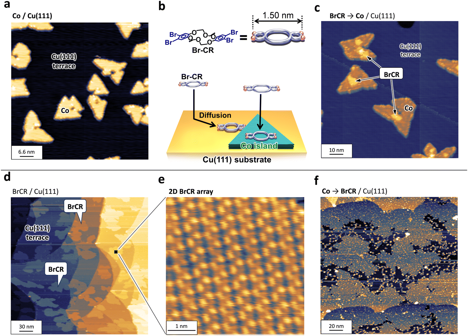 | ||
| Fig. 1 (a) STM topographic image of Co bilayer nanoislands on Cu(111) (66 × 66 nm2, −1 V, 87 pA). (b) BrCR molecule adsorption model on these Co islands. (c) STM topographic image of Co nanoislands on Cu(111) after the BrCR deposition (100 × 100 nm2, −1 V, 10 pA). (d) and (e) STM topographic images obtained on the surfaces of BrCR islands on Cu(111): (d) 300 × 300 nm2, −2 V, 10 pA and (e) the ordered BrCR array structure (5 × 5 nm2, −1.4 V, 10 pA). (f) STM topographic image obtained on the surface of Co islands on Cu(111) after the BrCR deposition (200 × 200 nm2, −2 V, 10 pA). | ||
Next, we demonstrated the interaction balance between Co and BrCR and between Cu and BrCR. If the Cu–BrCR interaction is stronger than the Co–BrCR interaction, BrCR and Co islands could grow separately and not interact. Here, we deposited BrCR molecules on the Co bilayer islands as depicted in the model in Fig. 1(b). Fig. 1(c) shows the result. Interestingly, we observed no BrCR islands. In contrast, new protrusions appear on the top and edge of the Co islands while the islands remain triangular. Namely, most adsorbed BrCR islands preferentially contact the Co islands. This means that the Co–BrCR interaction is stronger than the Cu–BrCR interaction. This experimental evidence in Fig. 1(c) further provides an idea of producing nanoclusters (NCs) by depositing Co atoms on the BrCR array.
3.2 Co-adsorption on BrCR 2D array
To adsorb Co atoms on the 2D BrCR array to create transition metal NCs, we first prepared the BrCR 2D array.17Fig. 1(d) shows BrCR array self-assembled monolayer (SAM) islands on Cu(111). The magnified image in Fig. 1(e) shows periodic ordered patterns on the BrCR islands, corresponding to the (7 × 4) superstructure.24About 0.01 cobalt monolayers (MLs) were deposited on the BrCR array at 300 K, and subsequently, STM/STS measurements were performed at 78 K without breaking UHV. Here, the ratio of the guest Co atoms to the host BrCR ring molecules was tuned to about two to nine (Fig. 2(a)). Fig. 1(f) represents an STM topographic image of the BrCR array islands after the Co deposition, where the observation clearly changed. Many bright spots appeared, indicating the Co NC formation instead of forming the triangular Co islands on Cu(111) depicted in Fig. 1(a). This suggests that the BrCR molecule trapped the adsorbed Co atoms, restringing their thermal diffusion and could form the metal–organic NCs. Also, bright spots were located at random positions, and the BrCR array lattice was maintained. This means trapped Co atoms could not be moved or intercalated even at 300 K. Namely, the Co–BrCR NC formation could be energetically stable owing to the strong Co–BrCR bonding.
 | ||
| Fig. 2 (a) Schematic model of Co atom deposition on the BrCR ordered array. (b) and (c) STM topographic images of Co nanoclusters (NCs) on the BrCR array: (b) 10 × 5 nm2 and (c) 10 × 10 nm2, −2 V, 10 pA. The inset in (b) denotes height profiles crossing five different NCs. (d) STS results obtained on the Co NCs. The left panels denote simultaneous obtained topographic image (20 × 7 nm2, −2.5 V, 200 pA) and dI/dV maps at −1.5 V and +1.5 V. The right panel denotes dI/dV curves obtained on the NCs (blue, red, and grey dots) and the BrCR array (green dots). | ||
Fig. 2(b) shows a magnified STM topographic image inside one BrCR domain after Co deposition. The white lines in Fig. 2(b) denote the BrCR lattice. Here, NCs observed as bright spots are kept within the BrCR 2D array. Height profiles crossing randomly selected five different NCs as depicted in the inset in Fig. 2(b) indicating that the NCs have rather uniform size, namely ∼200 pm height and ∼1.5 nm diameter. Still, they are not the same shape, indicating different orientations and/or coordination of Co–BrCR NC structures because of the flexibility of the crown ether ring. Another indication of BrCR deformation can be explored by observing the darker area next to the spot, which could be peeled off the BrCR from the Cu(111) surface during the NC formation. Because the NC size is comparable to the one-unit cell size of the BrCR lattice, one-by-one trapping of the Co atom by the BrCR could occur.
Fig. 2(c) shows an STM topographic image of another BrCR domain, in which white dotted lines indicate the remaining unit cell of the BrCR lattice, and the intersection indicates the center position of the crown ring. BrCR molecule models are also shown in Fig. 2(c) as a guide to the eye. A one-unit cell contains one BrCR molecule. By comparing the BrCR lattice and the NC position, it is clear that the NCs do not grow at the center of the crown ether ring but are close to the intermolecular position.
We could estimate the number of Co atoms consisting of one NC. In the area shown in Fig. 2(c), the 0.01 MLs Co/Cu(111) corresponds to about 18 Co atoms deposited on about 136 BrCR molecules, while we could observe only eight NCs. This means that a single NC contains, on average, 18/8 ≥ 2 Co atoms. So, the NC includes not only one but more than two atoms. This is the clear difference compared to the previously studied π-conjugated Pc/TPP molecules, where only one atom can be trapped at the core, but extra Co atoms diffused and disordered the SAM film.16 In this sense, it is remarkable that the molecules surrounding the NC kept the original (7 × 4) superstructure, as shown by the white box in Fig. 2(c), including 5 by 3 BrCR molecules without disordering or deformation. Since a Co atom adsorbed and started to diffuse on the BrCR array surface, if the bonding between BrCR and Co is too strong, the Co atom should not move. However, the experimental results showed that one NC has more than two Co atoms. This growth can occur due to two Co atoms diffusing and meeting each other on the surface. Namely, the results in Fig. 2(c) indicate a low trapping ability of the Co atom by the crown ether ring in BrCR but suggest that once a Co atom was trapped, other diffusing Co atoms gathered, forming a nanocluster.
3.3 Electronic structures of Co–BrCR nanoclusters
The metal–organic NC formation process was also directly imaged in the electronic structures. As suggested in Fig. 1, the formation of Co–BrCR NCs is energetically more stable than the co-existence of isolated Co atoms and BrCR molecules. Namely, the 3d Co atom prefers to couple with BrCR molecules and could form a bonding state via π–d hybridization.We used scanning tunneling spectroscopy (STS) to measure the sample local density of states (LDOS) at each pixel position.33–35Fig. 2(d) shows, from top to bottom, an STM topographic image and dI/dV maps at −1.5 eV and +1.5 eV obtained on the same BrCR surface after the Co deposition, where two NCs exist.
Since the BrCR array has HOMO and LUMO peaks around −1.5 eV and +1.5 eV, which was checked from the dI/dV curve obtained on the pristine BrCR film on Cu(111) (see the ESI,† Fig. S8), the dI/dV maps obtained at −1.5 V and +1.5 V (left panels in Fig. 2(d)), whose brightness corresponds to the LDOS intensity, clearly showed the BrCR ordered pattern. This also means that the orderliness of the BrCR array in the electronic structure was preserved even after the Co nanocluster formation. Namely, the Co NC formation did not drastically change the overall surface electronic structure, but it changed only the local electronic structure around the Co NC. Because of the different contrast between the BrCR and Co NCs, NCs could have different LDOS from the BrCR.
We checked dI/dV curves obtained from the Co NCs, which were found to be classified into three types named α (67%, red line), β (22%, blue line), and γ (11%, grey line) as depicted in the right panel in Fig. 2(d). The green line denotes the dI/dV curve obtained on the BrCR array.
Interestingly, all dI/dV curves reveal peaks/shoulders at −0.73 and +0.25 eV despite the non-uniform topology of the NCs. The difference in the dI/dV might occur because of the non-flat surface of the NCs, which changes the local barrier height (Φ) of each nanocluster and varies the exponential background in the dI/dV curves,34 namely, dI/dV ∼ ρs(−(8m(Φ ± eV/2))1/2z/ℏ), where ρs denotes the sample LDOS, m is the electron mass, and z is the tip-sample separation. This means that the type α NCs (red line in Fig. 2(d)) have a lower local barrier height compared to the type β and γ NCs, increasing the background. The obtained LDOS features at −0.73 and +0.25 eV could indicate Co–BrCR bonding and antibonding states, respectively.
Another point to be noted is that the LDOS of the remaining BrCR-ordered molecular array is still preserved after the Co deposition. Only the LDOS of limited BrCR areas near the NCs were disturbed. These areas are encircled by a black line in the dI/dV maps in Fig. 2(d). The STM topographic image in Fig. 2(d) shows that the BrCR array of these areas is disordered. This could be a trace from when the NC formation pulled the BrCR from the 2D array.
3.4 Initial growth processes in nanocluster formation
Fig. 3(a)–(c) represents that the NCs located at the edge of the BrCR array could grow twice as fast. Fig. 3(a) and (b) show an STM topographic image and a current map obtained in the same area. Here, the latter visualized atom and molecule patterns. Height profiles along the blue and red arrows in Fig. 3(a) represent ∼200 pm and ∼400 pm in height and ∼1.5 nm and ∼2.0 nm in width, respectively (see Fig. 3(c)). The current map in Fig. 3(b) denotes the BrCR unit cell lattice, indicating the edge NC has a size of about two BrCR unit cells. Since Br atoms are located at the BrCR island's edges instead of the crown rings, these observations in Fig. 3(a)–(c) indicate a higher trapping ability by the edge instead of the crown ring.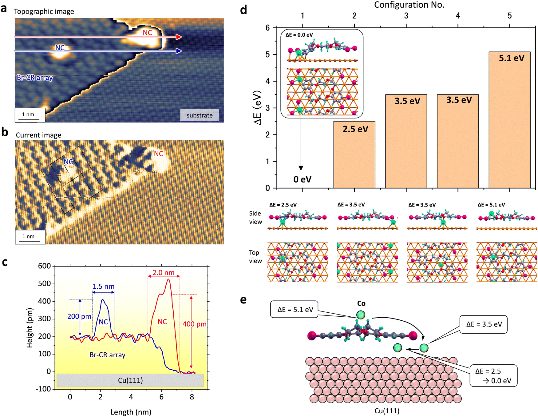 | ||
| Fig. 3 (a) and (b) Simultaneously obtained STM topographic image and current map at the edge of the BrCR array island, where two Co nanoclusters (NCs) are observed (10 × 5 nm2, −2 V, 10 pA). (c) Height profiles along the red and blue arrows in (a). (d) DFT calculation results of Co atom adsorption into the BrCR/Cu(111) system. Ball-and-stick models of five configurations are shown with Co, Br, O, C, H, and Cu atoms in green, magenta, red, grey, blue, and golden, respectively. Side and top views are shown. The Co atom is placed between Br atoms and the benzene ring (no. 1), below the benzene ring (no. 2), below or outside the Br atoms (no. 3), below the crown ring (no. 4), and above the benzene ring (no. 5). ΔE denotes the energy value difference from the most stable configuration. (e) DFT calculation suggested a model of how the adsorbed Co atom moved to the stable position. | ||
To clarify the mechanism of each growing mode, density functional theory (DFT) calculations were performed with the projector-augmented wave method implemented in the VASP code.38,39 The calculated DFT results shown in Fig. 3(d) shed further light on the growth processes of Co–BrCR NCs. First, the energetically stable configuration of the (7 × 4) BrCR superlattice on Cu(111) was calculated. Then, one Co atom was added to the BrCR lattice unit cell, and the adsorption energy (E) was calculated. Five configurations shown in Fig. 3(d) were examined to determine the energetically most stable configuration. Ball-and-stick models of five configurations are shown with Co, Br, O, C, H, and Cu atoms in green, magenta, red, grey, blue, and golden, respectively. Hexagonal lines denote the substrate fcc-Cu(111) lattice. The most energetically stable configuration among them was the Co atom placed between the benzene ring and bromine atoms, where the C–Br bond was broken, and a new C–Co–Br bond was formed. We indicate the structural energy (ΔE) relative to this structure (which has ΔE = 0.0 eV). The other configurations shown in Fig. 3(d) have higher energies of ΔE = 2.5 eV, 3.5 eV, 3.5 eV, and 5.1 eV, respectively. The second stable configuration was the Co atom located below the benzene ring. Although we expected intercalation of the Co atom below the BrCR molecules, the Co atom below the Br atoms (+3.5 eV) and the crown ring (+3.5 eV) revealed much higher energy. The most unstable position was the Co atom located on the BrCR molecule (+5.1 eV); this definitely rules out the possibility of Co atom adsorption on top of the BrCR molecules. These might indicate a similar behavior to the bulk crystal of Co(H2O6) in CR.29
Fig. 3(e) shows a schematic image of possible Co atom adsorption processes when a Co atom adsorbs on the center crown ring. First, the Co atom cannot stay on the molecule (+5.1 eV). Thus, the Co atom may intercalate below the crown ring. However, the position below the crown ring is still unstable (+3.5 eV). Hence, the Co atom starts to diffuse and moves to the side of the molecule, around the benzene ring (+2.5 eV), and could be trapped by the formation of the C–Co–Br bond (ΔE = 0.0 eV). These DFT results suggest the onset of the nanocluster growth.
3.5 Mass production of transition-metal nanoclusters
Finally, we evaluated how the on-surface method using a 2D BrCR array could produce plenty of equivalent-sized NCs. Fig. 4 shows experimental results. Fig. 4(a) and (b) demonstrate two different cases of Co adsorption on the BrCR array. The BrCR covered 75% of the former surface, but the latter surface was covered by only 15%. Then, it is found that Co NCs located on the Cu(111) terrace, apart from the BrCR array, have a larger size. Fig. 4(c) summarizes the diameter of NCs located inside the BrCR array. We checked the diameter of hundreds of the Co NCs. Then, we classified the sizes into 1.0, 1.5, and 2.0 nm for the smaller NCs, and 3, 4, and 5 nm for the larger NCs, which are shown in Fig. 4(c). Gaussian fittings to these distributions led to the average value of 1.5 ± 0.5 nm for the smaller-size NCs and 3.6 ± 1.2 nm for the larger-size NCs.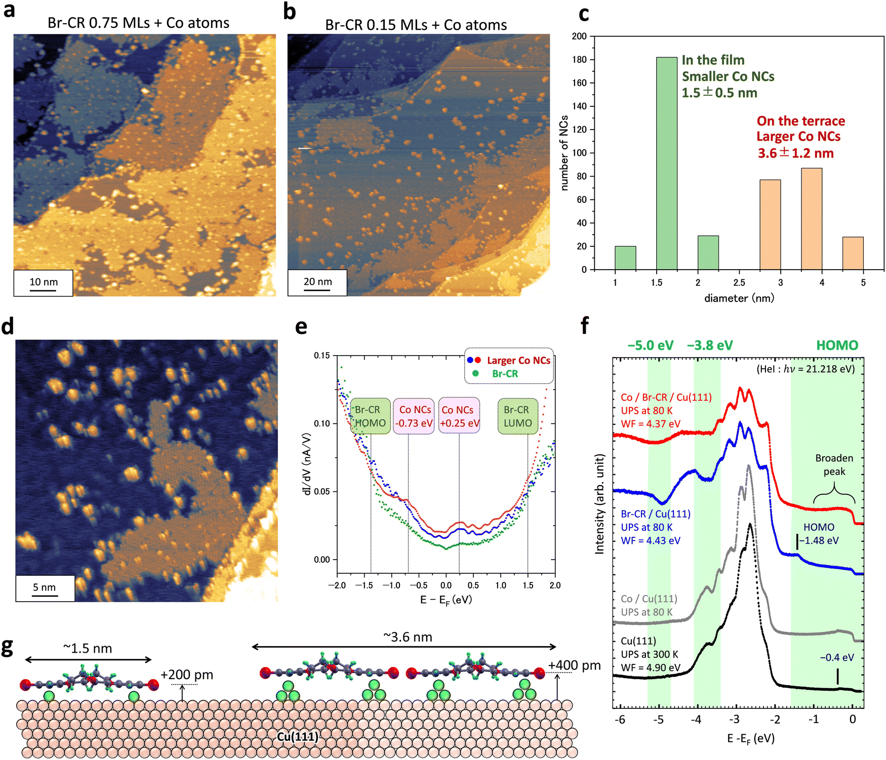 | ||
| Fig. 4 Co nanocluster formation on BrCR/Cu(111). (a) and (b) STM topographic images of Co atom adsorption on (a) 0.75 monolayers (MLs) and (b) 0.15 MLs of BrCR on Cu(111) (100 × 100 nm2, −2 V, 10 pA). (c) Nanocluster diameter histogram, indicating two different sizes of nanoclusters (NCs). (d) STM topographic image of Co NCs (50 × 50 nm2, −2 V, 10 pA). (e) dI/dV curves obtained on the larger-size Co NCs (blue and red dots) and BrCR array (green dots). (f) PES spectra obtained from the surfaces of the bare Cu(111) surface (black line), 0.57 MLs Co/Cu(111) (grey line), 1.0 ML BrCR film on Cu(111) (blue line), and 0.57 MLs Co film on the 1.0 ML Br-CR film/Cu(111) (red line). These PES spectra were measured in the Γ–K direction in the Brillouin zone of the Cu(111) surface and summed up from 0.0 to 1.1 Å−1. Experimentally obtained work function (WF) values are also shown. (g) Schematic model of two types of NCs. | ||
In Fig. 4, it is essential to know that many NCs were isolated on the Cu terrace. This indicates a necessary message that the isolated NCs could be energetically stable. First, the absorbed Co atom was trapped by the BrCR array's edges, similar to Fig. 3(a). Second, other Co atoms gathered, and the NC's size increased. The NC could be released when the NC thermal fluctuation overcame the bonding with the BrCR array. Repeating the drawing out of BrCR from the array and isolating NC formation made the array shrink and disarrange the array edges.
Fig. 4(e) shows dI/dV curves obtained on the larger-size (∼3.6 nm) isolated NCs, whose energy positions are identical to the initial growth of the smaller-size (∼1.5 nm) NCs in Fig. 2(d). Increasing the amount of the Co atoms inside BrCR could lead to enhanced charge transfer. However, both small (∼1.5 nm in Fig. 2(d)) and large (∼3.6 nm in Fig. 4(e)) Co NCs have similar dI/dV curves with LDOS peaks around −0.73 and +0.25 eV. No significant change was observed, suggesting that the charge transfer effect is rather small.
While STS measures the sample surface LDOS with high spatial resolution in the vicinity of the Fermi energy for both occupied and unoccupied states, angle-resolved photoemission spectroscopy (ARPES) measures the occupied DOS of a large surface area, detecting macroscopic surface and interface electronic structures. Here, averaging information of the mass-produced NCs was further investigated.
Fig. 4(f) shows the PES spectra obtained on the bare Cu(111) (black line), 0.57 MLs Co/Cu(111) (grey line), and 1 ML BrCR film on Cu(111) before (blue line) and after (red line) the 0.57 MLs Co deposition. The PES intensity curves were obtained by summing up ARPES data from 0.0 to 1.1 Å−1 along the Γ–K direction in the Brillouin zone (see the ESI,† Fig. S4 and S5). The binding energy at zero eV denotes the Fermi energy. The Cu(111) has a surface state at −0.4 eV (a small peak in the spectrum) and 3d band peaks between −2.5 and −4.5 eV with a work function (WF) of 4.90 eV. When the Cu(111) surface was covered with the 1 ML BrCR film, the work function was lowered to 4.43 eV due to the interface dipole induced by a molecular permanent dipole and charge transfer at the interface. The Cu surface state peak disappeared, and a HOMO peak at −1.48 eV appeared, which corresponds to the energy position of the HOMO peak measured by STS.24 Also, the spectrum peak shape changes to two-dip and one-peak features after the 3d band region around −3.8 eV, indicating the superposition of molecular orbital features.
We deposited 0.57 MLs Co on the BrCR film. The red spectrum shows that the BrCR HOMO peak at −1.48 eV is strongly quenched. This could indicate the disordering of the BrCR ordered array, and the BrCR nanocluster formation would give a broadened feature of HOMO-derived states. On the other hand, the intensity between −1 eV and 0 eV increased compared to the blue spectrum obtained on the bare BrCR (see the red spectrum in Fig. 4(f)), which could have the exact origin as the LDOS peak at −0.73 eV in the STS curve. The PES spectra difference between before and after Co deposition is also shown in the ESI,† Fig. S4. A similar intensity increase was observed on the Co/Cu(111) surface (grey line), indicating a shoulder near the Fermi energy (around −0.2 eV). In contrast, the band peaks between −2.0 eV and −3.5 eV show no difference before and after the Co deposition, mainly dominated by the Cu 3d state.42 Unfortunately, it is not easy to give any information on the spectral difference from types of Co NCs with the present experimental conditions. The dips at −3.8 eV and −5 eV became flat, which could be due to the shift and broadening behavior of deeper-lying orbital states as found for the HOMO, interacting weakly among the 3d Co states and the substrate Cu 3d states.
LEED spot patterns of the 2D BrCR array wholly disappeared after the Co deposition (ESI,† Fig. S6), in agreement with the mass-productive NCs on Cu(111) (see also the complete NC formation on the surface in the ESI,† Fig. S7).
Finally, a growth model of the two types of NCs is shown in Fig. 4(g). The smaller 1.5 nm size NCs, whose size is comparable to one BrCR molecule, could consist of one BrCR including more than two Co atoms below the BrCR, increasing the height of +200 pm. The larger 3.6 nm size NCs seem to include more than two BrCR molecules, and the Co bilayer likely grew below molecules since the height increase is comparable to the Co bilayer height (∼400 pm) in Fig. 1(a). This suggests the larger NC includes more than 10 Co atoms.
4. Conclusions
We demonstrated the growth of transition-metal cobalt (Co) nanoclusters (NCs) using the trapping ability of the 2D crown-ether (BrCR) (7 × 4) array on Cu(111). The sample was prepared at 300 K in UHV, while all STM/STS and ARPES experiments were performed at cryogenic temperatures in UHV. DFT calculations confirmed the energetically stable adsorption site of the Co atom into the BrCR molecule on Cu(111).In contrast to the host–guest coupling of the CR ring molecule in bulk or solution, the NC formation or supramolecular chemistry becomes substantially modified in the presence of a solid surface. The adsorbed Co atoms were trapped not at the center ring but at the side benzene region via π–d bonding. The NCs inside the BrCR array have a smaller size (1.5 ± 0.5 nm), but the isolated NCs apart from the array have a larger size (3.6 ± 1.2 nm). The latter could be formed by repeating the drawing out of BrCR from the array with simultaneous Co bonding.
Thus, we found an on-surface method to lead the mass product of isolated transition-metal Co NCs by depositing Co on the 2D BrCR array on Cu(111) in UHV at 300 K.
Conflicts of interest
There are no conflicts to declare.Acknowledgements
This work was supported by JSPS KAKENHI grant numbers 17K19023 and 23H02033, the Murata Science Foundation, the Shorai Foundation for Science and Technology, TEPCO Memorial Foundation, Casio Science Promotion Foundation, and Toshiaki Ogasawara Memorial Foundation. We thank Dr Eiichi Inami for carefully reading our manuscript and for the fruitful discussion.References
- C. C. Berry and A. S. G. Curtis, Functionalisation of Magnetic Nanoparticles for Applications in Biomedicine, J. Phys. Appl. Phys., 2003, 36(13), R198–R206, DOI:10.1088/0022-3727/36/13/203.
- Q. A. Pankhurst, J. Connolly, S. K. Jones and J. Dobson, Applications of Magnetic Nanoparticles in Biomedicine, J. Phys. Appl. Phys., 2003, 36(13), R167–R181, DOI:10.1088/0022-3727/36/13/201.
- V. I. Shubayev, T. R. Pisanic and S. Jin, Magnetic Nanoparticles for Theragnostics, Adv. Drug Delivery Rev., 2009, 61(6), 467–477, DOI:10.1016/j.addr.2009.03.007.
- J. Dobson, Magnetic Nanoparticles for Drug Delivery, Drug Dev. Res., 2006, 67(1), 55–60, DOI:10.1002/ddr.20067.
- J. Govan and Y. Gun’ko, Recent Advances in the Application of Magnetic Nanoparticles as a Support for Homogeneous Catalysts, Nanomaterials, 2014, 4(2), 222–241, DOI:10.3390/nano4020222.
- Q. M. Kainz and O. Reiser, Polymer- and Dendrimer-Coated Magnetic Nanoparticles as Versatile Supports for Catalysts, Scavengers, and Reagents, Acc. Chem. Res., 2014, 47(2), 667–677, DOI:10.1021/ar400236y.
- R. Abu-Reziq, H. Alper, D. Wang and M. L. Post, Metal Supported on Dendronized Magnetic Nanoparticles: Highly Selective Hydroformylation Catalysts, J. Am. Chem. Soc., 2006, 128(15), 5279–5282, DOI:10.1021/ja060140u.
- R. D. Ambashta and M. Sillanpää, Water Purification Using Magnetic Assistance: A Review, J. Hazard. Mater., 2010, 180(1–3), 38–49, DOI:10.1016/j.jhazmat.2010.04.105.
- Single Atom Catalysts Push the Boundaries of Heterogeneous Catalysis, Nat. Commun., 2021, 12, 1, 5884, DOI:10.1038/s41467-021-26130-0.
- D. Zhou, X. Li, H. Shang, F. Qin and W. Chen, Atomic Regulation of Metal–Organic Framework Derived Carbon-Based Single-Atom Catalysts for the Electrochemical CO2 Reduction Reaction, J. Mater. Chem. A, 2021, 9(41), 23382–23418, 10.1039/D1TA06915B.
- S. Singamaneni, V. N. Bliznyuk, C. Binek and E. Y. Tsymbal, Magnetic Nanoparticles: Recent Advances in Synthesis, Self-Assembly and Applications, J. Mater. Chem., 2011, 21(42), 16819, 10.1039/c1jm11845e.
- C. Wang, J. Meyer, N. Teichert, A. Auge, E. Rausch, B. Balke, A. Hütten, G. H. Fecher and C. Felser, Heusler Nanoparticles for Spintronics and Ferromagnetic Shape Memory Alloys, J. Vac. Sci. Technol., B: Nanotechnol. Microelectron.: Mater., Process., Meas., Phenom., 2014, 32(2), 020802, DOI:10.1116/1.4866418.
- T. E. Shubina, H. Marbach, K. Flechtner, A. Kretschmann, N. Jux, F. Buchner, H.-P. Steinrück, T. Clark and J. M. Gottfried, Principle and Mechanism of Direct Porphyrin Metalation: Joint Experimental and Theoretical Investigation, J. Am. Chem. Soc., 2007, 129(30), 9476–9483, DOI:10.1021/ja072360t.
- A. Sperl, J. Kröger and R. Berndt, Controlled Metalation of a Single Adsorbed Phthalocyanine, Angew. Chem., Int. Ed., 2011, 50(23), 5294–5297, DOI:10.1002/anie.201100950.
- J. M. Gottfried, Surface Chemistry of Porphyrins and Phthalocyanines, Surf. Sci. Rep., 2015, 70(3), 259–379, DOI:10.1016/j.surfrep.2015.04.001.
- E. Inami, M. Yamaguchi, R. Nemoto, H. Yorimitsu, P. Krüger and T. K. Yamada, Direct Imaging of Precursor Adcomplex States during Cryogenic-Temperature On-Surface Metalation: Scanning Tunneling Microscopy Study on Porphyrin Array with Fe Adsorption at 78.5 K, J. Phys. Chem. C, 2020, 124(6), 3621–3631, DOI:10.1021/acs.jpcc.9b09795.
- T. Hosokai, M. Horie, T. Aoki, S. Nagamatsu, S. Kera, K. K. Okudaira and N. Ueno, Change in Molecular Conformation of Dibenzo-Crown Ether Induced by Weak Molecule−Substrate Interaction, J. Phys. Chem. C, 2008, 112(12), 4643–4648, DOI:10.1021/jp710835b.
- A. Ohira, M. Sakata, C. Hirayama and M. Kunitake, 2D-Supramolecular Arrangements of Dibenzo-18-Crown-6-Ether and Its Inclusion Complex with Potassium Ion by Potential Controlled Adsorption, Org. Biomol. Chem., 2003, 1(2), 251–253, 10.1039/b208717k.
- A. Riss, M. Richter, A. P. Paz, X.-Y. Wang, R. Raju, Y. He, J. Ducke, E. Corral, M. Wuttke, K. Seufert, M. Garnica, A. Rubio, V. Barth, J. Narita, A. Müllen, K. Berger, R. Feng, X. Palma and C.-A. Auwärter, W. Polycyclic Aromatic Chains on Metals and Insulating Layers by Repetitive [3+2] Cycloadditions, Nat. Commun., 2020, 11(1), 1490, DOI:10.1038/s41467-020-15210-2.
- A. Ohira, M. Sakata, C. Hirayama and M. Kunitake, 2D-Supramolecular Arrangements of Dibenzo-18-Crown-6-Ether and Its Inclusion Complex with Potassium Ion by Potential Controlled Adsorption, Org. Biomol. Chem., 2003, 1(2), 251–253, 10.1039/b208717k.
- C. J. Pedersen, Cyclic Polyethers and Their Complexes with Metal Salts, J. Am. Chem. Soc., 1967, 89(26), 7017–7036, DOI:10.1021/ja01002a035.
- D. J. Cram, The Design of Molecular Hosts, Guests, and Their Complexes (Nobel Lecture), Angew. Chem., Int. Ed. Engl., 1988, 27(8), 1009–1020, DOI:10.1002/anie.198810093.
- C. J. Pedersen, The Discovery of Crown Ethers, Science, 1988, 241(4865), 536–540, DOI:10.1126/science.241.4865.536.
- R. Nemoto, P. Krüger, A. N. Putri Hartini, T. Hosokai, M. Horie, S. Kera and T. K. Yamada, Well-Ordered Monolayer Growth of Crown-Ether Ring Molecules on Cu(111) in Ultra-High Vacuum: An STM, UPS, and DFT Study, J. Phys. Chem. C, 2019, 123(31), 18939–18950, DOI:10.1021/acs.jpcc.9b03335.
- O. Pietzsch, S. Okatov, A. Kubetzka, M. Bode, S. Heinze, A. Lichtenstein and R. Wiesendanger, Spin-Resolved Electronic Structure of Nanoscale Cobalt Islands on Cu(111), Phys. Rev. Lett., 2006, 96(23), 237203, DOI:10.1103/PhysRevLett.96.237203.
- O. Pietzsch, A. Kubetzka, M. Bode and R. Wiesendanger, Spin-Polarized Scanning Tunneling Spectroscopy of Nanoscale Cobalt Islands on Cu(111), Phys. Rev. Lett., 2004, 92(5), 057202, DOI:10.1103/PhysRevLett.92.057202.
- K. Doi, E. Minamitani, S. Yamamoto, R. Arafune, Y. Yoshida, S. Watanabe and Y. Hasegawa, Electronic and Magnetic Effects of a Stacking Fault in Cobalt Nanoscale Islands on the Ag(111) Surface, Phys. Rev. B: Condens. Matter Mater. Phys., 2015, 92(6), 064421, DOI:10.1103/PhysRevB.92.064421.
- S. Schmaus, A. Bagrets, Y. Nahas, T. K. Yamada, A. Bork, M. Bowen, E. Beaurepaire, F. Evers and W. Wulfhekel, Giant Magnetoresistance through a Single Molecule, Nat. Nanotechnol., 2011, 6(3), 185–189, DOI:10.1038/nnano.2011.11.
- T. B. Vance Jr, E. M. Holt, C. G. Pierpont and S. L. Holt, Tetrahedral and Octahedral Cobalt(II) in Hexaaquacobalt Tetrachlorocobaltate–18-Crown-6-Acetone, Acta Crystallogr., Sect. B: Struct. Crystallogr. Cryst. Chem., 1980, 36(1), 150–153, DOI:10.1107/S0567740880002683.
- T. K. Yamada, T. Abe, N. M. K. Nazriq and T. Irisawa, Electron-Bombarded 〈110〉-Oriented Tungsten Tips for Stable Tunneling Electron Emission, Rev. Sci. Instrum., 2016, 87(3), 033703, DOI:10.1063/1.4943074.
- T. Yamaguchi, E. Inami, Y. Goto, Y. Sakai, S. Sasaki, T. Ohno and T. K. Yamada, Fabrication of Tungsten Tip Probes within 3 s by Using Flame Etching, Rev. Sci. Instrum., 2019, 90(6), 063701, DOI:10.1063/1.5085251.
- Y. Goto, R. Suizu, Y. Noguchi and T. K. Yamada, Oxidative Vaporization Etching for Molybdenum Tip Formation in Air, Appl. Surf. Sci., 2021, 542, 148642, DOI:10.1016/j.apsusc.2020.148642.
- V. A. Ukraintsev, Data Evaluation Technique for Electron-Tunneling Spectroscopy, Phys. Rev. B: Condens. Matter Mater. Phys., 1996, 53(16), 11176–11185, DOI:10.1103/PhysRevB.53.11176.
- Y. Yamagishi, S. Nakashima, K. Oiso and T. K. Yamada, Recovery of Nanomolecular Electronic States from Tunneling Spectroscopy: LDOS of Low-Dimensional Phthalocyanine Molecular Structures on Cu(111), Nanotechnology, 2013, 24(39), 395704, DOI:10.1088/0957-4484/24/39/395704.
- T. K. Yamada, Y. Yamagishi, S. Nakashima, Y. Kitaoka and K. Nakamura, Role of π–d Hybridization in a 300 K Organic-Magnetic Interface: Metal-Free Phthalocy0anine Single Molecules on a Bcc Fe(001) Whisker, Phys. Rev. B, 2016, 94(19), 195437, DOI:10.1103/PhysRevB.94.195437.
- I. Horcas, R. Fernández, J. M. Gómez-Rodríguez, J. Colchero, J. Gómez-Herrero and A. M. Baro, WSXM: A Software for Scanning Probe Microscopy and a Tool for Nanotechnology, Rev. Sci. Instrum., 2007, 78(1), 013705, DOI:10.1063/1.2432410.
- E. Inami, M. Yamaguchi, T. Yamaguchi, M. Shimasaki and T. K. Yamada, Controlled Deposition Number of Organic Molecules Using Quartz Crystal Microbalance Evaluated by Scanning Tunneling Microscopy Single-Molecule-Counting, Anal. Chem., 2018, 90(15), 8954–8959, DOI:10.1021/acs.analchem.8b01118.
- G. Kresse and J. Furthmüller, Efficient Iterative Schemes for Ab Initio Total-Energy Calculations Using a Plane-Wave Basis Set, Phys. Rev. B: Condens. Matter Mater. Phys., 1996, 54(16), 11169–11186, DOI:10.1103/PhysRevB.54.11169.
- G. Kresse and D. Joubert, From Ultrasoft Pseudopotentials to the Projector Augmented-Wave Method, Phys. Rev. B: Condens. Matter Mater. Phys., 1999, 59(3), 1758–1775, DOI:10.1103/PhysRevB.59.1758.
- N. V. Ilawe, J. A. Zimmerman and B. M. Wong, Breaking Badly: DFT-D2 Gives Sizeable Errors for Tensile Strengths in Palladium-Hydride Solids, J. Chem. Theory Comput., 2015, 11(11), 5426–5435, DOI:10.1021/acs.jctc.5b00653.
- J.-H. Lee, J.-H. Park and A. Soon, Assessing the Influence of van der Waals Corrected Exchange-Correlation Functionals on the Anisotropic Mechanical Properties of Coinage Metals, Phys. Rev. B, 2016, 94(2), 024108, DOI:10.1103/PhysRevB.94.024108.
- L. Gonzalez, R. Miranda, M. Salmerón, J. A. Vergés and F. Ynduráin, Experimental and Theoretical Study of Co Adsorbed at the Surface of Cu: Reconstructions, Charge-Density Waves, Surface Magnetism, and Oxygen Adsorption, Phys. Rev. B: Condens. Matter Mater. Phys., 1981, 24(6), 3245–3254, DOI:10.1103/PhysRevB.24.3245.
Footnote |
| † Electronic supplementary information (ESI) available. See DOI: https://doi.org/10.1039/d3tc03339b |
| This journal is © The Royal Society of Chemistry 2024 |