
 Open Access Article
 This Open Access Article is licensed under a
 Creative Commons Attribution 3.0 Unported Licence
Laser processing of Li-doped mesoporous TiO2 for ambient-processed mesoscopic perovskite solar cells†
Hongbo
Mo‡
 ab,
Qian
Chen‡
*a,
Dong
Wang
a,
Wei
Guo
b,
Dongxu
Cheng
b,
Yang
Sha
a,
Muhamad Z.
Mokhtar
a,
Zhenyu
Jia
a,
Janet
Jacobs
b,
Andrew G.
Thomas
acd,
Lin
Li
b,
Zhu
Liu
*ae and
Richard J.
Curry
*cd
ab,
Qian
Chen‡
*a,
Dong
Wang
a,
Wei
Guo
b,
Dongxu
Cheng
b,
Yang
Sha
a,
Muhamad Z.
Mokhtar
a,
Zhenyu
Jia
a,
Janet
Jacobs
b,
Andrew G.
Thomas
acd,
Lin
Li
b,
Zhu
Liu
*ae and
Richard J.
Curry
*cd
aDepartment of Materials, The University of Manchester, Oxford Road, Manchester, M13 9PL, UK. E-mail: qian.chen-2@manchester.ac.uk; liuzhu@nimte.ac.cn
bLaser Processing Research Center, Department of Mechanical, Aerospace and Civil Engineering, The University of Manchester, Oxford Road, Manchester, M13 9PL, UK
cPhoton Science Institute, Department of Electrical and Electronic Engineering, The University of Manchester, Oxford Road, Manchester, M13 9PL, UK. E-mail: richard.curry@manchester.ac.uk
dHenry Royce Institute, The University of Manchester, Oxford Road, Manchester, M13 9PL, UK
eResearch Centre for Laser Extreme Manufacturing, Ningbo Institute of Materials Engineering and Technology, Chinese Academy of Science, Ningbo, China
First published on 3rd January 2024
Abstract
Mesoporous titanium dioxide (m-TiO2) has gained significant attention in photocatalytic, photoelectrochemical, energy storage, and photovoltaic applications. However, the performance of m-TiO2-based devices is often hindered by their poor electrical conductivity, low electron mobility, and high electronic trap density. Doping m-TiO2 with alkali-metal elements is a promising method to tackle these issues. Herein, an ultrafast laser treatment is presented to introduce lithium (Li) doping into m-TiO2 (Li-doped m-TiO2) to enhance its charge transport ability for mesoscopic perovskite solar cells (PSCs). Remarkably, the laser treatment only needs 42 s irradiation in total at the highest temperature of 800–850 °C to prepare the Li-doped m-TiO2, compared to the traditional furnace treatment at a temperature of 500 °C for 60 min. Consequently, PSCs assembled under high relative humidity (60–75%) using the laser treatment exhibited a power conversion efficiency (PCE) of 19.15%, higher than that of the furnace treatment of 18.10%. The improvement is due to the enhanced interconnection between the Li-doped m-TiO2 nanoparticles, reduced oxygen vacancies, and improved interfacial contact at m-TiO2/perovskite, resulting from the laser treatment. These factors contribute to an improved electron transport capability, reduced charge recombination, and suppressed hysteresis behaviour in the PSCs. The ultrafast laser treatment introduced here offers a novel path for rapid manufacturing of metal-doped m-TiO2 materials for PSCs and other related applications.
1. Introduction
Mesoporous titanium dioxide (m-TiO2) materials have been widely used in many emerging applications, including photocatalytic hydrogen generation and degradation of pollutants, photoelectrochemical water splitting, lithium batteries, dye-sensitized solar cells (DSSCs) and perovskite solar cells (PSCs).1,2 For PSCs, m-TiO2, serving as an n-type semiconductor, has been extensively employed as the electron transport layer (ETL) in mesoscopic structure devices owing to its thermal and chemical stabilities, low toxicity, cost-effectiveness and favourable energy band alignment.3,4However, as the ETL, the m-TiO2 faces challenges such as relatively poor electrical conductivity, high electronic trap density and low electron mobility. Thus, the PSCs based on the m-TiO2 are limited in their performance.5,6 One promising approach to tackling these issues is to dope m-TiO2 with appropriate dopants. To date, numerous metal elements have been investigated as the dopants for m-TiO2 to enhance its charge transport ability for efficient PSCs, such as lithium (Li),5,7 tantalum (Ta),8 niobium (Nb),9 tin (Sn),10 zinc (Zn),11 aluminium (Al),12 europium (Eu),13 neodymium (Nd)14 and cobalt (Co).15 Among these, Li has been one of the most widely used dopants due to its remarkable improvement in charge transport ability and significant reduction of defects in the m-TiO2.5,7 Several studies have achieved highly efficient PSCs using Li-doped m-TiO2.16–19
Conventional methods for fabricating Li-doped m-TiO2 commonly involve time-consuming heating processes using a furnace or oven. Briefly, the m-TiO2 paste combined with a compact TiO2 (c-TiO2) layer is sintered in a furnace or oven at 450–550 °C for over 30 min to ensure that the organic binders are evaporated, and the TiO2 nanoparticles are interconnected. Subsequently, the resultant m-TiO2 films are spin-coated with the Li-salt precursor and then treated again at over 450 °C for 30 to 60 min to induce the doping.16–19 Considering the cooling process after the heating treatment, the overall processing time can take up to several hours. Similar treatments are employed for doping other metal elements into m-TiO2.20,21 Such a time-consuming fabrication process presents challenges for the high throughput production of mesoscopic PSCs. In addition, these conventional methods with prolonged high-temperature processing time could lead to the bending of glass substrates.22,23 Therefore, developing highly efficient processing methods for manufacturing metal-doped m-TiO2 is essential.
Alternative methods to fabricate doped m-TiO2 for PSCs have only been investigated in a few studies. Recently, a rapid flame annealing process was employed to fabricate Co-doped m-TiO2 films.15 The researchers spin-coated the m-TiO2 paste on top of the pre-deposited c-TiO2 film, and after that, annealing at 500 °C for 0.5-1 h is performed to fabricate m-TiO2. The m-TiO2 was then immersed in the solution containing Co-salt and treated with the flame annealing process at 1000 °C for 40 s to complete the fabrication of Co-doped m-TiO2. They proposed that the high heating/cooling rates of the flame doping method enabled the introduction of a high concentration of Co2+ doping into m-TiO2 in a short period without damaging the m-TiO2 structure and glass substrate. Additionally, they reported that high temperatures (≈1000 °C) could evaporate the binders in the m-TiO2 paste more completely and promote interconnections between the TiO2 nanoparticles.24 Our recent study has also presented a rapid laser process to induce the crystallisation of c-TiO2 for planar PSCs from amorphous to anatase phase, as well as to introduce Ta doping into c-TiO2 film.25,26 However, to our knowledge, there have been no reported studies on the utilisation of laser treatment for the fabrication of metal-doped m-TiO2. In addition, due to the large surface area and tunable porosity, metal-doped m-TiO2 has been widely used in the field of photocatalytic water splitting,27 degradation of pollutants and organic dyes,28 energy storage,29 biosensing,30 antibacterial applications.31 Therefore, developing a rapid and scalable method to process metal-doped m-TiO2 will potentially contribute not only to the perovskite community but also to a broader audience in the related fields engaged with using metal-doped m-TiO2.
Herein, we present an ultrafast laser processing method to prepare the Li-doped m-TiO2 films for mesoscopic PSCs assembled under a relative humidity (RH: 60–75%), as shown in Fig. S1 (ESI†) with a humidity meter displaying an RH of 72.8%. High-quality Li-doped m-TiO2 films can be fabricated by optimising laser processing parameters via a total irradiation time of 42 s with a laser processing temperature of 800–850 °C. To examine differences resulting from various treatments and Li doping, we conducted systematic materials and chemical characterisations on the laser- and furnace-treated Li-doped m-TiO2 and undoped m-TiO2, including ultraviolet-visible-near-infrared (UV-VIS-NIR), Raman, scanning electron microscopy (SEM), X-ray diffraction (XRD) analysis, atomic force microscopy (AFM), X-ray photoelectron (XPS) and ultraviolet photoelectron (UPS) spectroscopies. Furthermore, we performed photoelectric, electric and photovoltaic measurements, including power conversion efficiency (PCE), photo-current decay (TPC), space-charge-limited current (SCLC), photo-voltage decay (TPV), steady-state photoluminescence (PL), time-resolved PL (TRPL), electrochemical impedance spectroscopy (EIS) and external quantum efficiency (EQE) to investigate the differences in charge transport ability, recombination and trap density for m-TiO2 films prepared by different treatment methods.
2. Experimental section
2.1. Materials
Hellmanex III detergent was purchased from Alfa Aesar. Pre-patterned ITO substrates, spiro-OMeTAD (99.0%) and formamidinium iodide (FAI; 98%) were purchased from Ossila LTD. Titanium diisopropoxide bis(acetylacetonate) (75 wt% in isopropanol), 1-butanol (99.8%), lead iodide (PbI2, 99.9985%), cesium iodide (CsI; 99.999%), lithium carbonate (Li2CO3, 99.99%), ethyl acetate (99.8%), dimethylformamide (DMF; 99.8%), dimethyl sulfoxide (DMSO; 99.9%), 4-tert-butylpyridine (tBP; 98%), bis(trifluoromethane)sulfonimide lithium salt (LiTFSI; 99.95%), chlorobenzene (99.9%) and acetonitrile (99.8%) were purchased from Sigma-Aldrich. TiO2 paste (Dyesol, 18NR-T) was obtained from the Great solar cell. Pre-patterned FTO substrates were purchased from Advanced Election Technology Co., Ltd.2.2. Preparation of Li-doped m-TiO2
2.3. Device fabrication
The Cs0.1FA0.9 PbI3 perovskite film was prepared by the following step: Initially, 460 mg of PbI2 were dissolved in 1 mL mixture of DMSO and DMF (1![[thin space (1/6-em)]](https://www.rsc.org/images/entities/char_2009.gif) :4), followed by stirring at 65 °C for 1 h. After cooling down to room temperature, a total of 26 mg of CsI and 155 mg of FAI were introduced to the solution and then thoroughly stirred by the magic stir overnight to obtain the perovskite precursor. Subsequently, 100 μL of the perovskite precursor was dropped on the m-TiO2 or Li-doped m-TiO2, followed by two spin coating programs of 1000 rpm for 10 s for 1st step and 4000 rpm for 30 s for 2nd step. Ethyl acetate (200 μL) was dropped on the substrate at the 20th second of the 2nd step. Lastly, the perovskite film was annealed on a hot plate at 100 °C for 10 min.
:4), followed by stirring at 65 °C for 1 h. After cooling down to room temperature, a total of 26 mg of CsI and 155 mg of FAI were introduced to the solution and then thoroughly stirred by the magic stir overnight to obtain the perovskite precursor. Subsequently, 100 μL of the perovskite precursor was dropped on the m-TiO2 or Li-doped m-TiO2, followed by two spin coating programs of 1000 rpm for 10 s for 1st step and 4000 rpm for 30 s for 2nd step. Ethyl acetate (200 μL) was dropped on the substrate at the 20th second of the 2nd step. Lastly, the perovskite film was annealed on a hot plate at 100 °C for 10 min.
The spiro-MeOTAD solution was prepared by using 86 mg spiro-MeOTAD dissolved in 1 mL chlorobenzene, followed by adding 30 μL 4-tert-butyl pyridine and 20 μL of Li-TSFI (520 mg in 1 mL acetonitrile). 80 μL of this solution was then dynamically spin-coated onto the perovskite film at a speed of 4000 rpm. Finally, a 100 nm Au electrode was deposited on top of perovskite films by a thermal evaporator.
2.4. Material and device characterisation
The surface morphology of undoped TiO2 and Li-doped m-TiO2 films and perovskite films were observed by a field-emission scanning electron microscope Ultra-55, Carl Zeiss. UV-Vis-NIR spectra were measured by Shimadzu UV-2401PC spectrophotometer. XRD patterns were obtained by a PANalytical XRD2 diffractometer. Photovoltaic performance was measured with an Oriel solar simulator with a masking active area of 2.4 mm2. The water contact angle was measured using an FTA188 analyzer. The surface roughness was analysed using a Bruker Multimodal 8 AFM, respectively. The TPV and TPC were examined with a solid-state laser diode (DL5146-101S) with a wavelength of 405nm as the light source, controlled by a Thorlabs LDC205C laser controller and TED200C temperature controller. A square wave modulation of the light was achieved through an Agilent 33220A function generator and an acousto-optic modulator (Gooch & Housego, M080). The modulation frequencies were selected based on the transient decay times, with photovoltage decay measurements using 0.1 Hz, and photocurrent measurements using 1000 and 4000 Hz frequencies. The transient signal was collected by a Keysight DSOS604A digital storage oscilloscope. For photocurrent measurements, the oscilloscope was connected across a resistor (1000 ohms). The PL and TRPL spectra were obtained by an FLS980 spectrometer (Edinburgh Instruments). Resistance of the ITO electrodes was measured using a two-probe technique, and the surface chemistry and energy diagram were obtained by a Kratos Axis XPS. EIS was recorded under the dark condition with a 10 mV signal and a 0.9 V bias applied at a frequency range from 100 Hz to 100 K Hz for measurement.3. Results and discussion
To find the optimised doping concentration of Li in m-TiO2, we assembled devices using m-TiO2 doped with various concentrations of Li-salt (Li2CO3) as ETL. The PSCs were fully prepared in ambient air condition except for the fabrication of the Au electrode, the relative humidity (RH: 60–75%) is presented in Fig. S1 (ESI†). We use ethyl acetate as a green antisolvent to facilitate crystallisation of the perovskite layers in a one-step deposition process, as reported in our previous works.32–34Fig. 1a shows a schematic structure of the PSCs: ITO-glass/c-TiO2/m-TiO2/perovskite/Spiro-OMeTAD/Au. PCE distribution and representative J–V curves for the PSCs using undoped m-TiO2 and Li-doped m-TiO2 with different concentrations of Li-salt as ETL are shown in Fig. 1b and c, respectively. The detailed photovoltaic parameters are presented in Table S1 (ESI†). The average PCEs for devices based on the undoped m-TiO2 films is 17.16% with a Jsc of 23.22 mA cm−2, Voc of 1.010 mV and FF of 73.19%. We observed that the PCE increases with adding Li-salt and reaches a maximum average PCE of 17.74% with a concentration of 1.0 mg mL−1 but decreases with a higher concentration of 1.5 mg mL−1. Besides, the distributions of Jsc, Voc and FF for devices with the undoped m-TiO2 and Li-doped m-TiO2 are displayed in Fig. S2a–c (ESI†). The PCE trends and counts distribution of the PSCs with undoped m-TiO2 and Li-doped m-TiO2 (1.0 mg mL−1) are shown in Fig. 1d. According to previous studies, the improvement based on the Li-doped m-TiO2 could be attributed to the improved electrical conductivity and electron mobility and reduced electronic trap states.5,35 The decrease of the PCEs of PSCs with a higher doping concentration of Li-salt could be caused by undesired electronic trap states introduced by the excessive Li dopants, which has a detrimental impact on the charge carrier transport.36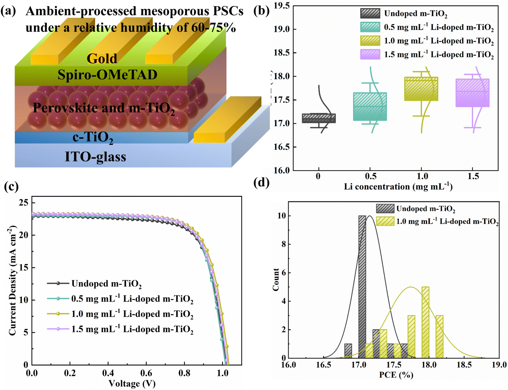 | ||
| Fig. 1 (a) Schematics representation for the ambient-processed mesoscopic PSCs under a RH of 60-75%. (b) PCE distribution and (c) representative J–V curves for PSCs based on the undoped m-TiO2 and Li-doped TiO2. (d) PCE and counts distribution for the PSCs based on the undoped TiO2 and Li-doped m-TiO2 (1.0 mg mL−1). | ||
Having determined the optimal doping concentration of 1.0 mg mL−1 Li-salt to the m-TiO2, we then utilised an ultrafast laser processing method to evaporate the organic binders and introduce the Li doping into m-TiO2. As demonstrated in Fig. 2a, the laser treatment consists of two steps. The first step is to irradiate the m-TiO2 paste and compact TiO2 precursor film coated on the ITO substrate or FTO substrate for 21 s to evaporate binders, induce necking among the TiO2 nanoparticles, and crystallise compact TiO2 films. The second step is to irradiate the m-TiO2 infiltrated with the Li-salt for 21 s to induce the Li doping in m-TiO2. The laser processing setup was modified based on our previous work.25,26,37 The laser setup and detailed parameters are described in the experimental section and Table S2 (ESI†). As shown in Fig. 2b, an FTIR thermal camera was employed to capture temperature changes of m-TiO2 on the ITO substrate treated by different laser programs. Highest annealing temperatures of around 700–750, 800–850, and 900–950 °C were obtained based on three sets of laser parameters. The corresponding thermal images are shown in Fig. S3 (ESI†).
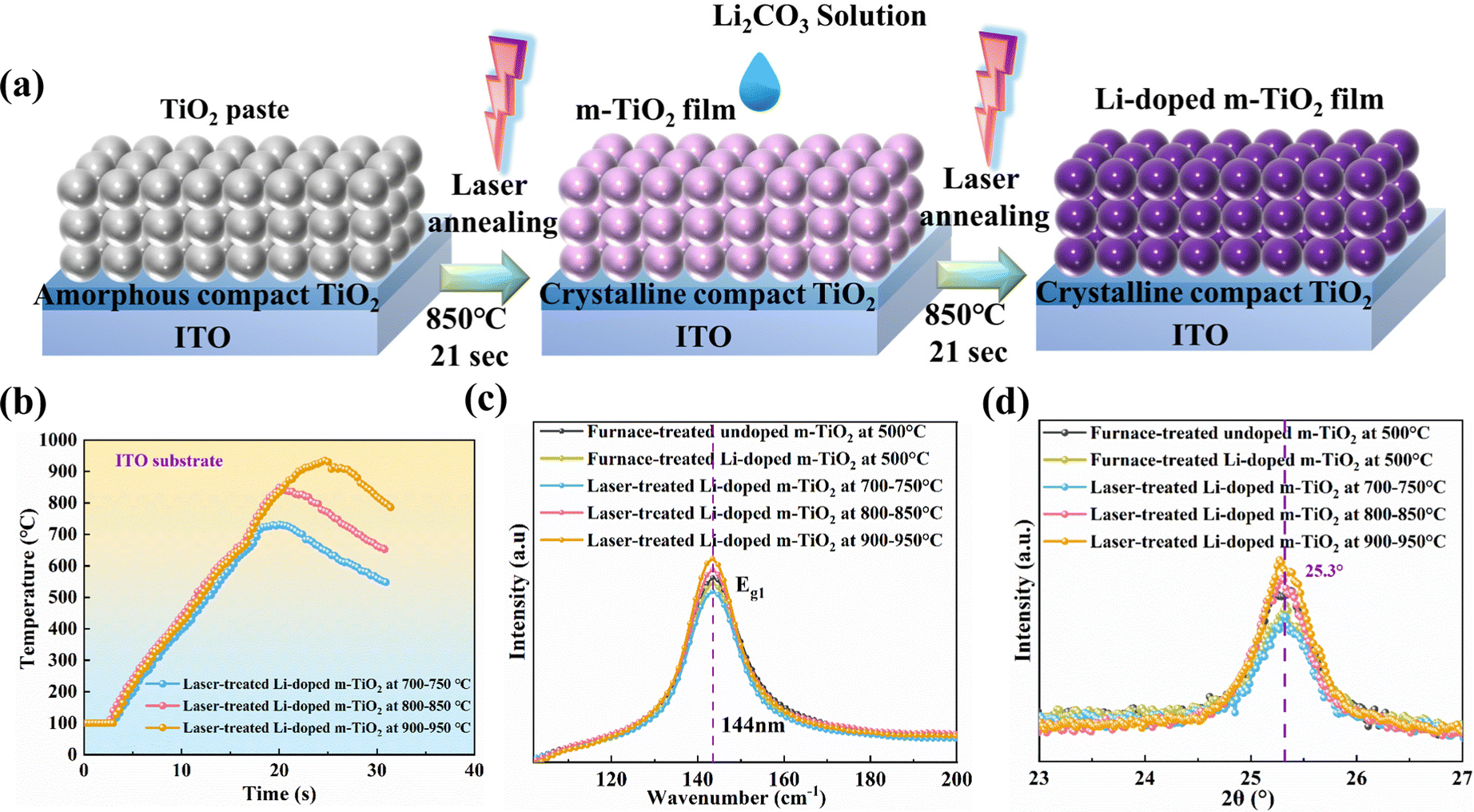 | ||
| Fig. 2 (a) Schematic representation for the Li-doped m-TiO2 prepared by the laser treatment. (b) Temperature profiles for the Li-doped m-TiO2 films coated on ITO substrate measurement during laser treatments. (c) Raman spectra and (d) XRD patterns for the furnace-treated undoped m-TiO2, Li-doped m-TiO2 and laser-treated Li-doped m-TiO2 films. | ||
Raman spectroscopy was conducted to study the crystallinity of the Li-doped m-TiO2 fabricated by conventional method and laser method, as displayed in Fig. S4a (ESI†). All the m-TiO2 films showed peaks at 144, 399, 519 and 639 cm−1, which indicate that TiO2 films exhibit an anatase phase. The Raman peak at 144 cm−1 (Eg1) associated with anatase TiO2 are further zoomed in, as shown in Fig. 2c. The peak intensity for Eg1 decreases after introducing the Li doping into m-TiO2 compared to the undoped m-TiO2. This is due to the presence of Li+ at the interstitial position of the TiO2 lattice that reduces the Ti4+ to Ti3+, resulting in a change of the Raman peak intensity.38 We also noticed that the peak intensity at 144 cm−1 (Eg1) increases with increasing laser annealing temperature, indicating that the crystallinity of the TiO2 film is improved and TiO2 nanoparticles are better necked.39 In addition, the phase transition temperature for TiO2 from anatase to the rutile phase usually happens between 600 °C to 700 °C.40 Nevertheless, no rutile phase has been detected for all laser-treated samples. We believe the short laser processing time (<25 s) contributes to the anatase phase for all these m-TiO2, even with the highest annealing temperatures up to 700–950 °C.
XRD analysis is performed to further investigate the impact of laser treatment on the crystallinity of Li-doped m-TiO2. Fig. S4b (ESI†) shows the XRD patterns of undoped m-TiO2 films and Li-doped m-TiO2 prepared by furnace process and laser process. The XRD confirmed that all these undoped and Li-doped m-TiO2 exhibit the anatase phase, as shown in Fig. 2d. The anatase phase (101) shows a slightly decreased peak intensity after introducing the Li doping compared to the undoped m-TiO2. This might be attributed to the larger ion radius of Li+ (76.0 pm) substituting for the Ti4+ (60.5 pm), causing the distortion of the crystal lattice. Notably, no rutile phase peak is observed in all these m-TiO2 films, which is consistent with the Raman study. In addition, the intensity of (101) peaks increase with increasing laser annealing temperature. The full width at half-maximum (FWHM) for furnace-treated undoped, Li-doped m-TiO2 and laser-treated Li-doped m-TiO2 with the highest annealing temperature of 700–750 °C, 800–850 °C and 900–950 °C are calculated to be 0.638°, 0.653°, 0.726°, 0.628° and 0.617°, respectively. The crystal sizes of m-TiO2 are calculated using the Scherrer equation, summarised in Table S3 (ESI†). We noticed that the crystal size enlarges with the laser processing temperature. The Li-doped m-TiO2 samples treated by laser with the highest annealing temperature of 800–850 °C and 900–950 °C showed larger crystal sizes and smaller FWHM than the furnace-treated sample. We believe that the high annealing temperature achieved by the laser process enhances the necking among TiO2 nanoparticles and improves the film's crystallinity,41 which is consistent with the Raman results. This finding also agrees with the previous study on using flame annealing (around 1000 °C) to treat the m-TiO2 to improve the interconnection between the TiO2 nanoparticles.24
UV-Vis-NIR spectroscopy was performed to investigate the optical properties of the Li-doped m-TiO2 films. As shown in Fig. 3a, we noticed that the laser-treated Li-doped m-TiO2 exhibits higher optical transmission than the furnace-treated samples at wavelengths from 350 to 450 nm, which could improve the perovskite layer's light absorption, resulting in better photovoltaic performance. The optical band gaps (Ebg) of the samples could be obtained from the absorption spectra. The band gap of furnace-treated undoped m-TiO2, Li-doped m-TiO2 and laser-treated Li-doped m-TiO2 films (800–850 °C) are 3.37 eV, 3.38 eV, and 3.40 eV, respectively, as shown in Fig. S5a–c (ESI†).
To study the energy band structure of m-TiO2 films processed by furnace and laser method, UPS was carried out. The magnified valence band edge (Eon-set) acquired from UPS measurement is shown on the left side of Fig. 3b. The secondary electron cutoff edge (Ecut-off) is shown on the right side. The Fermi level (EF) is obtained through an equation: EF = Ecut-off + 18.99 eV – 40.8 eV, where 18.99 eV refers to the bias voltage energy and 40.8 eV refers to the photo energy of He II. The valence band maximum (EVBM) is derived through an equation: EVBM = EF − Eon-set. Combined with the band gap from UV-visible measurement, the conduction band minimum (ECBM) could be calculated based on ECBM = EVBM + Eg.42 The EVBM of furnace-treated undoped m-TiO2, Li-doped m-TiO2 and laser-treated Li-doped m-TiO2 films (800–850 °C) were calculated to be −7.41, −7.47 and −7.48 eV, respectively. Also, the ECBM were calculated to be −4.04 eV, −4.09 eV and −4.08 eV, respectively. The energy level diagram and carrier extraction mechanism of ETL and the perovskite film are displayed in Fig. 3c, and the values are concluded in Table S4 (ESI†). Introducing Li doping into m-TiO2 improves the conduction band alignment between the m-TiO2 and perovskite film. A better band alignment could reduce charge accumulation and recombination, improving charge transport between m-TiO2 and perovskite. A relatively lower EVBM for the Li-doped m-TiO2 than undoped m-TiO2 could be more efficient in blocking holes and suppressing charge recombination.
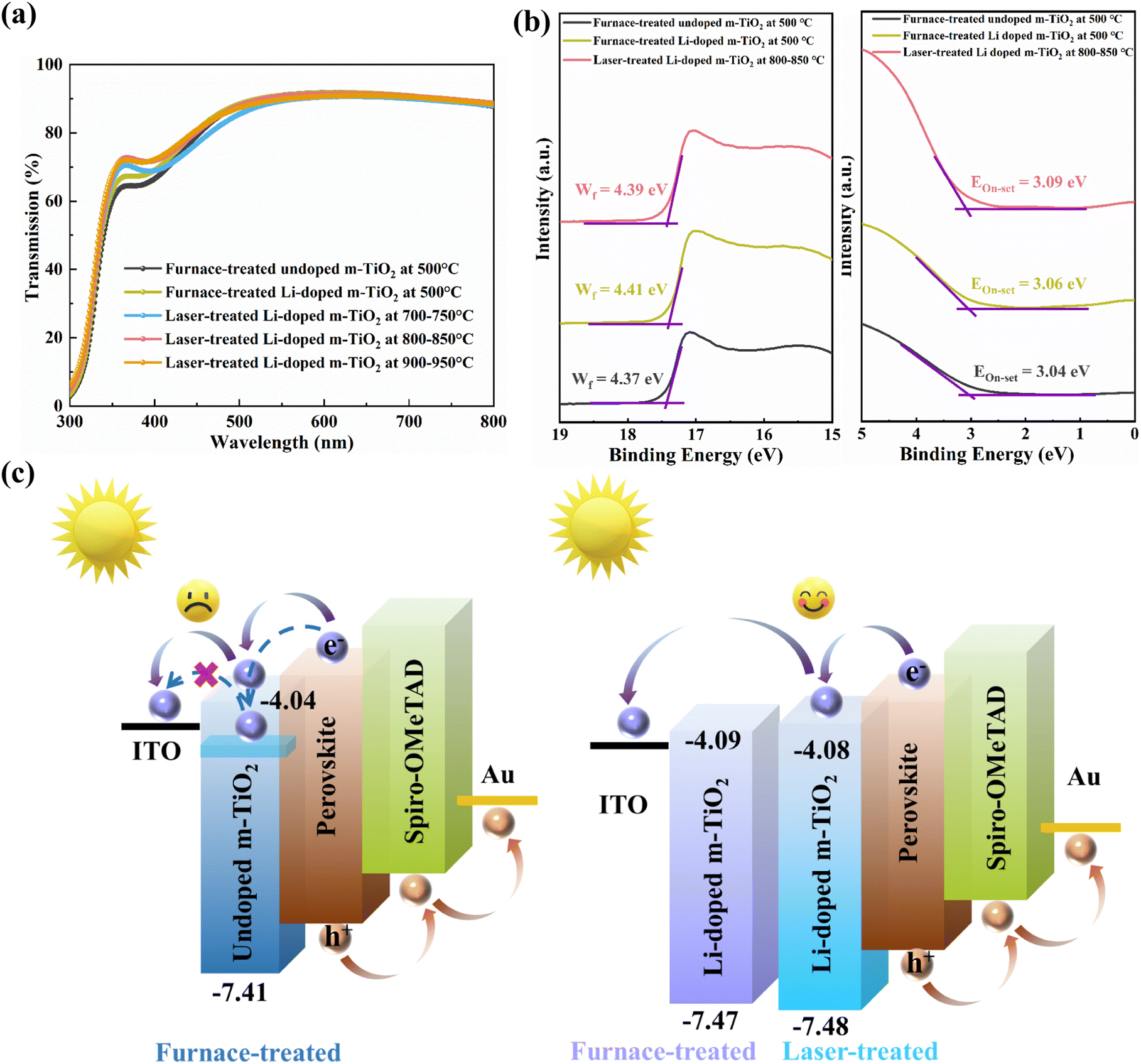 | ||
| Fig. 3 (a) UV-Vis-NIR transmission spectra for the furnace-treated undoped m-TiO2, Li-doped m-TiO2 (1.0 mg mL−1) and laser-treated Li-doped m-TiO2 films with various laser parameters (b) UPS spectra of the furnace-treated undoped m-TiO2, Li doped m-TiO2 (1.0 mg mL−1) and laser-treated Li-doped m-TiO2 films (800–850 °C) showing Ecut-off panel and Eon-set panel, respectively. (c) Energy band diagram and carrier extraction mechanism for the PSCs with furnace-treated undoped m-TiO2, Li-doped m-TiO2 (1.0 mg mL−1) and laser-treated Li-doped m-TiO2 films (800–850 °C). | ||
XPS was conducted to study the elemental composition and surface chemistry changes for undoped and Li-doped m-TiO2 films processed by different treatments. Fig. 4a shows XPS survey spectra and Fig. S6 (ESI†) shows XPS spectra for the Ti 2p3/2 (458.8 eV) and 2p1/2 (464.5eV), corresponding to Ti4+. There is no noticeable change for the Ti 2p3/2 and 2p1/2 peaks before and after introducing Li doping. However, the O 1s located at 530.0 eV for the furnace- and laser-treated Li-doped m-TiO2 shows a noticeable shoulder located at the higher binding energy next to the main peak due to oxygen interaction with the Li, compared to the furnace-treated undoped m-TiO2 as shown in Fig. 4b, in good agreement with the previous studies.5,35,43 The area ratio between the shoulder and main peak for the furnace-treated undoped m-TiO2, furnace- and laser-treated Li-doped m-TiO2 films is calculated to be 0.26, 0.34 and 0.29, respectively, as shown in Table S5 (ESI†). Due to a relatively low Li concentration, the Li 1s peak is not distinguishable, as shown in Fig. 4c. However, the Ti 3s peaks at 63.0 eV are observed in these m-TiO2 films. Notably, the Ti 3s peak intensity for furnace-treated and laser-treated Li-doped m-TiO2 is stronger than that of the furnace-treated undoped m-TiO2, indicating a possible partial Ti4+ reduction to Ti3+ in the m-TiO2 due to presence of Li dopants.44
 | ||
| Fig. 4 (a) XPS survey, (b) O 1s and (c) Ti 3s, Li 1s peaks for the furnace-treated undoped m-TiO2, Li-doped m-TiO2 and laser-treated Li-doped m-TiO2 films. (d) XRD pattern for perovskite films deposited on the furnace-treated undoped m-TiO2, Li-doped m-TiO2 and laser-treated Li-doped m-TiO2 films. | ||
To investigate the crystallinity of the perovskite layer on m-TiO2 films by different treatments, XRD measurement was carried out. Fig. 4d shows the representative XRD patterns corresponding to Cs0.1FA0.9PbI3, in agreement with the previous studies.45 All these perovskite films on furnace- and laser-treated m-TiO2 and Li-doped m-TiO2 exhibit the α-phase Cs0.1FA0.9PbI3. We found no obvious change between the perovskite films deposited on furnace-treated undoped m-TiO2 and furnace-treated Li-doped m-TiO2. Nevertheless, the perovskite deposited on laser-treated Li-doped m-TiO2 with 800–850 °C and 900–950 °C shows a stronger peak intensity corresponding to the α-phase, suggesting enhanced crystallinity and quality of the perovskite layers.
To explore the impact of laser treatment and Li doping on the morphology of m-TiO2 films, SEM was carried out on the top surfaces of different m-TiO2 films. Fig. S7a–e (ESI†) shows the top-view SEM of m-TiO2 films by different treatments. We observe that the TiO2 nanoparticles are necked well, as presented in the purple circles. We then carried out SEM to study the surface morphology and grain size of perovskite film deposited on these m-TiO2 films. All the perovskite films present similar morphology and grain size, as shown in Fig. S8 (ESI†). Besides, the cross-section SEM of devices based on these m-TiO2 films with the configuration of ITO/ETL/perovskite/HTL/Au was also revealed, as shown in Fig. S9 (ESI†).
To evaluate the surface roughness of the ETLs, AFM was carried out on the undoped and Li-doped m-TiO2 films fabricated by different treatments. Fig. S10 (ESI†) presents the root-mean-square roughness (RMS) of these m-TiO2 films, the furnace-treated undoped m-TiO2 shows an RMS of 22.44 nm, while the furnace- and laser-treated Li-doped m-TiO2 films show smoother surfaces with a lower RMS of 18.85 and 16.42 nm, respectively. The smoother surface could improve perovskite deposition, especially for solution deposition methods.46 This could help reduce the contact resistance and recombination rate between the m-TiO2/perovskite interface.47
To explore the change of surface wettability, water contact angle measurement was carried out on the undoped and Li-doped m-TiO2 films fabricated by different treatments. The laser-treated Li-doped m-TiO2 showed a similar water contact angle of 15.1° compared to 14.4° and 14.7° for the furnace-treated undoped and Li-doped m-TiO2, as shown in Fig. S11 (ESI†).
To study the bulk trap-state density of these m-TiO2 films fabricated by different treatments, the dark I–V curves were recorded using SCLC with a device configuration of ITO/c-TiO2/m-TiO2/Au. The I–V curves could be categorised into three regions by equation (J ∝ Vn): the ohmic region (J ∝ V), the trap-free Child's region (J ∝ V2), and the trap-filling limited region (TFL) (J ∝ Vn≥3).48 The I–V curves at a low bias voltage reveal an ohmic contact region with a linear relationship. When the bias voltage increases, the current exhibits a sudden nonlinear increase with a steeper slope, demonstrating the trap-filling limited region. Trap-filled limit voltage (VTFL) represents the point at which the transition occurs from the Ohmic regime to the trap-filled limit (TFL) regime. The trap density, Nt, is obtained by calculating the trap-filled limited voltage through the given equation:49
| Nt = 2VTFLεrε0q−1L−2 | (1) |
The variables used in this study are as follows: VTFL represents the onset voltage of the trap-filled limit region, εr denotes the relative dielectric constant of perovskite (55), ε0 represents the vacuum permittivity (8.854 × 10⁻¹² F m−1), q represents the electron charge (1.6 × 10⁻¹⁹ C), and L represents the thickness of the m-TiO2 film (150 nm).50 As shown in Fig. 5a, the device based on the laser-treated Li-doped m-TiO2 shows the smallest VTFL of 0.58, compared to that of the furnace-treated Li-doped and undoped m-TiO2 film with the VTFL 0.65 V and 0.70 V, respectively. The device based on the laser-treated Li-doped m-TiO2 also gives the lowest trap densities of 1.57 × 1017 cm−3, compared to that of the furnace-treated Li-doped and undoped m-TiO2 film with the values of 1.76 × 1017 cm−3 and 1.89 × 1017 cm−3, as summarised in Table S6 (ESI†). These results indicate that the laser treatment could reduce the trap densities at the perovskite/m-TiO2 interface, possibly due to a soother surface and the reduction of the oxygen vacancies during the high-temperature laser treatment in the air that promotes oxygen incorporation into the TiO2 lattice.26,51 In addition, these results also indicate that Li doping could effectively passivate the trap state in the m-TiO2 film. As reported previously, introducing Li dopant into the TiO2 lattice contributes to a partial reduction of Ti4+ into Ti3+, promoting passivation of the electronic defects due to oxygen vacancies.35,36
 | ||
| Fig. 5 (a) Dark I–V curve for the devices with the furnace-treated undoped m-TiO2, Li-doped m-TiO2 and laser-treated Li-doped m-TiO2 films at 800-850 °C with a structure of ITO/ETL/Au. (b) Steady PL spectra for the perovskite films coated on the furnace-treated undoped m-TiO2, Li-doped m-TiO2 and laser-treated Li-doped m-TiO2 films. (c) Time-resolved PL curves of the perovskite films coated on furnace-treated undoped m-TiO2, Li-doped m-TiO2 and laser-treated Li-doped m-TiO2 films (800–850 °C). (d) Transient photo-voltage decay of PSCs based on furnace-treated undoped m-TiO2, Li-doped m-TiO2 and laser-treated Li-doped m-TiO2 films (800–850 °C). (e) Nyquist plot of devices with furnace-treated undoped m-TiO2, Li-doped m-TiO2 and laser-treated Li-doped m-TiO2 films (800–850 °C). The inset displays the equivalent circuit for the Nyquist plot. | ||
The electrical conductivity of these m-TiO2 films fabricated by different treatments could be calculated from I–V curves at the ohmic region. The conductivity could be determined using the equation:52
| I = σ0AD−1V | (2) |
To further evaluate charge carrier dynamics between the perovskite films deposited on these m-TiO2 films fabricated by different treatments, the steady-state PL and TRPL measurements were performed with a sample structure of ITO/c-TiO2/m-TiO2/perovskite. Fig. 5b displays the PL spectra for the perovskite films on the undoped and Li-doped m-TiO2 films fabricated by different treatments. The sample with furnace-treated Li-doped m-TiO2 shows stronger PL quenching than furnace-treated undoped m-TiO2. In addition, the PL quenching increases first as the laser treatment temperature increases from 700–750 °C to 800–850 °C, followed by a subsequent drop at 900–950 °C. The TRPL plot is fitted according to a bi-exponential decay function, as shown in Fig. 5c.
The calculated proportional fraction and the lifetime are summarised in Table S7 (ESI†). The fast decay τ1 is derived from the charge carrier quenching at the interface between m-TiO2 and perovskite. In contrast, the slow decay τ2 is attributed to the radiative recombination of free charge carriers induced by traps in the bulky perovskite.55 The perovskite deposited on furnace-treated undoped m-TiO2 exhibits the longest lifetime τ1 of 51.34 ns and an average lifetime (τavg) of 238.97 ns. In contrast, the perovskite film deposited on the furnace-treated Li-doped m-TiO2 and laser-treated Li-doped m-TiO2 (800–850 °C) shows shorter τ1 of 50.42 and 31.79 ns, respectively. Besides, they also show the shorter τavg of 168.54 and 162.59 ns. The shorter τ1 and τavg indicate improved electron transport and minimized charge recombination at the interface between the m-TiO2 and perovskite due to Li doping and the laser treatment. The TRPL study is consistent with the SCLC measurement, indicating the benefits of laser treatment and Li doping in improving electron transport and passivating the defects of the Li-doped m-TiO2.
Notably, when the laser treatment temperature reaches 900–950 °C, perovskite film with Li-doped m-TiO2 shows a weaker PL quenching effect than 800–850 °C. To understand the reason behind this, the electrical resistance between two ITO electrodes was tested before and after various treatments, as shown in Fig. S13 and Table S8 (ESI†). The rise of ITO resistance could be due to the conversion of large ITO crystals into equiaxed nanograins under a high-temperature treatment.56 The higher resistance of ITO with laser treatment (900–950 °C) could affect the electron transport, resulting in a weaker PL quenching.
To further investigate the impact of m-TiO2 films fabricated by different treatments on the recombination dynamics and charge transportation of devices, TPV and TPC measurements were conducted by recording the transient electrical response of PSCs with different m-TiO2 films. The TPV is used to measure charge recombination under the open-circuit condition. As shown in Fig. 5d, the TPV curve for the device based on the laser-treated Li-doped m-TiO2 (800–850 °C) presents a slower decay than that of furnace-treated Li-doped and undoped m-TiO2, indicating the suppressed charge recombination.57 Fig. S14 (ESI†) shows the TPC decay for these devices. We noticed that the device based on laser-treated Li-doped m-TiO2 (800–850 °C) exhibits a faster decay rate than that of the furnace-treated Li-doped and undoped m-TiO2, indicating an improved charge transport at the perovskite/m-TiO2 interface.32
The EIS was carried out to further understand the impact of these m-TiO2 films fabricated by different treatments on the electrical dynamics of PSCs. The corresponding Nyquist plots of devices with furnace-treated m-TiO2, furnace- and laser-treated Li-doped m-TiO2 (800–850 °C) were recorded. The EIS fitting plots of PSCs with the equivalent circuit are presented in Fig. 5e, and the calculated value is summarised in Table S9 (ESI†). The PSCs with the furnace-treated Li-doped m-TiO2 showed a smaller series resistance (Rs) of 44.8 Ω and larger recombination resistance (Rrec) of 1542.0 Ω than that of the undoped m-TiO2 with an Rs of 47.6 Ω and Rrec of 1383.0 Ω. The devices based on the Li-doped m-TiO2 exhibit the smallest Rs of 40.4 Ω and largest series resistance Rrec of 3477.0 Ω, indicating that the laser treatment improves charge transport. At the same time, the increased Rrec suggests that the charge recombination is significantly inhibited at the interface and within the bulk material. These results could be attributed to the change of CBM for the m-TiO2 by introducing the Li doping and enhanced interconnection of the TiO2 nanoparticles and interfacial contact between the m-TiO2 and perovskite by the laser treatment. This will help to improve electron transport and suppress charge recombination at both the interface and bulk, consistent with the findings of the PL and TRPL.
To examine the effects of m-TiO2 films fabricated by different treatments on the photovoltaic performance, devices with an n–i–p configuration of ITO-glass/c-TiO2/m-TiO2/perovskite/Spiro-OMeTAD/Au were assembled under a high RH of 60–75%. Fig. 6a illustrates the distribution of PCEs, while Fig. 6b displays the representative J–V curves. Fig. S15 (ESI†) displays the trends of Jsc, Voc, and FF, while Table S10 (ESI†) provides an overview of the photovoltaic performance parameters. PSCs utilising furnace-treated Li-doped m-TiO2 demonstrate an average power conversion efficiency (PCE) of 17.74% and a highest recorded PCE of 18.10%. These cells exhibit a short-circuit current density (Jsc) of 23.34 mA cm−2, an open-circuit voltage (Voc) of 1.027 V, and a fill factor (FF) of 74.03%. On the other hand, the PCE of the PSCs exhibits an upward trend as the laser annealing temperature is raised from 700–750 °C to 800–850 °C, followed by a decline at 900–950 °C. The PSCs using the laser-treated Li-doped m-TiO2 at 800–850 °C exhibit optimised photovoltaics performance with an average PCE of 18.48%, and a highest recorded PCE of 19.15%, Jsc of 23.42 mA cm−2, Voc of 1.038 V, and a FF of 76.08%. The PCE distribution for the PSCs fabricated using laser-treated Li-doped m-TiO2 (800–850 °C) and furnace-treated Li-doped m-TiO2 is presented in Fig. 6c. The improvement of the PCEs by laser treatment could benefit from the boosted electron transport and suppressed charge recombination interconnection of the TiO2 nanoparticles and interfacial contact at m-TiO2/perovskite interface by the laser treatment, which are consistent with the results obtained from Raman, XRD, SCLC, PL, TRPL, and EIS results. Fig. S16 (ESI†) summarises the PCEs for the recent studies on ambient-processed PSCs compared to this work, and Table S11 (ESI†) presents the comparison of laser processing and conditional processing. The external quantum efficiency (EQE) test to confirm the Jsc of PSCs based on laser-treated Li-doped m-TiO2 at 800–850 °C, as shown in Fig. 6d. The integrated current density of the devices was calculated to be 21.46 mA cm−2, slightly lower than the measured Jsc.
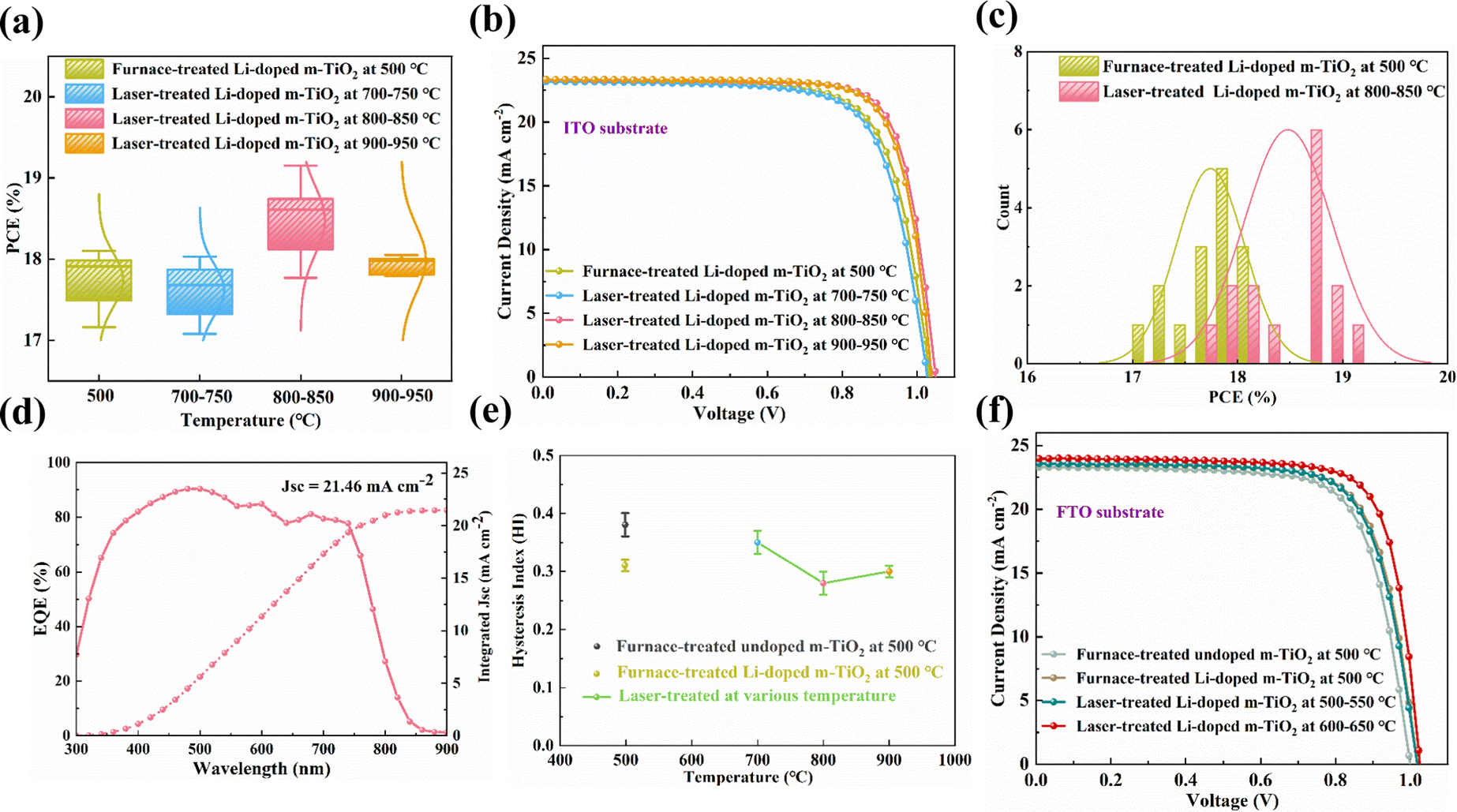 | ||
| Fig. 6 (a) The PCE distribution and (b) representative J–V curves for PSCs with furnace- and laser-treated Li-doped m-TiO2/ITO-glass. (c) PCE and counts distribution for PSCs with furnace- and laser-treated Li-doped m-TiO2 (800–850 °C). (d) EQE and integrated JSC of devices with laser-treated Li-doped m-TiO2 (800–850 °C). (e) Hysteresis index for the PSCs with furnace-treated undoped m-TiO2, Li-doped m-TiO2, and laser-treated Li-doped m-TiO2. (f) Representative J–V curves for PSCs with furnace- and laser-treated Li-doped m-TiO2/FTO-glass. | ||
To understand the impact of mesoscopic structure on the hysteresis behaviour of the device in comparison to the planar device, J–V curves for PSCs based on mesoscopic and planar structures were measured in reverse and forward scans.
The hysteresis index (HI) was calculated as follows:50
 | (3) |
As shown in Fig. S17 (ESI†), we observed a severe hysteresis behaviour for the PSCs based on c-TiO2. (forward PCE of 7.81% and reverse PCE of 17.08% with a hysteresis index of 0.54). On the other hand, with the addition of m-TiO2 and Li-doped m-TiO2, the hysteresis index was remarkably reduced to 0.38, with the lowest hysteresis index achieved by the laser-processed Li-doped m-TiO2 (0.28), as shown in Fig. 6e. The corresponding HI are summarised in Table S12 (ESI†). Therefore, using a mesoscopic structure significantly suppressed the hysteresis behaviour of our ambient-processed PSCs. We believe this finding is possibly due to a combination of enhanced charge separation and improved perovskite film crystallisation in ambient air with the presence of m-TiO2.58,59 In addition, the use of m-TiO2 can act as a protective layer to reduce the moisture ingress into the perovskite crystals infiltrated within the mesoscopic structure, resulting in enhanced device stability.60,61 These results further confirmed that the laser treatment could improve electron transport and suppress the charge accumulation and charge recombination occurring at the interface between perovskite and TiO2.
To exclude the impact of different treatments on the electrical resistance of the ITO electrodes that could affect the photovoltaic efficiency of PSCs, we further fabricated PSCs on laser-treated m-TiO2/FTO substrates. Fig. S18 (ESI†) shows the temperature changes for the Li-doped m-TiO2 films coated on FTO-glass by laser processing with the highest annealing temperature of 500–550 and 600–650 °C. The thermal profiles during the laser processing are displayed in Fig. S19 (ESI†), while the parameters are included in Table S2 (ESI†). Interestingly, under identical laser processing conditions, the laser treatment of m-TiO2 films on ITO-glass results in higher annealing temperatures of 700–750 and 800–850 °C, respectively. This can be attributed to the superior photo-thermal conversion efficiency of ITO in comparison to FTO.25,62
The representative J–V curves for the PSCs with furnace-treated undoped m-TiO2, furnace- and laser-treated Li-doped m-TiO2 are shown in Fig. 6f. The device using laser-treated Li-doped m-TiO2 (600–650 °C) offers the highest PCE of 18.95% compared to the furnace-treated undoped m-TiO2 and Li-doped m-TiO2 with 17.01% and 18.10%, respectively. These results further confirmed that the laser treatment could enhance the photovoltaic performance of the PSCs, regardless of whether they are on ITO or FTO substrates.
4. Conclusion
In this study, we presented an ultrafast laser process for fabricating Li-doped m-TiO2 for mesoscopic PSCs that only needs 42 s laser processing with the highest annealing temperature of 800–850 °C. Not only does the laser process effectively shorten the fabrication time, but it also improves the electron transport ability and suppresses charge recombination and hysteresis behaviour due to the enhanced interconnection between the TiO2 nanoparticles, reduced oxygen vacancies and improved interfacial contact at the perovskite/m-TiO2. Consequently, ambient-processed PSCs with laser-treated Li-doped m-TiO2 showed a champion PCE of 19.15% in contrast with the furnace-treated one of 18.10%. The laser process provides a promising approach to fabricating metal-doped m-TiO2 films for PSCs and related applications.Author contributions
Hongbo Mo: conceptualization, investigation, methodology, data curation, formal analysis, writing – original draft. Qian Chen: conceptualization, methodology, investigation, formal analysis, validation, funding acquisition, supervision, writing – review & editing. Dong Wang: investigation, data curation, writing – review & editing. wei guo: investigation, methodology. Dongxu Cheng: investigation, data curation. Yang Sha: investigation, data curation. Muhamad Z. Mokhtar: investigation, data curation. Zhenyu Jia: investigation, data curation. Janet Jacobs: data curation, formal analysis. Andrew G. Thomas: resources, formal analysis, writing – review & editing. Lin Li: resources, supervision. Zhu Liu: resources, supervision, funding acquisition. Richard J. Curry: formal analysis, resources, funding acquisition, writing – review & editing.Conflicts of interest
The authors declare no competing financial interest.Acknowledgements
This study received financial support from the Engineering and Physical Sciences Research Council (EPSRC) through grant no. EP/V008188/1. Hongbo Mo expresses gratitude to The China Scholarship Council-The University of Manchester joint scholarship for his doctoral studies. The authors express gratitude for the support received from the Department of Materials X-ray Diffraction Suite at the University of Manchester, as well as the technical assistance provided by Dr Gary Harrison. The authors express their gratitude to Dr Marek Nikiel from the Photon Science Institute, Department of Materials at the University of Manchester, for his assistance with AFM measurements. The authors express their gratitude to Dr Khaled Parvez from the Department of Chemistry at The University of Manchester for his assistance in conducting water contact angle measurements. The authors express their gratitude for the utilisation of the Department of Materials XPS at the University of Manchester and the technical assistance provided by Dr Ben Spencer.References
- W. Zhang, Y. Tian, H. He, L. Xu, W. Li and D. Zhao, Nat. Sci. Rev., 2020, 7, 1702–1725 CrossRef CAS.
- A. Hadi, Q. Chen, M. Curioni, R. Xiao, T. Huang and Z. Liu, ACS Sustainable Chem. Eng., 2018, 6, 12299–12308 CrossRef CAS.
- M. J. Paik, Y. Lee, H. S. Yun, S. U. Lee, S. T. Hong and S. Il Seok, Adv. Energy Mater., 2020, 10, 1–7 CrossRef.
- C. Zhen, T. Wu, R. Chen, L. Wang, G. Liu and H. M. Cheng, ACS Sustainable Chem. Eng., 2019, 7, 4586–4618 CrossRef CAS.
- F. Giordano, A. Abate, J. P. Correa Baena, M. Saliba, T. Matsui, S. H. Im, S. M. Zakeeruddin, M. K. Nazeeruddin, A. Hagfeldt and M. Graetzel, Nat. Commun., 2016, 7, 1–6 Search PubMed.
- F. Wu, S. Lu, C. Hu, H. Lu, C. Chen, J. Tang, S. Yang and L. Zhu, Adv. Sustainable Syst., 2022, 2200212, 1–8 Search PubMed.
- M. Kim, I. Woo Choi, S. J. Choi, J. W. Song, S. I. Mo, J. H. An, Y. Jo, S. J. Ahn, S. K. Ahn, G. H. Kim and D. S. Kim, Joule, 2021, 5, 659–672 CrossRef CAS.
- M. Li, Y. Zhao, L. Zhu, J. Song and Y. Qiang, J. Mater. Sci.: Mater. Electron., 2019, 30, 9038–9044 CrossRef CAS.
- J. Yue, C. Suchomski, P. Voepel, R. Ellinghaus, M. Rohnke, T. Leichtweiss, M. T. Elm and B. M. Smarsly, J. Mater. Chem. A, 2017, 5, 1978–1988 RSC.
- S. H. Chen, C. M. Ho, Y. H. Chang, K. M. Lee and M. C. Wu, Chem. Eng. J., 2022, 445, 136761 CrossRef CAS.
- M. C. Wu, S. H. Chan, K. M. Lee, S. H. Chen, M. H. Jao, Y. F. Chen and W. F. Su, J. Mater. Chem. A, 2018, 6, 16920–16931 RSC.
- S. K. Pathak, A. Abate, P. Ruckdeschel, B. Roose, K. C. Gödel, Y. Vaynzof, A. Santhala, S. I. Watanabe, D. J. Hollman, N. Noel, A. Sepe, U. Wiesner, R. Friend, H. J. Snaith and U. Steiner, Adv. Funct. Mater., 2014, 24, 6046–6055 CrossRef CAS.
- Z. Xu, J. Wu, T. Wu, Q. Bao, X. He, Z. Lan, J. Lin, M. Huang, Y. Huang and L. Fan, Energy Technol., 2017, 5, 1820–1826 CrossRef CAS.
- B. Roose, K. C. Gödel, S. Pathak, A. Sadhanala, J. P. C. Baena, B. D. Wilts, H. J. Snaith, U. Wiesner, M. Grätzel, U. Steiner and A. Abate, Adv. Energy Mater., 2016, 6, 1–7 Search PubMed.
- J. K. Kim, S. U. Chai, Y. Ji, B. Levy-Wendt, S. H. Kim, Y. Yi, T. F. Heinz, J. K. Nørskov, J. H. Park and X. Zheng, Adv. Energy Mater., 2018, 8, 1–7 Search PubMed.
- M. Saliba, T. Matsui, K. Domanski, J.-Y. Seo, A. Ummadisingu, S. M. Zakeeruddin, J.-P. Correa-Baena, W. R. Tress, A. Abate, A. Hagfeldt and M. Grätzel, Science, 2016, 354, 206–209 CrossRef CAS PubMed.
- K. T. Cho, S. Paek, G. Grancini, C. Roldán-Carmona, P. Gao, Y. Lee and M. K. Nazeeruddin, Energy Environ. Sci., 2017, 10, 621–627 RSC.
- I. Turkevych, S. Kazaoui, N. A. Belich, A. Y. Grishko, S. A. Fateev, A. A. Petrov, T. Urano, S. Aramaki, S. Kosar, M. Kondo, E. A. Goodilin, M. Graetzel and A. B. Tarasov, Nat. Nanotechnol., 2019, 14, 57–63 CrossRef CAS PubMed.
- T. J. Macdonald, M. Batmunkh, C.-T. Lin, J. Kim, D. D. Tune, F. Ambroz, X. Li, S. Xu, C. Sol, I. Papakonstantinou, M. A. McLachlan, I. P. Parkin, J. G. Shapter and J. R. Durrant, Small Methods, 2019, 3, 1900164 CrossRef CAS.
- A. Peter Amalathas, L. Landová, K. Ridzoňová, L. Horák, P. Bauerová and J. Holovský, ACS Appl. Energy Mater., 2021, 4, 11488–11495 CrossRef CAS.
- S. Sidhik, A. Cerdan Pasarán, D. Esparza, T. López Luke, R. Carriles and E. De La Rosa, ACS Appl. Mater. Interfaces, 2018, 10, 3571–3580 CrossRef CAS.
- D. A. R. Barkhouse, O. Gunawan, T. Gokmen, T. K. Todorov and D. B. Mitzi, Prog. Photovoltaics Res. Appl., 2015, 20, 6–11 CrossRef.
- J. Shen, D. J. Green, R. E. Tressler and D. L. Shelleman, J. Non. Cryst. Solids, 2003, 324, 277–288 CrossRef CAS.
- J. K. Kim, S. U. Chai, Y. Cho, L. Cai, S. J. Kim, S. Park, J. H. Park and X. Zheng, Small, 2017, 13, 1–7 CAS.
- Q. Chen, W. Guo, J. C. R. Ke, M. Z. Mokhtar, D. Wang, J. Jacobs, A. G. Thomas, R. J. Curry and Z. Liu, Sol. RRL, 2021, 5, 1–10 Search PubMed.
- H. Mo, D. Wang, Q. Chen, W. Guo, S. Maniyarasu, A. G. Thomas, R. J. Curry, L. Li and Z. Liu, ACS Appl. Mater. Interfaces, 2022, 14, 15141–15153 CrossRef CAS PubMed.
- J. F. Guayaquil-Sosa, B. Serrano-Rosales, P. J. Valadés-Pelayo and H. de Lasa, Appl. Catal., B, 2017, 211, 337–348 CrossRef CAS.
- S. Bibi, S. S. Shah, F. Muhammad, M. Siddiq, L. Kiran, S. A. Aldossari, M. Sheikh Saleh Mushab and S. Sarwar, Chemosphere, 2023, 339, 139583 CrossRef CAS PubMed.
- Z. Ali, S. N. Cha, J. I. Sohn, I. Shakir, C. Yan, J. M. Kim and D. J. Kang, J. Mater. Chem., 2012, 22, 17625–17629 RSC.
- F. Amri, N. L. W. Septiani, M. Rezki, M. Iqbal, Y. Yamauchi, D. Golberg, Y. V. Kaneti and B. Yuliarto, J. Mater. Chem. B, 2021, 9, 1189–1207 RSC.
- B. Niu, X. Wang, K. Wu, X. He and R. Zhang, Material, 2018, 11 Search PubMed.
- D. Wang, Q. Chen, H. Mo, J. Jacobs, A. Thomas and Z. Liu, Mater. Adv., 2020, 1, 2057–2067 RSC.
- H. Mo, Q. Chen, D. Wang, D. Cheng, S. Maniyarasu, M. Z. Mokhtar, J. Jacobs, T. L. See, A. G. Thomas, R. J. Curry, L. Li and Z. Liu, Sol. RRL, 2022, 6, 2200798 CrossRef CAS.
- Q. Chen, J. C.-R. Ke, D. Wang, M. Z. Mokhtar, A. G. Thomas and Z. Liu, Appl. Surf. Sci., 2021, 536, 147949 CrossRef CAS.
- D. Liu, S. Li, P. Zhang, Y. Wang, R. Zhang, H. Sarvari, F. Wang, J. Wu, Z. Wang and Z. D. Chen, Nano Energy, 2017, 31, 462–468 CrossRef CAS.
- A. Peter Amalathas, L. Landová, B. Conrad and J. Holovský, J. Phys. Chem. C, 2019, 123, 19376–19384 CrossRef CAS.
- Q. Chen, M. Z. Mokhtar, J. C.-R. Ke, A. G. Thomas, A. Hadi, E. Whittaker, M. Curioni and Z. Liu, Sustain, Energy Fuels, 2018, 2, 1216–1224 CAS.
- A. Vázquez-López, D. Maestre, R. Martínez-Casado, J. Ramírez-Castellanos, I. Píš, S. Nappini and A. Cremades, J. Mater. Sci., 2022, 57, 7191–7207 CrossRef.
- I. I. Kabir, L. R. Sheppard, R. Shamiri, P. Koshy, R. Liu, W. Joe, A. Le, X. Lu, W.-F. Chen and C. C. Sorrell, J. Mater. Sci., 2020, 55, 3774–3794 CrossRef CAS.
- C. Byrne, R. Fagan, S. Hinder, D. E. McCormack and S. C. Pillai, RSC Adv., 2016, 6, 95232–95238 RSC.
- M. C. Mathpal, A. K. Tripathi, M. K. Singh, S. P. Gairola, S. N. Pandey and A. Agarwal, Chem. Phys. Lett., 2013, 555, 182–186 CrossRef CAS.
- M. Park, J. Y. Kim, H. J. Son, C. H. Lee, S. S. Jang and M. J. Ko, Nano Energy, 2016, 26, 208–215 CrossRef CAS.
- S. Södergren, H. Siegbahn, H. Rensmo, H. Lindström, A. Hagfeldt and S. E. Lindquist, J. Phys. Chem. B, 1997, 101, 3087–3090 CrossRef.
- C. L. Olson, J. Nelson and M. Saiful Islam, J. Phys. Chem. B, 2006, 110, 9995–10001 CrossRef CAS.
- N. Li, J. Liu, C. Li, Y. Li, J. Jia, Y. Wu, H. Yu, B. Yuan and B. Cao, ACS Sustainable Chem. Eng., 2020, 8, 7020–7030 CrossRef CAS.
- X. H. Zhang, J. J. Ye, L. Z. Zhu, H. Y. Zheng, X. P. Liu, X. Pan and S. Y. Dai, ACS Appl. Mater. Interfaces, 2016, 8, 35440–35446 CrossRef CAS PubMed.
- J. Y. Kim, S. Rhee, H. Lee, K. An, S. Biswas, Y. Lee, J. W. Shim, C. Lee and H. Kim, Adv. Mater. Interfaces, 2020, 7, 1902003 CrossRef CAS.
- A. Carbone, C. Pennetta and L. Reggiani, Appl. Phys. Lett., 2009, 95, 2007–2010 Search PubMed.
- Q. Dong, Y. Fang, Y. Shao, P. Mulligan, J. Qiu, L. Cao and J. Huang, Science, 2015, 347, 967–970 CrossRef CAS.
- X. Shi, Y. Ding, S. Zhou, B. Zhang, M. Cai, J. Yao, L. Hu, J. Wu, S. Dai and M. K. Nazeeruddin, Adv. Sci., 2019, 6, 1901213 CrossRef CAS PubMed.
- P. Mazzolini, T. Acartürk, D. Chrastina, U. Starke, C. S. Casari, G. Gregori and A. L. Bassi, Adv. Electron. Mater., 2016, 2, 1–9 Search PubMed.
- R. H. Bube, J. Appl. Phys., 1962, 33, 1733–1737 CrossRef CAS.
- R. Teimouri, Z. Heydari, M. P. Ghaziani, M. Madani, H. Abdy, M. Kolahdouz and E. Asl-Soleimani, Superlattices Microstruct., 2020, 145, 106627 CrossRef CAS.
- J. H. Heo, M. S. You, M. H. Chang, W. Yin, T. K. Ahn, S. J. Lee, S. J. Sung, D. H. Kim and S. H. Im, Nano Energy, 2015, 15, 530–539 CrossRef CAS.
- F. Gao, C. Luo, X. Wang and Q. Zhao, Small Methods, 2021, 5, 1–9 Search PubMed.
- W. L. Hsu, Y. H. Pai, F. S. Meng, C. W. Liu and G. R. Lin, Appl. Phys. Lett., 2009, 94, 231906 CrossRef.
- H. Tan, A. Jain, O. Voznyy, X. Lan, F. P. García de Arquer, J. Z. Fan, R. Quintero-Bermudez, M. Yuan, B. Zhang, Y. Zhao, F. Fan, P. Li, L. N. Quan, Y. Zhao, Z.-H. Lu, Z. Yang, S. Hoogland and E. H. Sargent, Science, 2017, 355, 722–726 CrossRef CAS PubMed.
- M. F. Mohamad Noh, N. A. Arzaee, I. N. Nawas Mumthas, N. A. Mohamed, S. N. F. Mohd Nasir, J. Safaei, A. R. bin, M. Yusoff, M. K. Nazeeruddin and M. A. Mat Teridi, J. Mater. Chem. A, 2020, 8, 10481–10518 RSC.
- H. S. Kim and N. G. Park, J. Phys. Chem. Lett., 2014, 5, 2927–2934 CrossRef CAS.
- J. Yin, J. Cao, X. He, S. Yuan, S. Sun, J. Li, N. Zheng and L. Lin, J. Mater. Chem. A, 2015, 3, 16860–16866 RSC.
- J. Yang, K. M. Fransishyn and T. L. Kelly, Chem. Mater., 2016, 28, 7344–7352 CrossRef CAS.
- T. Jeon, H. M. Jin, S. H. Lee, J. M. Lee, H. Il Park, M. K. Kim, K. J. Lee, B. Shin and S. O. Kim, ACS Nano, 2016, 10, 7907–7914 CrossRef CAS PubMed.
Footnotes |
| † Electronic supplementary information (ESI) available. See DOI: https://doi.org/10.1039/d3tc03151a |
| ‡ These authors have contributed equally to this work. |
| This journal is © The Royal Society of Chemistry 2024 |