
 Open Access Article
 This Open Access Article is licensed under a Creative Commons Attribution-Non Commercial 3.0 Unported Licence
Assessing the electronic and optical properties of lanthanum diselenide: a computational study†
Lanjing
Huo‡
a and
Christopher N.
Savory‡
 *abc
*abc
aDepartment of Chemistry, University College London, Christopher Ingold Building, London WC1H 0AJ, UK. E-mail: uccacns@ucl.ac.uk
bThomas Young Centre, University College London, Gower Street, London WC1E 6BT, UK
cSchool of Chemistry, University of Birmingham, Edgbaston, Birmingham, B15 2TT, UK
First published on 17th April 2024
Abstract
The lanthanide polychalcogenides are a diverse family of compounds with numerous tuneable properties, but only recently has stoichiometric LaSe2 been proposed as a hole transport material. Clarification over its electronic, optical and transport properties is necessary for its future development as a functional material – in this work, we perform hybrid density functional theory calculations to examine and assess these properties. We find that LaSe2 has strongly anisotropic hole transport properties due to the valence band maximum comprising π antibonding interactions in Se–Se dimers, and a resultant two order of magnitude difference in predicted mobilities between in- and out-of-plane directions. An indirect gap together with forbidden electronic transitions is predicted to lead to a delayed onset of optical absorption, making LaSe2 a strong candidate for an IR-transparent hole conducting material.
1 Introduction
The rare earth polychalcogenides demonstrate a number of interesting electronic and structural properties related to their compositional flexibility and layered structure: multiple non-stoichiometric LnCh2−x phases have been synthesised in the past several decades1–4 and the compound family draws comparisons with the transition metal dichalcogenides with their tunability. While the lanthanum polychalcogenides do not exhibit the magnetic behaviour associated with the valence 4f states later in the rare earth series, since superconductivity was found in the intermediate phases between La2Se3 and La3Se4,5 the lanthanum selenides have been no less popular, and represent a fertile ground for solid-state materials research.Recently, stoichiometric lanthanum diselenide (LaSe2) has been highlighted as a potential stable p-type conductive material with transparency in the near to mid-infrared region, with its high achievable conductivity and small hole effective mass relative to other p-type IR-transparent conducting materials (TCMs), such as the delafossite family, noted as key advantages.6,7 p-type TCMs are crucial to the development of more efficient optoelectronic devices including photovoltaics, display monitors and especially smart windows, dependent on which frequencies of light the material is transparent to. Across various spectral ranges, however, p-type TCM performance typically lags well behind their n-type counterparts, primarily due to the difficulty in engineering band dispersion in the valence bands of semiconductors.8 To achieve high hole mobilities in oxides, hybridization of cation states with oxygen 2p states at the top of the valence band has been seen as key to such engineering,9,10 though recent high-throughput searches have explored chalcogenides and phosphides with varied valence band configurations as alternative p-type TCMs.11,12 With promising initial transport measurements, LaSe2 warrants further investigation to understand the origin of its optical and electronic behaviour, as well as exploring its optical and transport properties for potential integration into future devices.
The structure of LaSe2 has received multiple prior studies, with added complexity due to the stability of the LaSe1.9 selenium-deficient phase in the La–Se phase diagram.13 Both compounds have been seen to relate to the tetragonal (P4/nmm) anti-Fe2As and ZrSSi structure types, with a double layer of La–Se alternating with a single-layered square lattice of Se atoms (Fig. 1(a)). In stoichiometric LaSe2, to balance the charge of La3+, the Se atoms have a formal oxidation state of −1.5 when averaged over the whole formula unit. The differing symmetry environments within the cell, however, suggest mixed valency with an ionic Se2− in the double layer (situated in the P21/c cell at 0.36a, 0.63a) and Se− in the square lattice (0, a), the latter potentially forming a part-filled Se p band and metallic conductivity. A Peierls-type distortion can be considered, however, wherein each pair of neighbouring Se in the square-lattice layer will distort towards each other and form an Se–Se bond along the basal plane, creating the stable polychalcogenide species Se22− (analogous to the peroxide ion for oxygen) and lowering the symmetry; we might expect an associated electronic transition from a 2D metal to an insulating phase, which is then consistent with the observed semiconducting behaviour above. The Se–Se distortions pair, distorting in opposite directions such that the Se22− dimers form an offset ‘herringbone’ type pattern (similar to the arrangement of I2 in the solid state)14 and doubling the unit cell along either the tetragonal a or b directions. The resultant P21/c structure (Fig. 1(b) and (c), the latter specifically showing the Se–Se bonding), with two forms available via twinning, was found by Benazeth et al. in 1980,15 with further confirmation by McMillan and co-workers in 199613 – prior reports of tetragonal LaSe2 may be expected to instead be LaSe1.9.16,17 Synthesis conditions may play a key role, with selenium-deficient phases accessible by low-temperature solution-based synthetic routes,18,19 while the stoichiometric phase has required high-temperature traditional solid-state synthesis or magnetron sputtering.6,20
 | ||
| Fig. 1 Crystal Structures of LaSe2 in the previously reported (a) P4/nmm and (b), (c) P21/c space groups. La atoms are in purple and Se atoms are in green, and Se–Se bonding is included within the P21/c unit cell. La–Se bonding is not included in (c) and the structure is viewed along [100] to illustrate the Se–Se dimerization. | ||
The other closed–shell LnCh2 −x (Ln = La, Lu; Ch = S, Se) compounds have also been suggested to belong to the anti-Fe2As structure type, though with similar ambiguity over the possibility of Ch–Ch bonding. Initial structural studies on LaS2 suggested tetragonal space groups – either P4/nmm21 or P![[4 with combining macron]](https://www.rsc.org/images/entities/char_0034_0304.gif) nb22 – however, similarly to LaSe2, distorted structures have been proposed as well: Pnma in 1978,23 and a P21/a structure similar to that of monoclinic LaSe2 in 1994.4 The Pnma structure also contains a herring-bone arrangement of S–S dimers, though the unit cell is doubled perpendicular to the layers due to a small offsetting of the La atoms, and this assignment has been supported by a more recent study.24 LuSe2, in contrast, has only been recorded experimentally as belonging to the P4/nmm structure type.25 As such, there is clear motivation to explore the structural behaviour of these systems, clarify the identity of the ground-state structures, and establish the electronic characteristics that result.
nb22 – however, similarly to LaSe2, distorted structures have been proposed as well: Pnma in 1978,23 and a P21/a structure similar to that of monoclinic LaSe2 in 1994.4 The Pnma structure also contains a herring-bone arrangement of S–S dimers, though the unit cell is doubled perpendicular to the layers due to a small offsetting of the La atoms, and this assignment has been supported by a more recent study.24 LuSe2, in contrast, has only been recorded experimentally as belonging to the P4/nmm structure type.25 As such, there is clear motivation to explore the structural behaviour of these systems, clarify the identity of the ground-state structures, and establish the electronic characteristics that result.
In this paper, we aim to explore the structural, electronic and optical properties of stoichiometric LaSe2 in greater depth using ab initio computational techniques with an aim to assessing its future capabilities as an IR-transparent hole conducting material. We use hybrid density functional theory (DFT) calculations to ensure the accuracy of our predictions, with further support for our predicted electronic structures using many-body perturbation theory. From there, we calculate the optical absorption as well as the predicted electronic transport properties of LaSe2 critical for its application; herein, we move beyond the constant relaxation time approximation typically used for ab initio calculations of transport properties to explicitly simulating the scattering rates for key scattering mechanisms, and their resultant effect on the materials mobility. Throughout, we aim to understand how the structural features of LaSe2 influence the electronic properties, and make a critical assessment of its future as a functional material.
2 Computational methods
DFT calculations were performed within periodic boundary conditions using the Vienna Ab Initio Simulation Package (VASP).26–29 Within VASP, the projector augmented wave method is used to describe core-valence electron interactions,30 using scalar-relativistic pseudopotentials with the following configurations: La [Kr 4d10] 5s2 5p6 6s2 5d1; Se [Ar3d10] 4s2 4p4. Multiple DFT functionals were trialled to assess the most suitable method to describe the structural, electronic and optical properties of LaSe2: the generalized gradient approximation functionals PBE31 and PBEsol32 were trialled for the purpose of vibrational properties, while the hybrid DFT functionals HSE0633,34 and PBE035 were used for electronic structure and optical properties, to avoid the severe underestimation of semiconductor band gaps in standard DFT. Convergence of the k-point mesh and plane-wave cutoff energy was determined for LaSe2 once the total energy was found to be within 1 meV per atom – corresponding to a plane wave cutoff of 350 eV and k-mesh of 4 × 8 × 4 – these settings were used for the electronic structure calculations. Supporting calculations were performed on LaS2 and LuSe2 – for these, a plane wave cutoff of 400 eV and k-meshes of 5 × 2 × 8 and 9 × 9 × 5 respectively were found to converge the total energy to the same criterion. During the initial geometrical optimization of the structure, the structure was considered to be converged once the forces on each atom were below 0.01 eV Å−1 and the cutoff energy was increased to 560 eV to account for the effects of Pulay stress. For calculations of the phonon spectrum and vibrational properties, the supercell displacement method was used with the code Phonopy,36 and the structure was relaxed to a tighter tolerance: 0.1 meV Å−1 on the forces per atom, and 1 × 10⁻⁸ meV on the total energy, using a similarly raised cutoff energy. Non-analytical corrections were included, with Born effective masses taken from density functional perturbation theory (DFPT) calculations performed under the same convergence criteria. 2 × 4 × 2 and 4 × 4 × 2 supercells (both 192 atoms) were used for the P21/c and P4/nmm structures respectively (2 × 1 × 4 and 4 × 4 × 2 supercells were used for LaS2 and LuSe2 respectively). The PhonopySpectroscopy package was used to aid in the calculation of (spherically-averaged) theoretical Infra-Red (IR) and Raman intensities.37Further convergence was necessary for the optical properties, with the high-frequency dielectric constant found to be converged to within 0.01 at a k-mesh of 6 × 12 × 6 and >200 total electronic bands – this optical data was also used for the calculation of the spectroscopically limited maximum efficiency and the Blank et al. metrics,38,39 which require a calculated absorption spectrum (and refractive index in the case of Blank et al.). These two metrics have been used to assess the suitability of various materials as thin-film absorbers for solar cells – while neither are theoretical efficiencies, they work to improve screening of candidate photovoltaic materials beyond the detailed balance limit by introducing realistic absorption profiles, as well as mechanisms to consider the impact of forbidden or indirect band gaps, and potential non-radiative recombination. A more detailed description of the assumptions these metrics use is included in the ESI.† Plotting of all densities of states and electronic structures made use of the sumo package, as well as extraction of curvature/band effective masses through a parabolic fit to the band edges.40
For further assessment of the band gap of LaSe2, the quasiparticle self-consistent GW (QSGW) method of Kotani et al.41 was used within the Questaal package.42 Questaal is capable of performing QSGW and DFT methods using a full-potential linear muffin-tin orbital (FP-LMTO) basis set. For LaSe2, the code-generated augmentation spheres and interstitial smoothed Hankel function basis sets were used for each structure, with a l-cutoff of 4 used for both La and Se, and muffin tin radii of 3.3 a.u. for La and 2.3 a.u. for Se. A k-mesh of 4 × 8 × 4 was used for all QSGW calculations, a G-cutoff for the interstitial plane waves of 6.4 Ry1/2, and the QSGW method was iterated until the root-mean-square (RMS) change in the self-energy, Σ0, was below 1 × 10⁻⁵. QSGW, while capable of predicting accurate band gaps for various semiconductors, is known to systematically overestimate band gaps due to the random phase approximation (RPA) omitting key screening effects. To further improve the method, ladder diagrams, which include explicit electron–hole screening, were included in the screened Coulomb interaction W – within this QSGŴ method,43 the self-energy was solved self-consistently with the same convergence criterion for Σ0 and using 6 occupied and 6 unoccupied states within the Bethe–Salpeter equation (sufficient to converge the electronic gap to within 0.01 eV). Such QSGŴ calculations have previously been shown to replicate the gaps of semiconductors with exceptional accuracy.44,45 Convergence of the QSGŴ was confirmed as increasing the GW k-mesh to 5 × 9 × 5 or the number of occupied and unoccupied states to 7 lead to no more than a 10 meV change in the band gap.
Transport properties were calculated using a dense electronic structure calculation (10 × 20 × 10 k-mesh, then further interpolated – see ESI,† Fig. S8) through the package AMSET.46 AMSET goes beyond the constant relaxation time approximation by simulating, using ab initio calculated materials properties such as the static dielectric constant, the dominant electronic scattering processes: acoustic deformation potential, polar optical phonon and ionized impurity scattering. Description of the specific scattering models are included on the AMSET website (https://hackingmaterials.lbl.gov/amset/) and in the ESI.† In this way, it is possible to obtain a more sophisticated analysis of the contributions to the overall carrier mobility, and more accurate predictions of conductivity limits for real devices.
3 Results and discussion
As discussed above, two structure types have been proposed for LaSe2, so we initially investigate both (P21/c15 and P4/nmm16) phases using both hybrid and standard DFT. The crystal structures are depicted in Fig. 1: both demonstrate similar 9-coordinate environments for all La ions, as well as the tetrahedrally coordinated Se2− in the La–Se layer; the structures only differ in the arrangement of the plane of Se−, forming a square lattice in the tetragonal structure, or pairwise distorted to form individual Se–Se covalent bonds in the monoclinic structure. After geometry optimization, the lattice parameters with each different functional, with comparisons to the original experimental data, are given in Table 1. Across both structures, while PBEsol underestimates all lattice lengths, both hybrid functionals give lattice parameters highly consistent with the room temperature structures and the PBE functional, that both hybrid functionals derive from, performs similarly. As such, the structures as relaxed with the corresponding hybrid functional were used for all future calculations, with the exception of the phonon properties below, due to the high cost associated with performing hybrid DFT simulations on supercells.| Functional | P21/c structure15 | P4/nmm structure16 | ||||
|---|---|---|---|---|---|---|
| a (Å) | b (Å) | c (Å) | β (°) | a (Å) | c (Å) | |
| PBEsol | 8.506 | 4.202 | 8.411 | 90.11 | 4.161 | 8.573 |
| (−0.86%) | (−1.36%) | (−1.16%) | (−0.01%) | (−2.32%) | (−0.14%) | |
| PBE | 8.642 | 4.275 | 8.553 | 90.23 | — | — |
| (0.72%) | (0.35%) | (0.51%) | (0.12%) | |||
| HSE06 | 8.582 | 4.268 | 8.526 | 90.24 | 4.201 | 8.660 |
| (0.02%) | (0.19%) | (0.19%) | (0.13%) | (−1.38%) | (0.87%) | |
| PBE0 | 8.582 | 4.271 | 8.531 | 90.25 | 4.201 | 8.661 |
| (0.02%) | (0.26%) | (0.25%) | (0.14%) | (−1.38%) | (0.89%) | |
To further confirm the reliability of the P21/c structural model, the vibrational modes of LaSe2 were calculated using a supercell displacement approach, both to confirm the dynamic stability of the structure and to make comparisons with prior experimental IR and Raman spectra. The phonon dispersion curve of LaSe2, calculated with the PBEsol functional, is depicted in Fig. 2(a) and demonstrates no imaginary modes, confirming the dynamic stability of the Se–Se displacements in the P21/c structure at the athermal limit. By contrast, the phonon dispersion of the P4/nmm structure (Fig. 2(b)) shows imaginary modes at the X point, correspondent with the distortion to the P21/c phase. By tracking the potential energy surface when the P4/nmm structure is distorted along the eigenvector of one of the imaginary modes, we find a reduction in energy of 0.2 eV. This allows examination of the potential reasons behind the multiple proposed structures for LaSe2: firstly, as the distortion is only within the Se layer, its identification, particularly in powder diffraction, will be hampered by the differing electron counts for La and Se; secondly, our calculation of the size of the barrier to breaking the Se–Se bond (∼8kBT at room temperature), appears to confirm that as the temperature is raised there will be increased tendency for dynamic bond-breaking and re-making, as suggested by McMillan and co-workers,13 leading to the appearance of the averaged P4/nmm structure.
 | ||
| Fig. 2 Phonon properties of LaSe2: dispersion curves for (a) the P21/c structure, (b) the P4/nmm structure, calculated with PBEsol; (c) simulated IR spectrum, (d) simulated Raman spectrum, calculated for the P21/c structure. In the simulated spectra, the peaks calculated with DFT and intensities processed using PhonopySpectroscopy37 are broadened by a Lorentzian of width 16.5 cm−1. | ||
The calculated phonon frequencies and eigenvectors at the Γ point, together with the calculation of the perturbation of the dielectric constant when the structure is displaced along the directions of the phonon eigenvectors, allowed the prediction of IR and Raman intensities for P21/c LaSe2, as depicted in Fig. 2(c) and (d). In these two simulated spectra, we can note that the four-peak structure of the LaSe2 thin-film Raman spectrum that Gao et al. reported is mostly captured,7 with two additional low-intensity peaks at frequencies of 63.7 and 175 cm−1 – these appear to correspond to the additional two peaks seen near those areas by McMillan and co-workers in the Raman spectrum on a powder of LaSe2 given in their 1996 work.13 It must be noted that in both cases, the correspondence of the DFT simulated spectrum with experiment is primarily qualitative – regardless of functional, all the DFT spectra have frequencies underestimated by approximately 10%, a similar error to that seen in PBEsol studies on other sulfides and selenides.47–49 This difference may be attributed to a combination of inherent DFT error together with the effect of thermal expansion on the vibrational frequencies: comparing the results from PBE and PBEsol, we can see that PBEsol underestimates the frequencies somewhat less, however PBE tends to better replicate the relative peak intensities from experiment (which depend more on the accurate prediction of the dielectric behaviour). Comparisons of experimental and simulated spectra may be found in the ESI.†
To make comparison with the other lanthanide polychalcogenides, phonon calculations were performed using the PBEsol functional on the Pnma and P4/nmm structures identified for LaS2 and LuSe2 respectively. The phonon dispersion curves for these two structures are shown in ESI,† Fig. S2. In these, we see similar results to that of LaSe2: in LaS2, the Pnma structure, which has the dimerization expressed via S–S bonding, is dynamically stable, and appears to be the ground state; in LuSe2, the P4/nmm structure is unstable and visualization of the imaginary phonon modes present show the structure will stabilize by allowing the Se atoms in the square-lattice plane to approach one another. As such, the Peierls type structural distortion appears to be a consistent trend across the stoichiometric lanthanide dichalogenides in the absence of valence f electrons – exploring the true ground state structure of LuSe2 or even YSe2 may prove fruitful directions for future research.
Hybrid DFT generally allows for more accurate electronic structures than standard DFT, and so is highly useful for assessing transport and particularly optical properties of materials – with relatively minimal experimental characterization of LaSe2 however, this leaves some uncertainty as to the most suitable functional to use – so we assessed the electronic properties with both PBE0 and the screened hybrid HSE06. In Fig. 3, the density of states (DOS) of LaSe2 in the monoclinic and tetragonal structures is displayed. It can immediately be noted that, as expected, the tetragonal structure gives rise to a metallic electronic structure, while the monoclinic structure is semiconducting: given the multiple accounts of stoichiometric LaSe2 as a p-type semiconductor, we hereafter discard the tetragonal structure from consideration as a realistic model of the room temperature phase of LaSe2. We can nonetheless see this as a potential 2D analogue to a Peierls-type distortion – dissociation of the Se–Se bonds and a transition to a metallic phase may be possible at higher temperatures. The electronic DOS with HSE06 and PBE0 in P21/c LaSe2 may also be compared, with the majority of features remaining consistent across both functionals, with the conduction band shifted higher in the case of PBE0. The valence band of LaSe2 is dominated by Se p states, while the conduction band is a mixture of Se p and La d, with the highly localized La 4f states appearing 2 eV above the conduction band edge. Examining the individual atomic contributions further, we can even isolate that the valence band maximum is solely comprised of py and pz states arising from the Se− ions – as seen in ESI,† Fig. S3.
 | ||
| Fig. 3 Electronic densities of states for LaSe2: (a) P21/c calculated with HSE06; (b) P4/nmm calculated with HSE06; (c) P21/c calculated with PBE0. All densities of states are normalized such that the valence band maximum is set to 0 eV and a Gaussian smearing of 0.2 eV is included on all states. | ||
The electronic band structures, depicted in Fig. 4, show an electronic structure with multiple notable features – the valence band (VB) is multivalley, though with high local dispersion in certain directions around the valence band maxima at E(0) (0.5, 0.5, 0.5) and the near-degenerate D (0, 0.5, 0.5) points; this local dispersion was noted in the DFT (PBE) effective mass calculations performed by Gao et al.7 We note here though that this highest occupied band is ‘accidentally’ doubly-degenerate, despite the monoclinic symmetry (evident when the band splits at the A point); this accidental degeneracy between the Se− py and pz orbitals above is likely due to the structure being only a mild distortion from tetragonal symmetry, as we shall discuss shortly. Additionally, the previous study did not include the symmetry line between E and D, thus missing the particularly low dispersion at the top of the valence band along that direction. The specific character of the valence band maximum becomes clearer when examining the partial charge density, this is depicted for both degenerate valence band maxima and the conduction band minimum in ESI,† Fig. S6. When considering the electronic configuration of the Se22− dimer within molecular orbital theory, we expect the highest occupied state to be the π* anti-bonding set – and indeed, we see in the partial charge density a dominant contribution to the density from one Se–Se unit that appears similar to a π* orbital (the corresponding unoccupied σ*-like state occurs in the conduction band at E). By plotting a 1 × 2 × 2 expansion of the cell, we can see that one of the lobes of each dimer directly aligns with another on the nearest neighbour dimer along b. Further interaction along c is possible via a weaker contribution of the other dimer in the herringbone pattern, oriented at nearly 90°. The accidental degeneracy becomes clear when considering the partial charge density of the other valence band state, with the contributions from the two dimers in the herringbone pair effectively being reversed, and thus we see equal contributions of py and pz when projecting the density onto spherical harmonics. At the E point, the far vertex of the Brillouin zone, the antibonding interaction between the neighbouring dimers along b and next-nearest neighbour dimers along c is maximised, leading to an even higher energy state than the Se2− p states and ensuring the valence band maxima occurs at E, rather than Γ. The firmly two-dimensional nature of these interactions between the Se–Se dimers within the Se− layer of the structure means that there is minimal difference in energy with the corresponding state at D, however.
 | ||
| Fig. 4 Electronic band structures calculated for P21/c LaSe2 using the following hybrid DFT functionals: (a) HSE06 (b) HSE06 + SOC (c) PBE0. All band structures are normalized such that the valence band maximum is set to 0 eV, with valence bands in blue and conduction bands in orange. | ||
The conduction band minimum (CBM) lies at Γ, forming an overall indirect fundamental band gap, though a direct transition from the VB is available at Γ, around 0.5 eV lower in energy than at E. The local dispersion around the CBM is also substantial along all 3 cell dimensions (towards Z, B and Y), indicating the possibility for low electron effective masses as well. This arises from its purely La d character (ESI,† Fig. S5) – the partial charge density demonstrates that the La atoms form a highly directional σ-bonding network between each one another, which can then extend in all 3 dimensions. As above, the primary features of the electronic structure appear unchanged between HSE06 and PBE0, and the only difference being a widening of the band gap by 0.62 eV. A summary of the fundamental gaps and lowest energy direct transitions are given in Table 2.
| Functional | E ig (E to Γ) | E dg (Γ) | m h (m0) | m e (m0) | ||||
|---|---|---|---|---|---|---|---|---|
| E to A | E to C | E to D | Γ to Y2 | Γ to Z | Γ to B | |||
| HSE06 | 0.762 | 1.303 | 0.26 | 0.28 | >7 | 0.56 | 0.32 | 0.31 |
| HSE06 + SOC | 0.745 | 1.263 | 0.26 | 0.27 | >9 | 0.56 | 0.32 | 0.31 |
| PBE0 | 1.385 | 1.956 | 0.31 | 0.34 | >9 | 0.63 | 0.34 | 0.33 |
In order to assess the accuracy of the two hybrid functionals in determining the gap, we can note the observed experimental optical gap (with an assumed indirect gap in the Tauc analysis) of 1.06 eV;7 the PBE0 gap overestimates this severely and so will poorly represent the onset of optical absorption, while HSE06 underestimates the gap by a smaller amount, though still apparently by 0.3 eV. In this case it is possible that the apparent underestimation is due to a weak absorption onset, particularly in a thin-film sample, and indeed we can note that the theoretical direct gap of 1.3 eV correlates well with the onset of strong absorption below 1000 nm – a more direct comparison, however, is possible later when examining the theoretical optical spectrum. To further confirm the appropriateness of HSE06 as the functional of choice, we also calculated the electronic band structure of LaSe2 using the QSGŴ method, a many-body perturbation theory that also implements the screening effect of the electron–hole interactions into the screened Coulomb interaction, W, and is solved self-consistently to remove dependence on the underlying DFT starting density. The QSGŴ band structure is shown in Fig. 5, and finds a very similar valence electronic structure to that using HSE06 – only the La 4f empty states are higher in energy in the conduction band. The indirect (E to Γ) gap with QSGŴ is 0.92 eV, matching more closely to the experimental gap than either hybrid functional, though with HSE06 in much closer agreement than PBE0. Due to the expense of the method, calculation of the transport properties were not performed with QSGŴ, and as such we establish HSE06 as the more appropriate affordable DFT method going forward.
 | ||
| Fig. 5 Electronic band structure of LaSe2 calculated with QSGŴ, normalized such that the valence band maximum is set to 0 eV, with valence bands in blue and conduction bands in orange. | ||
Table 2 also contains the DFT-calculated hole and effective masses, calculated within the sumo package through a parabolic fit to the band edges:40 firstly, the overall similarity in both carrier effective masses between the two hybrid functionals is clear, and with the single previous PBE measurement for the hole effective mass of 0.34 m0.7 Between the similar carrier properties and the poorer prediction of optical properties, the further simulation of LaSe2 with PBE0 seems inappropriate, and so from hereon, we only consider results using the HSE06 functional. Secondly, which has not been noted in the previous studies, there is a large anisotropy between the hole effective masses along a (to D) and the other reciprocal cell vectors, corresponding to potentially poor mobility between the La–Se and Se–Se layers, while very good mobility (for a p-type material, as previously noticed) within the Se–Se layer accordant with the highly disperse valence band, and the aforementioned isolated contributions from the Se− py and pz to that band. Finally, the electron effective masses show a similar trend to the hole effective masses, albeit with much less anisotropy along a; while overall, these are reasonably low, they are poor in comparison with n-type transparent conductive materials such as doped In2O3. Effective masses are only an initial indicator of actual transport properties, and so to further probe the transport properties of LaSe2, and its likely hole transport in two dimensions only, we can look to more advanced methods.
La is a heavy element, and Se sits in the middle of the periodic table, and, as such, the potential impact of spin–orbit coupling (SOC) should be considered. Table 2 also contains the key electronic data from HSE06 + SOC calculations to allow the assessment of the effect of including SOC. Overall, the observed impact is small (understandable from the weaker impact on higher l states, mostly situated away from the band edges, while the effect on Se is small), with a 17 meV narrowing of the fundamental gap, rising to 40 meV at Γ, however the changes to the dispersion at the band edges and the corresponding effective masses are negligible. Going forward, SOC is considered for the optical properties of LaSe2, but omitted for all transport calculations to avoid the large increase in computational cost, given the negligible change in effective masses.
Typically, indirect semiconductors other than silicon have not been considered candidate materials for absorber layers in thin-film photovoltaic devices due to their poorer absorption, however recently indirect gap chalcogenide absorbers are being re-examined;50,51 Sb2Se3 and NaBiS2 have seen substantial success as thin-films due to the nearby availability of direct transitions, and thus strong absorption.52,53 Given that LaSe2 has a direct available transition with HSE06 at 1.3 eV – within the ideal range for a PV absorber – and an indirect gap not far from the ideal, the calculated optical absorption of LaSe2 may be of two uses – firstly, to examine its compatibility as a transport layer in other optical devices, but also to assess its potential capability as a solar absorber.
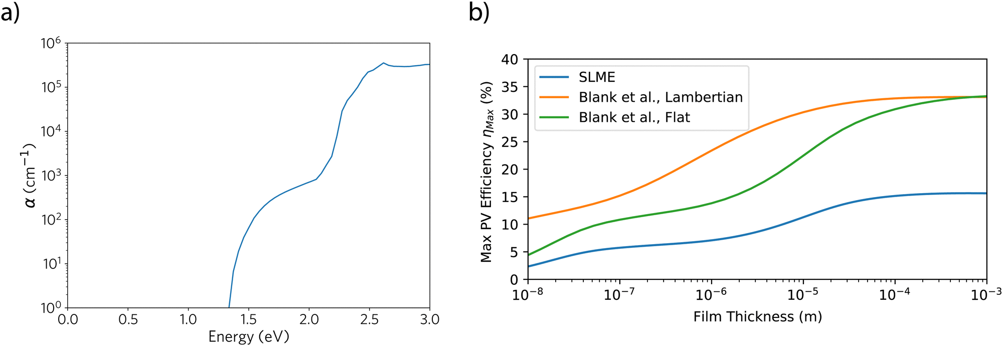
Fig. 6 shows the calculated theoretical absorption coefficient with HSE06: while there is a weak onset of absorption from above the direct transition at 1.3 eV (in the absence of electron–phonon coupling, indirect transitions are unavailable), strong absorption (>1 × 105 cm−1) occurs only above 2 eV – this is due to the first direct transition at Γ being parity-forbidden. The stronger onset is likely correspondent with the availability of either the transition at Γ from the second set of bands below the valence band (VBM-2) to the conduction band (2.42 eV), or the direct transition at E (2.21 eV). The HSE06 + SOC calculation shows similar results (ESI,† Fig. S7), with the spectrum negligibly red-shifted. This poor absorptivity in the red-visible region of the spectrum is promising for the material as a IR-transparent conductor, while less so for any intended use as a p-type solar absorber. The observed two-step theoretical absorption does mostly compare with the recorded transmittance data from Gao et al., in which the majority of transmittance loss occurs below 1000 nm, with complete absorption by 600 nm. To fully establish the unsuitability of LaSe2 as a solar absorber, we may use the SLME metric,38 and the method of Blank et al.39 both of which can be useful to compare the effectiveness of different thin-film materials as candidate photovoltaic absorbers: the percentage efficiencies for these two methods are given in Table 3, while their dependence on film thickness is given in Fig. 6(b). We can see that the different metrics give quite widely varying results for LaSe2 for a film thickness of 1 μm – the large difference between indirect and direct allowed transitions means that the SLME is very low, comparable to a very low internal quantum efficiency (Qi) in the Blank metric. Even with ideal radiative behaviour (Qi = 1), the modelled efficiencies are still low if the front surface of the material is modelled as perfectly flat, though, due to the high theoretical refractive index (∼3), and could be much improved if the surface is a Lambertian scatterer. The efficiencies improve when larger film thicknesses are considered, however given these thicknesses become comparable to those of silicon-based devices, the practical usage of less abundant and minimally developed LaSe2 becomes unlikely. Correspondingly, at low film thicknesses, the prediction of poor PV behaviour can be considered positive for the material's usage as an IR-transparent hole conductor instead. In all, considering the poor absorptivity even once the direct transition is reached, and that the indirect gap will limit any open-circuit voltage, LaSe2 makes for a poor solar absorber candidate, and so from hereon we consider it solely as a transport material.
 | ||
| Fig. 6 Calculated HSE06 optical properties of LaSe2: (a) optical absorption coefficient; (b) predicted SLME38 and Blank et al.39 metrics given as a function of film thickness (Qi = 1 for Blank et al. metric). | ||
| Blank et al. metric Qi | HSE06 | HSE06 + SOC | ||
|---|---|---|---|---|
| Flat surface | Lambertian | Flat surface | Lambertian | |
| 1 | 13.83 | 23.39 | 14.00 | 24.03 |
| 10−2 | 11.13 | 20.19 | 11.26 | 20.73 |
| 10−4 | 9.71 | 17.65 | 9.81 | 18.11 |
| 10−6 | 8.30 | 15.13 | 8.38 | 15.51 |
| SLME | 7.09 | — | 7.30 | — |
Thus far, we have established that LaSe2 should possess reasonable transparency in the IR-region, particularly as a thin film where the impact of indirect transitions will be minimized, and low effective masses in two of three dimensions, but to further investigate its potential as a conductive material, we should attempt to predict its carrier transport properties. Many prior screening studies attempting to predict transport properties from ab initio electronic structure alone have been forced to rely on the constant relaxation time approximation in which all scattering mechanisms are combined into a single relaxation time, typically around 1 × 10⁻¹⁴ s for most semiconductors. The recent development of the AMSET code,46 however, allows studies to move beyond the constant RTA and calculate explicit scattering rates for individual processes from ab initio calculated parameters within the momentum relaxation time approximation, while not requiring the very large computational expense associated with the use of Wannier functions for explicit electron–phonon coupling calculations. Additionally, we may see how the deviations that LaSe2 exhibits from typical 3D semiconductor behaviour affect those scattering rates, as well as considering behaviour across the relevant density of states region, rather than just at the band edge, as given by the effective masses.
The calculated directionally-averaged transport properties for p-type conduction in LaSe2 are given in Fig. 7(a) – to maintain a rough parity with the experimentally achieved carrier concentrations of 1 × 1018 cm−3 to 1.4 × 1019 cm−3 and room-temperature measurements, we initially consider only carrier concentrations between 1 × 1018 cm−3 to 2 × 1019 cm−3 and temperatures between 200 to 500 (a wider range in both variables is considered in the ESI†). The mobility at a carrier concentration of 1.1× 1019 cm−3, separated along the Cartesian directions, is then given in Fig. 7(b). It is immediately evident that the anisotropy in the valence band dispersion has a substantial effect on the relative mobilities, and thus conductivities; at the depicted carrier concentration of 1.1 × 1019 cm−3, there is a 2 order of magnitude difference between the mobility predicted along y/z and along x, concomitant with the substantially larger effective mass along the corresponding reciprocal vector. The directionally-averaged mobility, and conductivity, is inevitably affected, and as such, at 300 K, and a carrier concentration of 1.1 × 1019 cm−3 we predict a mobility of 90.5 cm2 V−1s−1 and a resultant conductivity of 159.2 S cm−1 (though a mere 1.42 S cm−1 along the x direction alone). Comparing this to the experimentally achieved mobility of 2 cm−2 V−1s−1 and conductivity of 3.7 S cm−1,7 at a similar carrier concentration, the predicted averaged transport properties appear to be significantly overestimated. There are two key reasons for this discrepancy: firstly, the AMSET model does not include deviations from single-crystalline behaviour – particularly the lack of grain boundary scattering or the effect of non-ionized film defects (point or extended) acting as traps, rather than the intended shallow acceptor states – both of these effects will mean that the experimental mobility and conductivity will inevitably be lower. Given the very limited number of prior studies on the material, there could be potential for substantial improvements in film quality, trap concentrations or grain size that could increase hole conductivity. Secondly, the severe anisotropy of the transport properties means that should the growth of the film result in a preferred orientation that emphasises (100), there could be a significant reduction in mobility. Careful control of film growth and orientation to encourage the more strongly conductive facets on the substrate could lead to improved carrier transport and device performance, as seen in the optimization of target properties other anisotropic chalcogenides such as reducing recombination centres in Sb2Se354 and driving the thermoelectric capability of thin-film SnSe.55
 | ||
| Fig. 7 Transport properties of LaSe2, calculated using the HSE06 functional (interpolated 43 × 85 × 43 mesh): (a) predicted p-type conductivity, Seebeck coefficient and electronic thermal conductivity across a range of experimentally-obtained carrier concentrations (plotted using the thermoplotter package56); (b) predicted hole mobility, separated by Cartesian direction (due to the small distortion of the cell away from orthorhombic, x and z are only approximately aligned with a and c); (c) and (d) hole mobility separated by scattering mechanism (ADP: acoustic deformation potential scattering, POP: polar optical phonon scattering, IMP: ionized impurity scattering) at a carrier concentration of 1 × 1019 cm−3, and a temperature of 300 K respectively, plotted using the AMSET package.46 | ||
As part of this analysis, we can also consider the individual scattering mechanisms – the contributions of each scattering mechanism towards the overall mobility is displayed in Fig. 7(c) and (d), respectively dependent on temperature and carrier concentration. At low carrier concentrations and room temperature, scattering from polar optical phonons is clearly the dominant scattering process in LaSe2. This results from an overall low polar optical phonon frequency of 3.1 THz; despite the relative chemical hardness of La, the high atomic masses of both elements as well as the soft Se–Se bonding lead to overall low phonon frequencies, as demonstrated earlier in the calculated phonon dispersion curve. This behaviour is also replicated regardless of crystal dimension, and does align with recent work by Ganose et al. that suggests that polar optical phonon scattering controls the temperature dependence in many more compounds than previously thought57 – the acoustic deformation potential, by contrast, appears to remain a minor contribution regardless of carrier concentration. Towards the upper end of the experimentally achieved carrier concentrations, the polar optical phonon scattering rates lower, but the importance of ionized impurity scattering increases; overall, though, the balance between these two factors means that the mobility is expected to moderately increase between 1 × 1018 cm−3 to 1 × 1019 cm−3, a trend somewhat replicated in the mobilities measured by Gao et al. (although the sharp increase in mobility for the film annealed at 900 °C, with lower carrier concentration, cannot be explained).7
Thus far, we have only considered the carrier concentrations accessed experimentally so far which, it must be noted, are for intrinsic LaSe2 alone – higher carrier concentrations may be possible with extrinsic doping, and so to consider the future potential of the material, we may also consider how the predicted transport behaviour varies under a wider range of carrier concentrations. The calculated transport properties for LaSe2 between 1 × 1016 cm−3 to 1 × 1021 cm−3 and 300 K to 700 K are plotted in ESI,† Fig. S9, and demonstrate that even higher p-type conductivities could be available (approaching 1 × 10⁴ S cm−1) should LaSe2 be extrinsically doped. Additionally, with reasonable Seebeck coefficients and electronic thermal conductivities, LaSe2 may be possibly considered as a candidate low-temperature p-type thermoelectric, though a full assessment would require detailed study of the lattice thermal conductivity and defect chemistry that is beyond the scope of this initial study of the electronic and optical properties. Nevertheless, through these results we have been able to demonstrate that LaSe2 shows potential as an IR-transparent p-type conductor in two dimensions.
4 Conclusion
In conclusion, electronic and optical properties of LaSe2 have been calculated using hybrid DFT, with confirmation that the ground state structure is monoclinic, not tetragonal, through vibrational calculations of both structures. We find that the electronic structure of LaSe2 is controlled by the distortion of the Se− layer to form Se–Se dimers leading to highly anisotropic band dispersion at the valence band maximum. The indirect band gap of LaSe2 is found to be 0.76 eV and 0.92 eV with HSE06 and QSGŴ respectively, but it is also found that the optical absorption of thin films is likely to be suppressed into visible-light frequencies due to multiple forbidden direct transitions, explaining previous experimental results. Finally, we perform transport calculations that demonstrate LaSe2 has high theoretically achievable p-type mobilities and conductivities at previously-achieved carrier concentrations, though with a 2 order-of-magnitude difference between the in-layer and out of layer directions. These results suggest that, with further development, LaSe2 could be an excellent candidate for an IR-transparent p-type 2D conductive material.Conflicts of interest
There are no conflicts to declare.Acknowledgements
The authors would like to thank Dr Katarina Brlec, Dr Kieran Spooner, Dr Alex Ganose, Prof. Claire Carmalt and Prof. David Scanlon for useful discussions. CNS is grateful to the Department of Chemistry at UCL and the Ramsay Memorial Fellowship Trust for the funding of a Ramsay fellowship. The use of the UCL Myriad and Kathleen High Performance Computing Facilities (Myriad@UCL and Kathleen@UCL) are acknowledged in the production of this work. Computational work was also performed on the ARCHER2 UK National Supercomputing Service, via our membership of the UK's HEC Materials Chemistry Consortium, funded by EPSRC (EP/R029431, EP/X035859).Notes and references
- S. A. Ring and M. Tecotzky, Inorg. Chem., 1964, 3, 182–185 CrossRef CAS.
- Y. Yanagisawa and S. Kume, Mater. Res. Bull., 1973, 8, 1241–1245 CrossRef CAS.
- I. Vasilyeva and S. Belaya, J. Solid State Chem., 1999, 146, 211–216 CrossRef CAS.
- B. L. Rolland, P. Molinié, P. Colombet and P. McMillan, J. Solid State Chem., 1994, 113, 312–319 CrossRef CAS.
- F. Holtzberg, P. E. Seiden and S. von Molnar, Phys. Rev., 1968, 168, 408–412 CrossRef CAS.
- G. Gao, L. Yang, B. Dai, S. Guo, Z. Yang, P. Wang, F. Geng, L. Xu, F. Xia, P. Min and J. Zhu, Mater. Lett., 2019, 254, 250–253 CrossRef CAS.
- G. Gao, L. Tong, L. Yang, C. Sun, L. Xu, F. Xia, F. Geng, J. Xue, H. Gong and J. Zhu, Appl. Phys. Lett., 2021, 118, 261602 CrossRef CAS.
- J. Willis and D. O. Scanlon, J. Mater. Chem. C, 2021, 9, 11995–12009 RSC.
- H. Kawazoe, M. Yasukawa, H. Hyodo, M. Kurita, H. Yanagi and H. Hosono, Nature, 1997, 389, 939–942 CrossRef CAS.
- M. N. Huda, Y. Yan, A. Walsh, S.-H. Wei and M. M. Al-Jassim, Phys. Rev. B: Condens. Matter Mater. Phys., 2009, 80, 035205 CrossRef.
- J. B. Varley, A. Miglio, V.-A. Ha, M. J. van Setten, G.-M. Rignanese and G. Hautier, Chem. Mater., 2017, 29, 2568–2573 CrossRef CAS.
- G. Brunin, F. Ricci, V.-A. Ha, G.-M. Rignanese and G. Hautier, npj Comput. Mater., 2019, 5, 63 CrossRef.
- A. Grzechnik, J. Z. Zheng, D. Wright, W. T. Petuskey and P. F. McMillan, J. Phys. Chem. Solids, 1996, 57, 1625–1634 CrossRef CAS.
- F. Bertolotti, A. V. Shishkina, A. Forni, G. Gervasio, A. I. Stash and V. G. Tsirelson, Cryst. Growth Des., 2014, 14, 3587–3595 CrossRef CAS.
- S. Bénazeth, J. Dugué, D. Carré, M. Guittard and J. Flahaut, The Rare Earths in Modern Science and Technology, Springer, US, 1980, pp. 223–224 Search PubMed.
- E. I. Yarembash, E. S. Vigileva, R. R. Kagramanova and L. K. Kravchen-Ko, Inorg. Mater., 1969, 5, 217–220 Search PubMed.
- M. Grupe and W. Urland, J. Less-Common Met., 1991, 170, 271–275 CrossRef CAS.
- S. Sasaki, D. Driss, E. Grange, J.-Y. Mevellec, M. T. Caldes, C. Guillot-Deudon, S. Cadars, B. Corraze, E. Janod, S. Jobic and L. Cario, Angew. Chem., Int. Ed., 2018, 57, 13618–13623 CrossRef CAS PubMed.
- R. Atif, A. Zarkov, D. R. C. Asuigui, P. Glaser, O. Stewart and S. L. Stoll, Chem. Mater., 2019, 31, 7779–7789 CrossRef CAS.
- J. H. Chen and P. K. Dorhout, J. Solid State Chem., 1995, 117, 318–322 CrossRef CAS.
- A. Eliseev and G. Kuz’micheva, Dokl. Akad. Nauk SSSR, 1979, 246, 1162–1165 CAS.
- A. Eliseev, V. Tolstova and G. Kuz’micheva, Zh. Neorg. Khim., 1978, 23, 3171–3180 CAS.
- J. Dugué, D. Carré and M. Guittard, Acta Crystallogr., Sect. B: Struct. Crystallogr. Cryst. Chem., 1978, 34, 403–406 CrossRef.
- T. Schleid, P. Lauxmann, C. Bartschb and T. Doert, Z. Naturforsch. B, 2009, 64, 189–196 CrossRef CAS.
- A. W. Webb and H. T. Hall, Inorg. Chem., 1970, 9, 843–847 CrossRef CAS.
- G. Kresse and J. Hafner, Phys. Rev. B: Condens. Matter Mater. Phys., 1993, 47, 558–561 CrossRef CAS PubMed.
- G. Kresse and J. Hafner, Phys. Rev. B: Condens. Matter Mater. Phys., 1994, 49, 14251–14269 CrossRef CAS PubMed.
- G. Kresse and J. Furthmüller, Phys. Rev. B: Condens. Matter Mater. Phys., 1996, 54, 11169–11186 CrossRef CAS PubMed.
- G. Kresse and J. Furthmüller, Comput. Mater. Sci., 1996, 6, 15–50 CrossRef CAS.
- P. Blochl, Phys. Rev. B: Condens. Matter Mater. Phys., 1994, 50, 17953–17979 CrossRef PubMed.
- J. Perdew, K. Burke and M. Ernzerhof, Phys. Rev. Lett., 1996, 77, 3865–3868 CrossRef CAS PubMed.
- J. P. Perdew, A. Ruzsinszky, G. I. Csonka, O. A. Vydrov, G. E. Scuseria, L. A. Constantin, X. Zhou and K. Burke, Phys. Rev. Lett., 2008, 100, 136406 CrossRef PubMed.
- J. Heyd, G. E. Scuseria and M. Ernzerhof, J. Chem. Phys., 2003, 118, 8207–8215 CrossRef CAS.
- A. V. Krukau, O. A. Vydrov, A. F. Izmaylov and G. E. Scuseria, J. Chem. Phys., 2006, 125, 224106 CrossRef PubMed.
- C. Adamo and V. Barone, J. Chem. Phys., 1999, 110, 6158 CrossRef CAS.
- A. Togo and I. Tanaka, Scr. Mater., 2015, 108, 1–5 CrossRef CAS.
- J. M. Skelton, L. A. Burton, A. J. Jackson, F. Oba, S. C. Parker and A. Walsh, Phys. Chem. Chem. Phys., 2017, 19, 12452–12465 RSC.
- L. Yu and A. Zunger, Phys. Rev. Lett., 2012, 108, 068701 CrossRef PubMed.
- B. Blank, T. Kirchartz, S. Lany and U. Rau, Phys. Rev. Appl., 2017, 8, 024032 CrossRef.
- A. M. Ganose, A. J. Jackson and D. O. Scanlon, J. Open Source Softw., 2018, 3, 717 CrossRef.
- T. Kotani, M. van Schilfgaarde and S. V. Faleev, Phys. Rev. B: Condens. Matter Mater. Phys., 2007, 76, 165106 CrossRef.
- D. Pashov, S. Acharya, W. R. Lambrecht, J. Jackson, K. D. Belashchenko, A. Chantis, F. Jamet and M. van Schilfgaarde, Comput. Phys. Commun., 2020, 249, 107065 CrossRef CAS.
- B. Cunningham, M. Grüning, P. Azarhoosh, D. Pashov and M. van Schilfgaarde, Phys. Rev. Mater., 2018, 2, 034603 CrossRef CAS.
- J. Buckeridge and D. O. Scanlon, Phys. Rev. Mater., 2019, 3, 051601 CrossRef CAS.
- P. A. E. Murgatroyd, M. J. Smiles, C. N. Savory, T. P. Shalvey, J. E. N. Swallow, N. Fleck, C. M. Robertson, F. Jäckel, J. Alaria, J. D. Major, D. O. Scanlon and T. D. Veal, Chem. Mater., 2020, 32, 3245–3253 CrossRef CAS PubMed.
- A. M. Ganose, J. Park, A. Faghaninia, R. Woods-Robinson, K. A. Persson and A. Jain, Nat. Commun., 2021, 12, 2222 CrossRef CAS PubMed.
- J. M. Skelton, D. Tiana, S. C. Parker, A. Togo, I. Tanaka and A. Walsh, J. Chem. Phys., 2015, 143, 064710 CrossRef PubMed.
- T. J. Whittles, T. D. Veal, C. N. Savory, P. J. Yates, P. A. E. Murgatroyd, J. T. Gibbon, M. Birkett, R. J. Potter, J. D. Major, K. Durose, D. O. Scanlon and V. R. Dhanak, ACS Appl. Mater. Interfaces, 2019, 11, 27033–27047 CrossRef CAS PubMed.
- N. Fleck, T. D. C. Hobson, C. N. Savory, J. Buckeridge, T. D. Veal, M. R. Correia, D. O. Scanlon, K. Durose and F. Jäckel, J. Mater. Chem. A, 2020, 8, 8337–8344 RSC.
- Y. Kang, Y. Youn, S. Han, J. Park and C.-S. Oh, Chem. Mater., 2019, 31, 4072–4080 CrossRef CAS.
- J. Kangsabanik, M. K. Svendsen, A. Taghizadeh, A. Crovetto and K. S. Thygesen, J. Am. Chem. Soc., 2022, 144, 19872–19883 CrossRef CAS PubMed.
- L. J. Phillips, C. N. Savory, O. S. Hutter, P. J. Yates, H. Shiel, S. Mariotti, L. Bowen, M. Birkett, K. Durose, D. O. Scanlon and J. D. Major, IEEE J. Photovolt., 2018, 9, 544–551 Search PubMed.
- Y.-T. Huang, S. R. Kavanagh, M. Righetto, M. Rusu, I. Levine, T. Unold, S. J. Zelewski, A. J. Sneyd, K. Zhang, L. Dai, A. J. Britton, J. Ye, J. Julin, M. Napari, Z. Zhang, J. Xiao, M. Laitinen, L. Torrente-Murciano, S. D. Stranks, A. Rao, L. M. Herz, D. O. Scanlon, A. Walsh and R. L. Z. Hoye, Nat. Commun., 2022, 13, 4960 CrossRef CAS PubMed.
- Y. Zhou, L. Wang, S. Chen, S. Qin, X. Liu, J. Chen, D.-J. Xue, M. Luo, Y. Cao, Y. Cheng, E. H. Sargent and J. Tang, Nat. Photonics, 2015, 9, 409–415 CrossRef CAS.
- S. H. Heo, S. Jo, H. S. Kim, G. Choi, J. Y. Song, J.-Y. Kang, N.-J. Park, H. W. Ban, F. Kim, H. Jeong, J. Jung, J. Jang, W. B. Lee, H. Shin and J. S. Son, Nat. Commun., 2019, 10, 864 CrossRef PubMed.
- K. B. Spooner, M. Einhorn, D. W. Davies and D. O. Scanlon, J. Open Source Softw., 2024, 9, 6340 CrossRef.
- A. M. Ganose, J. Park and A. Jain, The temperature-dependence of carrier mobility is not a reliable indicator of the dominant scattering mechanism, arXiv, 2210.01746, 2022, [cond-mat.mtrl-sci].
Footnotes |
| † Electronic supplementary information (ESI) available: Comparisons of vibrational spectra to experimental literature, analysis of valence band maxima and conduction band maximum, extended plots of band structure and electronic transport properties. Calculation data is included in a github repository (https://github.com/cnsavory/LaSe2). See DOI: https://doi.org/10.1039/d3tc02833j |
| ‡ These authors contributed equally to this work. |
| This journal is © The Royal Society of Chemistry 2024 |