
 Open Access Article
 This Open Access Article is licensed under a Creative Commons Attribution-Non Commercial 3.0 Unported Licence
Fast fabrication of μm-thick perovskite films by using a one-step doctor-blade coating method for direct X-ray detectors†
Kuo-Wei
Huang
a,
Ming-Hsien
Li
b,
Yen-Ting
Chen
a,
Zi-Xiang
Wen
a,
Chen-Fu
Lin
a and
Peter
Chen
 *acd
*acd
aDepartment of Photonics, National Cheng Kung University, Tainan 70101, Taiwan. E-mail: petercyc@ncku.edu.tw
bDepartment of Applied Materials and Optoelectronic Engineering, National Chi Nan University, Nantou, 54561, Taiwan
cCore Facility Center (CFC), National Cheng Kung University, Tainan, 70101, Taiwan
dHierarchical Green-Energy Materials (Hi-GEM) Research Center, National Cheng Kung University, Tainan 70101, Taiwan
First published on 20th December 2023
Abstract
Deposition of large-area perovskite films for direct X-ray detectors under ambient conditions is highly desirable for commercial application. In this work, we employ a one-step doctor-blade coating method to prepare a perovskite film with the advantages of rapid fabrication, easy scalability, and raw material savings. We incorporate a high content of 20-wt% crown ether, namely 18-crown ether-6 (18C6), into the perovskite precursor solution to prepare a μm-thick perovskite film, which effectively attenuates the X-ray irradiation. The large cyclic structure of 18C6 bonding with the DMSO solvent and solutes via the hydrogen and van der Waals forces increases the viscosity of the precursor solution from 3.4 mPa s (0-wt% 18C6) to 41.3 mPa s (20-wt% 18C6). A continuous, compact, and uniform perovskite thick film with a thickness of 6.2 μm is fabricated by the doctor-blade coating in just 10 seconds. The direct X-ray detectors based on the doctor-bladed perovskite thick film achieve a dark current density of 1.6 nA cm−2 under an electric field of 1/20 of that required for the commercial a-Se-based X-ray detector. The device sensitivity reaches 33.51 μC Gyair−1 cm−2, and the limit of detection is determined to be 70.17 μGyair s−1. Our study paves a way toward industrialization with the merits of scalable, fast and easy production, and low-cost X-ray detectors.
1. Introduction
Halide perovskite-based solar cells (PSCs) have attracted enormous attention due to their boosting power conversion efficiency (PCE).1–4 The record PCE of PSCs is certified to be over 26%.5 Besides the PSCs, halide perovskites have been applied in various devices, such as light-emitting diodes (LEDs),6 memory,7 lasers,8 light detection and ranging (LiDAR),9,10 X-ray detectors and so on. A halide perovskite has a high attenuation coefficient (α) for the X-ray irradiation due to its composition with large atomic-number (Z) elements, such as Cs (55), Pb (82), Br (35), I (53) and so on.11 Compared with the commonly used X-ray-sensitive semiconductors (like Si,12,13 a-Se,14,15 CdTe,16,17 PbI2,18,19 and HgI220,21), the halide perovskite demonstrates a larger charge mobility-lifetime (μτ) product, a lower defect density, and a lower carrier recombination.22 Moreover, the large resistivity of the perovskite film can achieve a low dark current density for the X-ray detectors, which is beneficial for enhancing the signal-to-noise (S/N) ratio for sensing high energy radiation, specifically gamma-rays and X-rays.23–28 Unlike the expensive vacuum process for producing the aforementioned semiconductor materials, the halide perovskite film can be fabricated by a low-cost solution process in an ambient environment.29 Although the X-ray detector using a single-crystal perovskite delivered a remarkable performance due to its low defect density and low carrier recombination,30 the harsh synthesis conditions, time-consuming synthesis, and limited crystal size hinder the real application of single-crystal perovskites to integrate with the thin-film transistor (TFT) panel array for direct X-ray imaging.Currently, several up-scale fabrication approaches, such as spray coating,31–35 slot-die coating,36–41 doctor-blade coating,42–46 air knife,47 and inkjet printing,48–50 are implemented for the large-area PSCs. In addition, doctor-blade coating,51,52 spray coating,53 inkjet printing,54 tablet pressing14 and bar coating55 are conducted for the fabrication of large-area perovskite-based X-ray detectors. Among these up-scale methods, the doctor-blade coating is a simple, versatile, and continuous fabrication process to produce a large-area perovskite film with high material utilization.42 Usually, the thickness of the perovskite film for the X-ray detection must be larger than 50 μm, which is much thicker than the perovskite active layer in the PSCs (<1 μm). The experimental conditions and parameters for fabrication of perovskite thick films are completely different from that for fabrication of perovskite thin films. Spray coating is a facile method to fabricate perovskite thick films; however, it usually takes at least 3 or 4 h to reach a thickness of over 50 μm. Even though the processing period for spray-coated thick films is substantially shortened compared to that for vacuum-processed a-Se (at less 10 h),56 the processing period for fabrication of large-area perovskite films should be further reduced.
Doctor-blade coating technology is one of the great potential candidates to reduce the processing period. Therefore, although there are many literature studies on the fabrication of perovskite solar cells by doctor-blade coating,57–59 there are still very few works involving the use of doctor-blade coating for the perovskite-based X-ray detectors. At first, Kim et al. used a polyimide/methylammonium lead iodide (MAPbI3) composite to fabricate an 830-μm-thick perovskite film by doctor-blade coating. Additional two interlayers of polymer/perovskite composites provide conformal interfaces between the perovskite films and the electrodes that can regulate dark currents and temporal charge carrier transportation for the X-ray detectors. The as-fabricated devices exhibited a sensitivity of 11 μC mGyair−1 cm−2.51 Dong et al. employed non-toxic solvent of methylamine acetate (MAAc) and additive of methylamine chloride (MACl) to fabricate a methylammonium bismuth iodide (MA3Bi2I9) perovskite for the X-ray detector by doctor-blade coating. The corresponding X-ray detector exhibited a sensitivity of 100.16 μC Gyair−1 cm−2 with a limit of detection (LoD) of 98.4 nGyair s−1. For increasing the thickness of perovskite detection films, the doctor-blade coating was repeated twice, thereby increasing the period of fabrication of perovskite films.52
The fabrication of perovskite films with thicknesses in the range of hundreds of micrometers is critical to significantly attenuating X-rays, thereby improving X-ray detection. However, employing a doctor-blade coating technique to prepare such thick perovskite films presents certain challenges. First, in typical practice, the perovskite precursor is doctor-bladed onto a substrate that has been heated to a specific temperature. The heating temperature can rapidly evaporate the solvent from the perovskite precursor loaded on the preheated substrate and the bladed perovskite wet film. Moreover, the solvent evaporation and perovskite condensation can be balanced by the heating temperature which allows the formation of a stable wet film with a suitable viscosity that can yield a smooth surface. When aiming to coat a perovskite film with a thickness in the hundreds of micrometers, it becomes necessary to increase the amount of perovskite precursor loaded on the substrate while simultaneously reducing the blading rate. This adjustment facilitates achieving the desired thickness of the perovskite film after the doctor-blade coating. However, this also means that the increasing amount of perovskite precursor on the substrate can solidify quickly, potentially hindering the blade-coating process. Secondly, during the doctor-blade coating, the temperature near the surface of the thick perovskite film is significantly lower than that near the substrate. This temperature gradient can lead to convection within the perovskite wet film, potentially impacting the growth process and morphology of the perovskite film. Therefore, well-controlled preparation conditions for these hundreds-of-micrometer-thick perovskite films are essential, including optimizing the perovskite precursor loading rate, substrate temperature, and blading rate.
Recently, we have introduced an eco-friendly solvent system composed of γ-butyrolactone (GBL), dimethyl sulfoxide (DMSO), and isopropanol (IPA) for the ambient-processed perovskite film via doctor-blade coating. Adding IPA in the precursor facilitates the DMSO evaporation, and suppresses the DMSO–perovskite intermediate phase and the trap density in the perovskite film.60 Moreover, we introduce 18-crown ether-6 (abbreviated as 18C6) as a crystallization control agent in the doctor-bladed perovskite film to effectively improve the film uniformity along with the performance of PSC.59 Based on these works, in this study, we add 18C6 in the perovskite precursor to increase its viscosity for the aim of increasing the perovskite film thickness via doctor-blade coating. A thick methylammonium lead bromide (MAPbBr3) perovskite film with a thickness of 6.2 μm is successfully fabricated by one-step doctor-blade coating under an ambient environment. This process just takes only ten seconds to fully demonstrate the advantages of blade coating due to its time-saving process. This doctor-blade coating MAPbBr3 perovskite film is further applied for the direct X-ray detector with a device architecture of FTO/TiO2/MAPbBr3/Au. The X-ray detector presents a sensitivity of 33.51 μC Gyair−1 cm−2 and a LoD of 21.31 μGyair s−1, when the device is exposed to an X-ray tube operated at 90 kVp. The performance of a MAPbBr3-based X-ray detector is greater than that of the a-Se-based counterpart, which is commonly used in the field of medical X-ray testing. The one-step doctor-blade coating for perovskite-based X-ray detectors is much faster and simpler than the previous works using doctor-blade coating. This time-efficient fabrication of a perovskite-based X-ray detector with acceptable sensitivity is critical for commercial applications.
2. Results and discussion
To achieve a great performance for the direct X-ray detector, we must first understand the factors affecting the X-ray detection. Eqn (1) presents the relationship between the X-ray attenuation ratio and the thickness of the photoactive material:| ε = 1 − exp(−αL), | (1) |
During the doctor-blade coating process, the substrate is heated to facilitate solvent evaporation from the doctor-bladed wet perovskite film. The evaporation of the solvent leads to the oversaturation of the perovskite, inducing perovskite growth. As the concentration of the perovskite precursor increases, the rate of oversaturation becomes faster, resulting in an accelerated perovskite growth rate. This rapid growth rate causes the formation of square-shaped domains. Consequently, the square-shaped perovskite domains grow larger with increasing concentration, leading to an uneven surface morphology of the doctor-bladed perovskite films. The high surface roughness of the perovskite films hinders the full coverage of the top electrode on the surface of the perovskite films, resulting in an increased dark current and a noticeable decrease in the charge carrier transport efficiency. In the subsequent experiments, a MAPbBr3 precursor solution with a concentration of 2.0 M is carried out to produce the perovskite film.
To enhance the X-ray attenuation ratio of the perovskite photoactive film, it is necessary to increase the thickness of the perovskite film. In order to demonstrate the advantages of the blade-coating process, which is a facile and a fast fabrication process, we first apply a multiple doctor-blade coating approach to increase the thickness of perovskite films. As shown in Fig. 1, when a single-layer MAPbBr3 film was prepared using the blade-coating method, vertically oriented perovskite domains (Fig. 1a) are well-arranged laterally to create a compact and crack-free perovskite film. When a second layer is blade-coated on the top of the first layer, as shown in Fig. 1b, a distinct interfacial boundary is observed between the first and second doctor-bladed perovskite layers, and some debris, which is presumably the PbBr2, are detected near the interface. During the blade coating of second perovskite precursor solution onto the surface of the first-layer perovskite film, the precursor solution dissolves the surface of underlying perovskite film. Due to a slightly lower surface temperature of the first-layer perovskite film compared to the underlying heating plate, the re-crystallization process after the dissolution near the interface proceeds at a slow rate. This preferentially led to the formation of PbX2 through the binding of coordinated lead polyhalogeno ([PbX3]−, [PbX4]2−, [PbX5]3−, and [PbX6]4−), rather than the preferential formation of perovskite structure by binding with MA+ cations.61,62 Therefore, a noticeable residual of PbBr2 debris appears at the interfacial boundary between the first- and second-deposited perovskite layers. Additionally, clear cracks are observed within the first-layer film, suggesting that the solvent of the perovskite precursor during second doctor-blade coating infiltrates into the first-layer perovskite film. The penetration of solvent into the first-deposited perovskite film disrupts the continuity and induces cracks in the first-layer perovskite film. It is noted that the morphology of the upper layer corresponding to the second-deposition perovskite layer remains compact and crack-free. Fig. 1c shows the cross-sectional SEM image of the perovskite film after stacking three-layer of doctor-bladed perovskite and reveals that the solvent, which constituted nearly 90% of the precursor solution, greatly changes the morphology of pre-deposited perovskite layers. The uppermost layer of doctor-bladed wet film, in contact with air, would rapidly initiate the perovskite nucleation. The solvent of next deposition concurrently dissolves the pre-deposited perovskite layers and remains in the dissolved perovskite layer. When the residual solvent vaporized during heating, the evaporating solvent could cause surface disruptions of the perovskite film, leading to apparent cracks in the perovskite thick film. Moreover, a great temperature gradient across the perovskite wet film in a large thickness may result in different growth rates of perovskite crystals in the surface and the bulk of wet films. Although the doctor-bladed perovskite after triple deposition achieves a thickness of 24.58 μm, a rough and a loose perovskite film results in an extremely high dark current to mA for the X-ray detector due to the direct contact between the top and bottom electrodes and a low charge carrier transport capability, which is unfavorable for the X-ray detection.
 | ||
| Fig. 1 Cross-sectional SEM images of MAPbBr3 perovskite films with a concentration of 2.0 M doctor-bladed with (a) one time, (b) two times, and (c) three times. Cross-sectional SEM images of doctor-bladed MAPbBr3 perovskite films with a concentration of 2.0 M added with (d) 15, (e) 20, and (f) 25 wt% 18C6. | ||
To address the issue of insufficient film thickness via the one-step doctor-blade coating, for the first time, this study employs the addition of a high proportion of 18C6 in the perovskite precursor solution as a thickening agent for the doctor-bladed perovskite film. The molecular structure of 18C6 is presented in the inset in Fig. S2 (ESI†). The large cyclic structure of 18C6 creates spatial hindrance and impedes the flow between 18C6 molecules.63 Moreover, Fig. S2 (ESI†) compares the Raman spectra of the perovskite precursor with and without 20-wt% 18C6. Given that the solvent constitutes about 90% of the perovskite precursor, the majority of the signals correspond to the solvent. Despite the prevailing DMSO signal over the MAPbBr3 signal, we were still able to identify the C–N+ stretching of MAPbBr3 (at the wavenumber of 953 cm−1) from the background of the DMSO spectra.64 We observed that in the presence of 18C6, the C–N+ stretching signal exhibits a blue shift, moving from 953 to 966 cm−1. Typically, a blue shift in a signal arises from changes in the molecular structure or an increase in intermolecular interactions. Therefore, it can be speculated that the addition of 18C6 leads to the formation of hydrogen bonds or van der Waals forces with the MAPbBr3 perovskite, thereby causing the observed blue shift in the C–N+ stretching signal. The strong chelating 18C6 coordinates with the cations in the perovskite precursor via the hydrogen bonding and the van der Waals forces to increase the precursor viscosity. The chelating 18C6 molecules in the perovskite precursor could further render the aggregation via the electrostatic interaction and affect the viscosity of the precursor solution. The results reveal that the film thickness of the perovskite fabricated by one-step doctor-blade coating increases from 1.8 to 3.4 μm after adding 15 wt% of 18C6 to the MAPbBr3 precursor solution as seen in Fig. 1d.
It is observed that the average viscosity of the perovskite precursor solution, measured using a handheld viscometer (VL7-100B-d15, Rixen), gradually increases from 3.4 mPa s to 51.9 mPa s when the 2.0 M MAPbBr3 perovskite precursor is added with 18C6 from 0 to 30 wt%, as revealed in Fig. S3a (ESI†). An increased viscosity of perovskite precursor solution aids in retaining a high solid content of perovskite solute during the doctor-blade coating. Furthermore, when a 20 wt% 18C6 is added in the precursor solution, the perovskite film reaches a thickness of 6.2 μm as shown in Fig. 1e. The corresponding photo of the as-deposited perovskite film is shown in Fig. S3c (ESI†). The resultant perovskite thick film exhibits a continuous and a uniform film surface without macro cracks as seen in Fig. 1e. In contrast, the perovskite film prepared by a spray coating method often encounters issues with an uneven film surface.65,66 It is noted that the one-step blade coating of a thick perovskite film with an area of 1 cm2 can be completed within ten seconds in this work. The result highlights the major advantages of the doctor-blade coating method for a fast production of perovskite thick films. The amount of 18C6 not only affects the precursor viscosity but also changes the solubility of the solute. When 25 wt% of 18C6 is added to the MAPbBr3 precursor solution, as shown in Fig. S3b (ESI†), a white turbidity, attributed to the formation of precipitates, is observed in the precursor solution. This turbidity persists even after heating the precursor overnight at a temperature of 90 °C, and the white turbidity is presumably due to the light scattering of large-sized aggregation, which is composed of the DMSO-coordinated and 18C6-coordinated complexes.67 When the MAPbBr3 precursor solution with 25-wt% 18C6 is doctor-bladed on the substrate, as shown in Fig. 1f, numerous μm-sized fractures appear in the resultant perovskite film, rendering the film discontinuous with many surface cracks. The corresponding photo of doctor-bladed perovskite film is presented in Fig. S4 (ESI†), indicating an incomplete coverage of perovskite film on the substrate. Adding excess amount of GBL solvent into the perovskite precursor solution effectively enhances the solubility and eliminates the white turbidity owing to the reduced complexation of metal cations with DMSO and 18C6 by GBL;68 however, excess of GBL significantly reduces the concentration of precursor solution and further reduces the thickness of the doctor-bladed perovskite film.
The photoluminescence (PL) spectra of doctor-bladed MAPbBr3 perovskite films with difference weight ratios of 18C6 are shown in Fig. 2a. It is found that addition of a high weight ratio of 18C6 doesn’t cause any shift in the PL emission peak resulting from perovskite films. Moreover, even though the perovskite film with 25 wt% 18C6 exhibits numerous cracks, the PL peak intensity still increases with the rising concentration of 18C6. This is attributed to the increased thickness of the perovskite film, varying from 1.86 μm (0 wt% 18C6) to 11.1 μm (25 wt% 18C6), as well as the improved crystallinity along the (003) facet (refer to Fig. 2b). Fig. 2b shows the X-ray diffraction (XRD) profiles of MAPbBr3 thick films prepared by doctor-blade coating with different weight ratios of 18C6. The XRD profiles reveal that the characteristic peaks at 15.12°, 21.37°, 26.23°, 30.3°, 33.97°, 37.35°, 43.4°, and 46.08° correspond well to the (001), (110), (111), (002), (210), (211), (220), and (003) facets of the MAPbBr3 perovskite, respectively. The MAPbBr3 perovskite film without adding 18C6 presents a preferred orientation along the (002) facet. Notably, after adding 18C6 in the doctor-bladed perovskite film, the resultant perovskite films exhibit a preferred orientation along the (003) facet. The perovskite film added with a 25 wt% 18C6 shows a higher XRD peak intensity along the (003) facet than the others. This suggests that addition of 18C6 in the perovskite precursor can assist the crystal growth along the preferred orientation of the (003) facet. The enhanced XRD intensity along the (003) facet may be attributed to the molecular interactions between 18C6 and the perovskite cations, possibly through the hydrogen bonding or non-covalent bonding. The 18C6 molecules could create a spatial hindrance to restrict the growth direction of perovskite crystal along (001) and (002) facets. There is no noticeable shift on the characteristic XRD peaks of doctor-bladed perovskite films with different 18C6 contents, suggesting that 18C6 facilitates the perovskite crystallinity toward the preferred orientation instead of incorporating into the perovskite lattice structure.
 | ||
| Fig. 2 (a) PL spectra and (b) XRD profiles of perovskite films with different wt% of 18C6. | ||
The impact of different wt% of 18C6 on the photoresponse of direct X-ray detector is securitized. The device structure is based on the heterojunction architecture and is composed of a fluorine doped tin oxide coated glass (FTO) substrate, ultrathin TiO2 as blocking layer (b-TiO2) as electron transport layer (ETL), a perovskite active layer, and a gold (Au) electrode (denoted as FTO/b-TiO2/perovskite/Au). The measurement setup is illustrated in Fig. S4 (ESI†). The distance between the detector and the X-ray source is 15 cm. The dose rate of X-ray tube operated with different voltage and current is calibrated using a dose meter and summarized in Fig. S5 (ESI†). The active area of the perovskite-based X-ray detector is 1.5 cm2.
The current density–voltage (J–V) and current density–time (J–t) curves of the perovskite-based X-ray detector with 20 wt% 18C6 are shown in Fig. 3. The operating voltage and current for the X-ray tube is 90 kVp and 10 mA, respectively. Under an electric field of −0.5 V μm−1, as shown in Fig. 3a, the dark current density of the perovskite-based X-ray detector can reach −1.54 nA cm−2, which is the lowest reported value among the perovskite-based X-ray detectors using a photoactive thickness less than 50 μm.52 The doctor-bladed perovskite thick film with 20 wt% 18C6 exhibits a uniform and a compact film surface, which can effectively prevent the direct contact between the top Au electrode and the bottom FTO substrate and the leakage of dark current. By considering the difference between the photocurrent and dark current, the sensitivity of the X-ray detector is determined to be 9.6 μC Gyair−1 cm−2. Furthermore, from the J–t curves shown in Fig. 3b, when the device is biased at an external electric field of −0.5 V μm−1, the sensitivity is determined to be 10.89 μC Gyair−1 cm−2. On the other hand, the perovskite-based X-ray detector exhibits a dark current density of −1.6 nA cm−2, whose value is close to that of commercial a-Se-based X-ray detectors (0.45 nA cm−2). Due to the poor optoelectrical properties of a-Se, the a-Se-based X-ray detectors are usually biased at a higher electric field (10 V μm−1), which is 20 times higher than the electric field used in this study (−0.5 V μm−1). Such a high electric field applied in a-Se-based X-ray detectors would result in an excessive background noise in the 2D X-ray flat-panel imaging.
 | ||
| Fig. 3 (a) J–V curves and (b) J–t curves of MAPbBr3-based X-ray detector. The operating voltage and current of X-ray tube is 90 kVp and 10 mA, respectively. (c) J–V curves MAPbBr3-based X-ray detector under forward and reverse scan directions. | ||
In the previous published literature reports, it has been observed that the lowest current density in the J–V curves is not at zero bias voltage. This phenomenon is presumably attributed to the asymmetric band diagram design in the existing device structures, which often incorporate n-type semiconductors such as TiO2 or SnO2, but typically lack p-type semiconductors such as 2,2′,7,7′-tetrakis[N,N-di(4-methoxyphenyl)amino]-9,9′-spirobifluorene (Spiro-OMeTAD) or polymer poly[bis(4-phenyl)(2,4,6-trimethylphenyl)amine] (PTAA). This asymmetry in energy levels leads to different carrier extracting rates within the perovskite film, when the device is operated with forward and reverse scans, as shown in Fig. 3c. When a negative voltage is applied on the device, the applied electric field favors the carrier transport through the n-type semiconductor to be collected and the lowest dark current density occurs at a negative bias voltage of ∼−0.25 V. Conversely, when the electric field is unfavorable for carrier transport, the lowest dark current occurs at a positive bias voltage of ∼0.25 V.
As mentioned previously, increasing the perovskite film thickness can effectively enhance the X-ray attenuation ratio. We further explore the sensitivity of X-ray detectors with different film thicknesses and electric field as shown in Fig. 4. For the device with the doctor-bladed perovskite film added with 20 wt% 18C6 (the thickness of perovskite photoactive film is ∼6.2 μm), the sensitivity of X-ray detector increases with the increasing electric field. The maximum sensitivity of 33.51 μC Gyair−1 cm−2 is obtained for the device biased at an electric field of −0.9 V μm−1. The X-ray detector prepared by printing processes requires multiple folding of flexible X-ray detectors to achieve a comparable sensitivity of 25–35 μC Gyair−1 cm−2.69 Our study demonstrates a facile fabrication process for X-ray photodetector fabrication with a fast fabrication period. On the other hand, for the X-ray photodetector without adding 18C6 (the thickness of perovskite photoactive film is ∼2.5 μm), the maximum sensitivity of 4.33 μC Gyair−1 cm−2 is achieved under an electric field of −0.4 V μm−1. The device with a perovskite film with 15-wt% 18C6, whose thickness is ∼3.8 μm, delivers a maximum sensitivity of 16.33 μC Gyair−1 cm−2 under an electric field of −0.8 V μm−1. However, when the electric field continues to increase to −1.0 V μm−1, the sensitivity does not further improve. These findings indicate that film thickness proudly affects the X-ray attenuation ratio and the maximum sensitivity of the detector.
 | ||
| Fig. 4 Sensitivity of MAPbBr3-based X-ray detector with different wt% of 18C6 as a function of electric field. The operating voltage and current of X-ray tube is 90 kVp and 10 mA, respectively. | ||
Additionally, different operating voltages on the X-ray tube are used for different applications, such as using 60 kVp in non-destructive testing in industrial applications. We further investigate the effect of X-ray source operating voltages on the perovskite-based X-ray detector under a fixed operating current (10 mA) and an electric field (−0.9 V μm−1). The ΔJ–t curves (the difference between photocurrent and dark current as a function of time) of device irradiated with X-ray tube under different operated voltages are presented in Fig. 5a–e, and the relationship between sensitivity and operating voltage is summarized in Fig. 5f. The results indicate that a stable photocurrent can be rapidly achieved regardless of whether the X-ray tube is operated at a low operating voltage (e.g., Fig. 5a at 50 kVp) or a high operating voltage (e.g., Fig. 5e at 90 kVp). The ΔJ–t curves of perovskite-based X-ray detectors show a rapid response to the X-ray pulse irradiation with an illumination duration of 30 s. When the X-ray irradiation is turned off, the X-ray detector immediately delivers a current that is close to the value of the dark current, and no tailing or signal below the baseline is seen in the ΔJ–t curves. As shown in Fig. S6 (ESI†), the rise time (the time required for the photocurrent to change from 10% to 90% of the saturated photocurrent) and fall time (the time needed for the photocurrent to change from 90% back to 10% of the saturated photocurrent) of the as-fabricated device is approximately 20 and 10 ms, respectively. The overall response time of the device is about 30 ms. This fast photoresponse facilitates signal collection and processing without the need for additional signal normalization in the capacitors of lower readout panel during 2D imaging, thereby improving the imaging speed. The results demonstrate that the fabricated X-ray detector is a fast-response detector in response to the X-ray irradiation. The sensitivity of X-ray detectors under different operating voltages are presented in Table 1. It can be observed that the sensitivity increases with the operating voltage of the X-ray tube. When the X-ray tube operating voltage is increased, high-energy X-ray photons interact with the perovskite sensing film to enhance the number of photogenerated electrons. Under a sufficient external electric field, an increased number of carriers can be easily extracted, resulting in an increase in sensitivity.
 | ||
| Fig. 5 ΔJ–t curves of the MAPbBr3-based X-ray detector irradiated with an X-ray tube operated at a voltage of (a) 50, (b) 60, (c) 70, (d) 80, and (e) 90 kVp and a current of 10 mA. The electric field is −0.9 V μm−1. (f) The sensitivity of the MAPbBr3-based X-ray detector as a function of the operating voltage of the X-ray tube. | ||
| Operating voltage (kVp) | 50 | 60 | 70 | 80 | 90 |
|---|---|---|---|---|---|
| Sensitivity (μC Gyair−1 cm−2) | 10.89 | 20.21 | 22.26 | 26.55 | 33.51 |
To estimate the LoD of X-ray detectors, there are two main measurement methods in the existing literature reports. The first one involves the use of lead foil filters of varying thickness to attenuate the X-ray radiation from the X-ray source.66 By gradually increasing the filter thickness, the dose rate received by the X-ray detector is reduced. When the filter thickness reaches a certain level, the X-ray detector will no longer receive X-ray radiation. This method can help us to determine the LoD of X-ray detectors. The experimental results are shown in Fig. S7 (ESI†). For X-ray irradiation filtered with 0.3-mm-thick Pb foil, the device still presents a photocurrent in response to X-ray pulse irradiation (Porta 100HF). However, when the thickness of the Pb foil filter increased to 0.4 mm, negligible photocurrent is detected. Based on this method, the minimum LoD of device is calculated to be 76 μGyair s−1 (X-ray tube operated at 50 kVp). The second method involves linearly fitting the photocurrent density against the dose rate and the LoD can be estimated by the following eqn (2):70
| LoD = I/(A × S), | (2) |
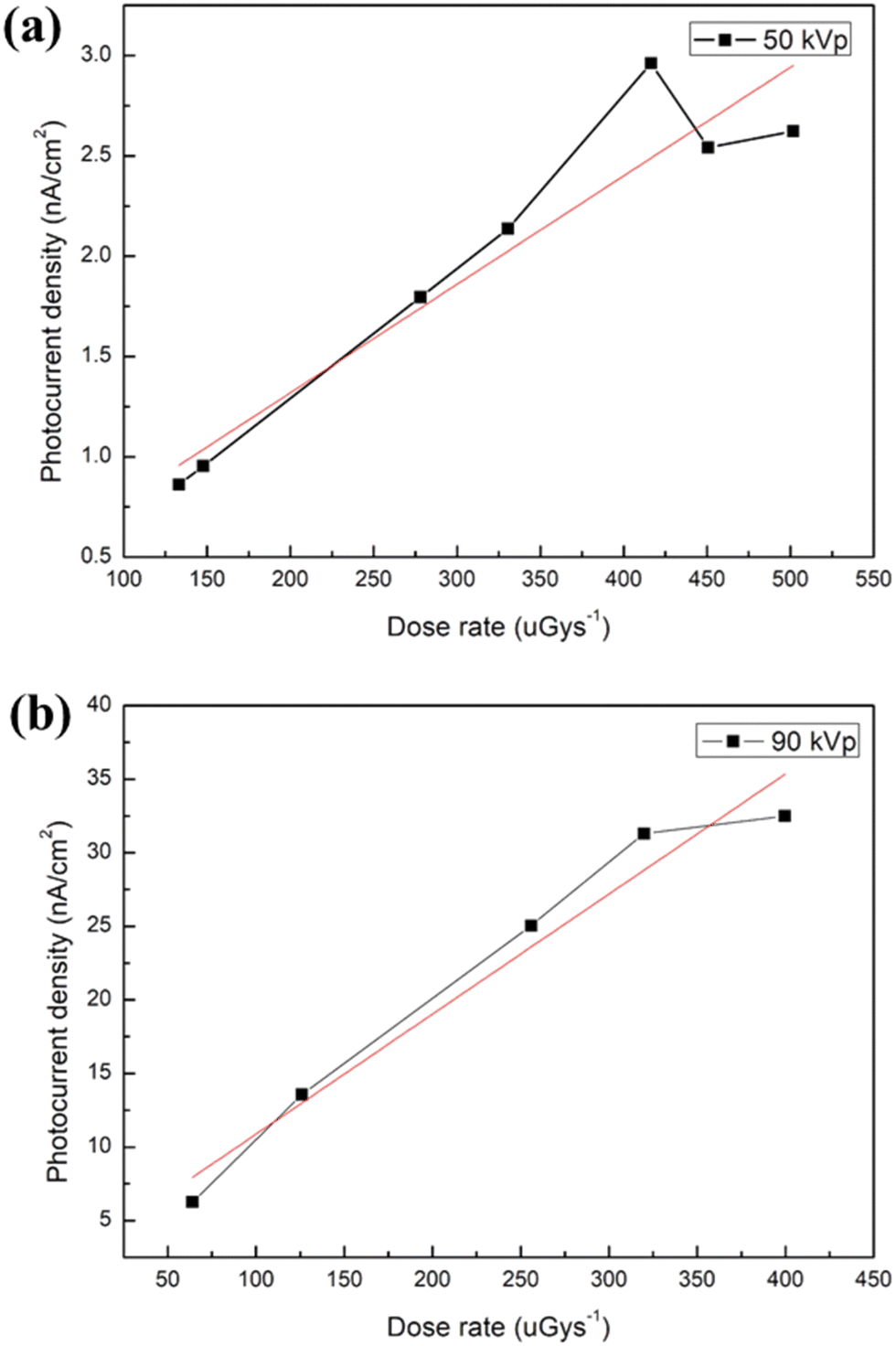 | ||
| Fig. 6 Photocurrent density of the MAPbBr3-based X-ray detector as a function of the dose rate for the X-ray tube operated at a voltage of (a) 50 and (b) 90 kVp. | ||
3. Conclusions
In summary, we incorporate a high content (20 wt%) of crown ether in the perovskite precursor to effectively increase its viscosity, which has a positive impact on the preparation of perovskite thick films by one-step doctor-blade coating. In a rapid fabrication, a continuous, a compact, and a uniformly deposited perovskite thick film with a thickness of 6.2 μm is prepared within just 10 seconds. The steric effect of crown ether promotes the preferential orientation of doctor-bladed perovskite along the (003) facet. A direct X-ray detector using a doctor-bladed perovskite thick film delivers a dark current density of 1.6 nA cm−2 under a 1/20 electric field of that required for commercial a-Se materials. Furthermore, the as-fabricated devices irradiated with X-ray pulse irradiation show a fast photoresponse, which is beneficial for the future X-ray 2D imaging applications. The perovskite-based X-ray detector exhibits a sensitivity of 33.51 μC Gyair−1 cm−2 with a LoD of 70.17 μGyair s−1. Our study demonstrates a facile, fast, and low-cost fabrication process for the up-scale perovskite-based X-ray detectors toward industrialization.Conflicts of interest
There are no conflicts to declare.Acknowledgements
The authors are grateful for the research grant from the Ministry of Science and Technology of Taiwan (MOST 111-2113-M-006-009, and MOST 111-2221-E-006-061-MY2) and the National Science and Technology Council of Taiwan (NSTC 112-2112-M-260-001, and NSTC 112-2740-M-006-001). This work was financially supported by the Hierarchical Green-Energy Materials (Hi-GEM) Research Center, from the Featured Areas Research Center Program within the framework of the Higher Education Sprout Project by the Ministry of Education (MOE) in Taiwan. This research was supported in part by the Higher Education Sprout Project, Ministry of Education to the Headquarter of University Advancement at National Cheng Kung University (NCKU). The authors gratefully acknowledge the use of EM000700 and XRD005100 of NSTC 112-2740-M-006-001 belonging to the Core Facility Center of National Cheng Kung University.Notes and references
- A. Kojima, K. Teshima, Y. Shirai and T. Miyasaka, J. Am. Chem. Soc., 2009, 131, 6050–6051 CrossRef CAS PubMed.
- M. M. Lee, J. Teuscher, T. Miyasaka, T. N. Murakami and H. J. Snaith, Science, 2012, 338, 643–647 CrossRef CAS PubMed.
- L. Etgar, P. Gao, Z. Xue, Q. Peng, A. K. Chandiran, B. Liu, M. K. Nazeeruddin and M. Grätzel, J. Am. Chem. Soc., 2020, 134, 17396–17399 CrossRef PubMed.
- E. Mosconi, A. Amat, M. K. Nazeeruddin, M. Grätzel and F. D. Angelis, J. Phys. Chem. C, 2013, 117, 13902–13913 CrossRef CAS.
- J. Park, J. Kim, H.-S. Yun, M. J. Paik, E. Noh, H. J. Mun, M. G. Kim, T. J. Shin and S. Seok II, Nature, 2023, 616, 724–730 CrossRef CAS PubMed.
- D. Yang, B. Zhao, T. Yang, R. Lai, D. Lan, R. H. Friend and D. Di, Adv. Funct. Mater., 2022, 9, 2109495 CrossRef.
- Y. Yuan, Y. Wang, W. Zhang, F. Qi, X. Tang and Z. Wang, J. Alloys Compd., 2023, 937, 168308 CrossRef CAS.
- L. Lei, Q. Dong, K. Gundogdu and F. So, Adv. Funct. Mater., 2021, 31, 2010144 CrossRef CAS.
- H. Wang, Y. Sun, J. Chen, F. Wang, R. Han, C. Zhang, J. Kong, L. Li and J. Yang, Nanomaterials, 2022, 12, 4390 CrossRef CAS PubMed.
- A. M. Najarian, M. Vafaie, A. Johnston, T. Zhu, M. Wei, M. I. Saidaminov, Y. Hou, S. Hoogland, F. P. García de Arquer and E. H. Sargent, Nat. Electron., 2022, 8, 511–518 CrossRef.
- D. N. Jeong, J. M. Yang and N. G. Park, Nanotechnology, 2020, 31, 152001 CrossRef CAS PubMed.
- L. Gao and Q. Yan, Sol. RRL, 2020, 4, 1900210 CrossRef.
- Y. He, M. Petryk, Z. Liu, D. G. Chica, I. Hadar, C. Leak, W. Ke, I. Spanopoulos, W. Lin, D. Y. Chung, B. W. Wessels, Z. He and M. G. Kanatzidis, Nat. Photonics, 2021, 15, 36–42 CrossRef CAS.
- W. Li, H. Li, J. Song, C. Guo, H. Zhang, H. Wei and B. Yang, Sci. Bull., 2021, 66, 2199–2206 CrossRef CAS PubMed.
- J. Di, H. Li, J. Su, H. Yuan, Z. Lin, K. Zhao, J. Chang and Y. Hao, Adv. Sci., 2022, 9, 2103482 CrossRef CAS PubMed.
- A. Mycielski, A. Wardak, D. Kochanowska, M. Witkowska-Baran, M. Szot, R. Jakiela, J. Z. Domagala, L. Kowalczyk, M. Kochanski, G. Janusz, M. Dopierala, A. Marciniak, B. Witkowska, B. S. Witkowski, A. Reszka, A. Avdonin, E. Lusakowska, W. Chrominski, M. Lewandowska and M. Gorska, Materials, 2021, 67, 100543 CAS.
- M. Aamir, M. Shahiduzzaman, T. Taima, J. Akhtar and J.-M. Nunzi, Adv. Opt. Mater., 2021, 9, 2101276 CrossRef CAS.
- F. Wang, S. Bai, W. Tress, A. Hagfeldt and F. Gao, npj Flexible Electron., 2018, 2, 22 CrossRef.
- Y. Xu, X. Zhao, M. Xia and X. Zhang, J. Mater. Chem. C, 2021, 9, 5452–5459 RSC.
- H. Zhang, F. Wang, Y. Lu, Q. Sun, Y. Xu, B.-B. Zhang, W. Jie and M. G. Kanatzidis, J. Mater. Chem. C, 2020, 8, 1248–1256 RSC.
- Y. Zhou, J. Chen, O. M. Bakr and O. F. Mohammed, ACS Energy Lett., 2021, 6, 739–768 CrossRef CAS.
- Q. Hu, Z. Deng, M. Hu, A. Zhao, Y. Zhang, Z. Tan, G. Niu, H. Wu and J. Tang, Sci. China: Chem., 2018, 61, 1581–1586 CrossRef CAS.
- J. Peng, C. Q. Xia, Y. Xu, R. Li, L. Cui, J. K. Clegg, L. M. Herz, M. B. Johnston and Q. Lin, Nat. Commun., 2021, 12, 1531 CrossRef CAS PubMed.
- J. J. Zhao, Y. H. Deng, H. T. Wei, X. P. Zheng, Z. H. Yu, Y. C. Shao, J. E. Shield and J. S. Huang, Sci. Adv., 2017, 3, eaao5616 CrossRef PubMed.
- L. Gao and Q. Yan, Sol. RRL, 2020, 4, 1900210 CrossRef.
- Y. He, M. Petryk, Z. Liu, D. G. Chica, I. Hadar, C. Leak, W. Ke, I. Spanopoulos, W. Lin, D. Y. Chung, B. W. Wessels, Z. He and M. G. Kanatzidis, Nat. Photonics, 2021, 15, 36–42 CrossRef CAS.
- Y. He, C. C. Stoumpos, I. Hadar, Z. Luo, K. M. McCall, Z. Liu, D. Y. Chung, B. W. Wessels and M. G. Kanatzidis, J. Am. Chem. Soc., 2021, 143, 2068–2077 CrossRef CAS.
- H. Wei, D. DeSantis, W. Wei, Y. Deng, D. Guo, T. J. Savenije, L. Cao and J. Huang, Nat. Mater., 2017, 16, 826–833 CrossRef CAS.
- J. Di, H. Li, J. Su, H. Yuan, Z. Lin, K. Zhao, J. Chang and Y. Hao, Adv. Sci., 2022, 9, 2103482 CrossRef CAS PubMed.
- W. Wang, H. Meng, H. Qi, H. Xu, W. Du, Y. Yang, Y. Yi, S. Jing, S. Xu, F. Hong, J. Qin, J. Huang, Z. Xu, Y. Zhu, R. Xu, J. Lai, F. Xu, L. Wang and J. Zhu, Adv. Mater., 2020, 32, 2001540 CrossRef CAS PubMed.
- A. T. Barrows, A. J. Pearson, C. K. Kwak, A. D. F. Dunbar, A. R. Buckley and D. G. Lidzey, Energy Environ. Sci., 2014, 7, 2944–2950 RSC.
- X. Xia, H. Li, W. Wu, Y. Li, D. Fei, C. Gao and X. Liu, ACS Appl. Mater. Interfaces, 2015, 7, 16907–16912 CrossRef CAS PubMed.
- J. G. Tait, S. Manghooli, W. Qiu, L. Rakocevic, L. Kootstra, M. Jaysankar, C. A. Masse de la Huerta, U. W. Paetzold, R. Gehlhaar, D. Cheyns, P. Heremans and J. Poortmans, J. Mater. Chem. A, 2016, 4, 3792–3797 RSC.
- H. Huang, J. Shi, L. Zhu, D. Li, Y. Luo and Q. Meng, Nano Energy, 2016, 27, 352–358 CrossRef CAS.
- J. H. Heo, M. H. Lee, M. H. Jang and S. H. Im, J. Mater. Chem. A, 2016, 4, 17636–17642 RSC.
- D. Vak, K. Hwang, A. Faulks, Y.-S. Jung, N. Clark, D.-Y. Kim, G. J. Wilson and S. E. Watkins, Adv. Energy Mater., 2015, 5, 1401539 CrossRef.
- K. Hwang, Y.-S. Jung, Y.-J. Heo, F. H. Scholes, S. E. Watkins, J. Subbiah, D. J. Jones, D.-Y. Kim and D. Vak, Adv. Mater., 2015, 27, 1241–1247 CrossRef CAS PubMed.
- T. M. Schmidt, T. T. Larsen-Olsen, J. E. Carlé, D. Angmo and F. C. Krebs, Adv. Energy Mater., 2015, 5, 1500569 CrossRef.
- J.-E. Kim, Y.-S. Jung, Y.-J. Heo, K. Hwang, T. Qin, D.-Y. Kim and D. Vak, Sol. Energy Mater. Sol. Cells, 2018, 179, 80–86 CrossRef CAS.
- C. Zuo, D. Vak, D. Angmo, L. Ding and M. Gao, Nano Energy, 2018, 46, 185–192 CrossRef CAS.
- J. B. Whitaker, D. H. Kim, B. W. Larson, F. Zhang, J. J. Berry, M. F. A. M. van Hest and K. Zhu, Sustainable Energy Fuels, 2018, 2, 2442–2449 RSC.
- Y. Deng, X. Zheng, Y. Bai, Q. Wang, J.-J. Zhao and J.-S. Huang, Nat. Energy, 2018, 3, 560–566 CrossRef CAS.
- Y. Deng, E. Peng, Y. Shao, Z. Xiao, Q. Dong and J.-S. Huang, Energy Environ. Sci., 2015, 8, 1544 RSC.
- H. Tan, A. Jain, O. Voznyy, X. Lan, F. Pelayo García de Arquer, J. Z. Fan, R. Quintero-Bermudez, M. Yuan, B. Zhang, Y. Zhao, F. Fan, P. Li, L. N. Quan, Y. Zhao, Z.-H. Lu, Z. Yang, S. Hoogland and E. H. Sargent, Science, 2017, 355, 722–726 CrossRef CAS PubMed.
- R. Wang, M. Mujahid, Y. Duan, Z.-K. Wang, J.-J. Xue and Y. Yang, Adv. Funct. Mater., 2019, 29, 1808843 CrossRef CAS.
- W.-Q. Wu, P. N. Rudd, Q. Wang, Z.-B. Yang and J. Huang, Adv. Mater., 2020, 32, 2000995 CrossRef CAS PubMed.
- R. Cheng, C.-C. Chung, H. Zhang, Z. Zhou, P. Zhai, Y.-T. Huang, H. Lee and S.-P. Feng, Small, 2019, 15, 1804465 CrossRef PubMed.
- S.-G. Li, K.-J. Jiang, M.-J. Su, X.-P. Cui, J.-H. Huang, Q.-Q. Zhang, X.-Q. Zhou, L.-M. Yang and Y.-L. Song, J. Mater. Chem. A, 2015, 3, 9092–9097 RSC.
- F. Mathies, T. Abzieher, A. Hochstuhl, K. Glaser, A. Colsmann, U. W. Paetzold, G. Hernandez-Sosa, U. Lemmer and A. Quintilla, J. Mater. Chem. A, 2016, 4, 19207–19213 RSC.
- C. Liang, P. Li, H. Gu, Y. Zhang, F. Li, Y. Song, G. Shao, N. Mathews and G. Xing, Sol. RRL, 2018, 2, 1700217 CrossRef.
- Y. C. Kim, K. H. Kim, D.-Y. Son, D.-N. Jeong, J.-Y. Seo, Y. S. Choi, I. T. Han, S. Y. Lee and N.-G. Park, Nature, 2017, 550, 87–91 CrossRef CAS PubMed.
- S. Dong, D. Xin, M. Zhang, S. Tie, B. Cai, Q. Ma and X. Zheng, J. Mater. Chem. C, 2022, 10, 6236–6242 RSC.
- D. Xin, S. Dong, M. Zhang, S. Tie, J. Ren, L. Lei, P. Yu, J. Zhu, Y. Zhao and X. Zheng, J. Phys. Chem. Lett., 2022, 13(1), 371–377 CrossRef CAS PubMed.
- H. Mescher, F. Schackmar, H. Eggers, T. Abzieher, M. Zuber, E. Hamann, T. Baumbach, B. S. Richards, H.-S. Gerardo, W. P. Ulrich and L. Uli, ACS Appl. Mater. Interfaces, 2020, 12, 15774–15784 CrossRef CAS PubMed.
- J. Dong-Nyuk, L. Do-Kyoung, S. Seongrok, L. Soo Yeon, Z. Yong, S. Hyunjung, C. Hyeonsik and P. Nam-Gyu, ACS Energy Lett., 2019, 4, 1189–1195 CrossRef.
- B. Zhao and W. Zhao, Med. Phys., 2008, 35, 1978–1987 CrossRef PubMed.
- F. Zhang and K. Zhu, Adv. Energy Mater., 2019, 10, 1902579 CrossRef.
- B. Li, D. Binks, G. Cao and J. J. Tian, Small, 2019, 15, 1903613 CrossRef CAS PubMed.
- K.-W. Huang, M.-H. Li, P.-T. Hsieh, C.-F. Lina, R. Rajendrana, Y.-L. Tung and P. Chen, J. Mater. Chem. C, 2022, 10, 16016–16027 RSC.
- K.-W. Huang, M.-H. Li, S.-H. Wu, P.-T. Chiu, J.-A. Chen, Y.-H. Chen, C.-F. Lin, Y.-L. Tung and P. Chen, Energy Technol., 2021, 9, 2000792 CrossRef CAS.
- W. J. Yin, T. Shi, Y. Yan and S. H. Wei, Appl. Phys. Lett., 2014, 104, 063903 CrossRef.
- X. Li, M. I. Dar, C. Yi, J. Luo, M. Tschumi, S. M. Zakeeruddin, M. K. Nazeeruddin, H. Han and M. Grätzel, Nat. Chem., 2015, 7, 703–711 CrossRef CAS PubMed.
- M. Jóźwiak, M. Tyczyńska and A. Bald, J. Mol. Liq., 2017, 229, 520–529 CrossRef.
- K. Nakada, Y. Matsumoto, Y. Shimoi, K. Tamada and Y. Furukawa, Molecules, 2019, 24, 626 CrossRef PubMed.
- X. Xu, W. Qian, J. Wang, J. Yang, J. Chen, S. Xiao, Y. Ge and S. Yang, Adv. Sci., 2021, 8, 2102730 CrossRef CAS PubMed.
- W. Qian, X. Xu, J. Wang, Y. Xu, J. Chen, Y. Ge, J. Chen, S. Xiao and S. Yang, Materials, 2021, 4, 942–954 CAS.
- N. J. Jeon, J. H. Noh, Y. C. Kim, W. S. Yang, S. Ryu and S. Il Seok, Nat. Mater., 2014, 13, 897–903 CrossRef CAS PubMed.
- J. G. Tait, T. Merckx, W. Li, C. Wong, R. Gehlhaar, D. Cheyns, M. Turbiez and P. Heremans, Adv. Funct. Mater., 2015, 25, 3393–3398 CrossRef CAS.
- H. Mescher, F. Schackmar, R. Huber, H. Eggers, M. Zuber, E. Hamann, G. Gramlich, J. Dangelmaier, Q. Zhang, A. G. Rösch, T. Zwick, G. H.-Sosa, U. W. Paetzold and U. Lemmer, npj Flexible Electron., 2023, 7, 9 CrossRef CAS.
- L. Pan, S. Shrestha, N. Taylor, W. Nie and L. R. Cao, Nat. Commun., 2021, 12, 5258 CrossRef CAS PubMed.
Footnote |
| † Electronic supplementary information (ESI) available. See DOI: https://doi.org/10.1039/d3tc02736h |
| This journal is © The Royal Society of Chemistry 2024 |