
 Open Access Article
 This Open Access Article is licensed under a
 Creative Commons Attribution 3.0 Unported Licence
Low-temperature open-atmosphere growth of WO3 thin films with tunable and high-performance photoresponse†
Zhuotong
Sun
a,
Subhajit
Bhattacharjee
 b,
Ming
Xiao‡
*a,
Weiwei
Li
c,
Megan O
Hill
a,
Robert A.
Jagt
a,
Louis-Vincent
Delumeau
de,
Kevin P.
Musselman
de,
Erwin
Reisner
b and
Judith
MacManus-Driscoll
*a
b,
Ming
Xiao‡
*a,
Weiwei
Li
c,
Megan O
Hill
a,
Robert A.
Jagt
a,
Louis-Vincent
Delumeau
de,
Kevin P.
Musselman
de,
Erwin
Reisner
b and
Judith
MacManus-Driscoll
*a
aDepartment of Materials Science & Metallurgy, University of Cambridge, Cambridge, CB3 0FS, UK. E-mail: xiaom37@mail.sysu.edu.cn; jld35@cam.ac.uk
bYusuf Hamied Department of Chemistry, University of Cambridge, Lensfield Road, Cambridge, CB2 1EW, UK
cCollege of Physics, MIIT Key Laboratory of Aerospace Information Materials and Physics, Nanjing University of Aeronautics and Astronautics, Nanjing, 211106, China
dDepartment of Mechanical and Mechatronics Engineering, University of Waterloo, Waterloo, Ontario, N2L 3G1, Canada
eWaterloo Institute for Nanotechnology, Waterloo, Ontario, N2L 3G1, Canada
First published on 7th March 2024
Abstract
Tungsten oxide (WO3), an n-type semiconductor, has many potential applications, e.g., electrochromic devices, photodetectors, photoelectrochemical cells, photocatalysts, supercapacitors, memristors, electrolyte-gated transistors, etc. Most deposition routes of films require either vacuum processes or post-deposition annealing, which is not suitable for many applications. In this work, WO3 thin films are made from a W[CO]6 precursor using atmospheric pressure-spatial chemical vapor deposition (AP-SCVD), without any post-deposition annealing. Films were grown on Si substrates at 320 °C and were conformal over cm2 areas, with the film-preferred orientations tuned via control of growth rate. Three exemplar photo-responsive functions with strong performance are demonstrated: water oxidation, UV photodetection, and photocatalytic degradation. The strong performance is linked to the highly exothermic reaction which produces crystalline materials at a low deposition temperature as well as control of the film orientation through tuning the film growth rate. Overall, AP-SCVD is shown to have key advantages over other routes for forming WO3 thin films for photo-responsive applications.
1. Introduction
Tungsten oxide (WO3) is a highly tunable semiconducting material due to its range of stable sub-stoichiometric forms.1 In recent years, WO3 thin films have seen significant attention for their photo-responsive properties, such as for photoelectrochemical water splitting,2 photocatalysis,3 photovoltaics,4 and ultraviolet light detectors.5 Beyond this, WO3 has been utilized in electrochromic devices,6 gas sensors,7 supercapacitors,8 memristors,9 and electrolyte-gated transistors.10 Thus, the material has great potential for wide-range next-generation devices. The ability to grow high-quality WO3 films at complementary metal oxide semiconductor (CMOS)-compatible temperatures in a non-vacuum process and without any post-annealing treatments is desirable for many of the aforementioned applications.Various methods have been employed to deposit WO3 thin films including magnetron sputtering,11–13 thermal evaporation,14 electron beam evaporation,15 sol–gel syntheses,16 and spray pyrolysis.17 There are various advantages and disadvantages to each method,18 but none can achieve precise (nanometre-scale control), cost-effective, low-energy-budget growth with high throughput. Atomic layer deposition (ALD) is a route with many distinct advantages with conformal films and low-temperature growth and indeed is used in industry to grow high-κ dielectrics. However, the growth rates are slow, and the precursors are often pyrophoric.18,19 Chemical vapor deposition (CVD) is an alternative growth method that can achieve relatively uniform films in addition to high throughput.20–22 However, conventional CVD deposition is carried out in a sealed reactor in a furnace, with some reactions requiring more sophisticated reactors and/or vacuum systems, which increase operational complexity and the cost of fabrication.23,24
Moreover, many applications require specific orientations of WO3 thin films for optimized performance. This is because functional properties are highly dependent on film crystallinity and crystal orientation,25e.g. (2 0 0) facet dominant WO3 thin films have enhanced photocatalytic performance whereas (0 0 2) facet dominant WO3 thin films have enhanced photoelectrochemical (PEC) performance.26–29 High-quality oriented WO3 thin films can be made by CVD, although this typically requires the use of single crystal substrates or high-temperature and low-atmospheric conditions.30–32 Other chemical/solution processes can be used to achieve oriented WO3 films, e.g., electrodeposition, anodization, hydrothermal and solvothermal reactions. However, solution processes can be less reproducible than physical processes, and high-temperature post-annealing (>500 °C) is often required to give good performance.25,26,28,33 For example, while electrodeposition can give crystalline monoclinic WO3 films with tunable (0 0 2) and (2 0 0) orientation on fluorine-doped tin oxide (FTO) substrates,26 deposition times as long as 5 hours and post-deposition annealing up to 500 °C for 18 hours were also needed.26 Using metal–organic CVD (MOCVD), triclinic WO3 production on polycrystalline AlN substrates with tunable film orientation was shown. While the deposition rate was fast (40–300 μm h−1), the deposition temperature was high at 950 °C, and vacuum conditions were needed.31
A thin-film growth technique with reduced complexity and less energy-intensive conditions, giving high-quality films in a short growth time, with controlled orientation, is highly desired. Atmospheric pressure spatial CVD (AP-SCVD) is a scalable, CMOS-compatible, thin film fabrication technique that can rapidly produce conformal and pinhole-free films over large areas in open-air conditions. Films produced by AP-SCVD have been shown to be of similar quality to those made by conventional CVD, making AP-SCVD very favorable to producing thin films on a commercial scale.34–36 The principle of AP-SCVD is similar to atmospheric pressure-spatial atomic layer deposition (AP-SALD), where two precursors are continuously supplied onto the substrate surface by a reactor head. The substrate, heated by a hotplate, oscillates back and forth beneath the reactor head. Under a certain gas flow rate through precursor and distance between the reactor head and the substrate (head-to-substrate spacing), intermixing of the precursors in the gas phase can occur within the gap, and the film is deposited onto the substrate in a CVD manner.36–40 Furthermore, by varying the deposition parameters of AP-SCVD, such as the oscillation speed and the precursor concentration in the gas above the substrate, the properties of the film can be tuned. Relatively low-crystallinity WO3 films were made using W(NtBu)2(NMe2)2 (BTBMW), a pyrophoric compound, as the precursor via AP-SCVD at 350 °C on silicon substrates.41 However, a nebulizer was required to aid with the evaporation of the precursor and an ozone generator was required to oxidize the precursor, adding complexity to the process. Also, there was no demonstration of film orientation control.
In this work, W[CO]6, a non-pyrophoric, air-stable material was used as the precursor for AP-SCVD growth of uniform, high-quality WO3 thin films on SiO2/Si and FTO substrates at a temperature as low as 320 °C. High growth rates of ∼1–5 nm min−1 were achieved, and the films had low roughness (Ra = 1.39 nm). The measured band gap of the material (∼3 eV) is close to the theoretical band gap value.42 The film orientation was continuously and simply tuned by control of growth conditions on amorphous substrates. This is highly advantageous as the technique can be tailored to produce films with a wide range of properties depending on the desired application of WO3 without high-temperature post-deposition treatment as is needed for traditional methods. Furthermore, the low-temperature growth allows CMOS compatibility as well as other temperature-sensitive substrates such as flexible polymer, enabling high-throughput roll-to-roll manufacturing, while the open atmosphere nature simplifies maintenance and minimizes operating costs.40,43 To demonstrate the effectiveness of the growth of the as-deposited WO3 films, PEC water splitting, ultraviolet (UV) photodetection, and photocatalytic degradation of methylene blue (MB) were studied. Superior photodetection and photoelectrochemical response were observed in the (0 0 2) dominant orientation films. The magnitude of the effects observed was comparable or better compared to planar WO3 films grown by vacuum routes, or routes that require post-annealing above 500 °C, highlighting the advantages of using the AP-SCVD growth approach as a cost-effective, low-energy-budget growth, high-throughput method with ease of tuning of film orientation during growth.
2. Results and discussion
We first discuss the WO3 film growth properties and materials characteristics as determined by a range of methods. We next discuss the film deposition mechanism which relates to the control of film orientation. Finally, we demonstrate the exemplary photodetection properties of the films from the perspective of film orientation and performance.2.1. Film growth optimization
WO3 films were deposited on SiO2/Si substrates using a custom-built AP-SCVD system located in a fume cupboard. Precursor gases of Ar (inert) and oxidant (either O2 or H2O bubbled with Ar) gas channels all feed through a manifold which then passes the gases to the reactor head where they exit in alternating positions (see Fig. 1a). The tungsten precursor W[CO]6 was placed in a bubbler in its solid form and heated to 70 °C using an oil bath to obtain adequate vapor pressure.44 Below the reactor head is an oscillating temperature-controlled hotplate, where the substrate is placed. The parameters used for the WO3 film deposition are listed in Table S1 (ESI†). The substrate temperature was maintained at 320 °C as this was found to be the minimum temperature that produced uniform film coverage of substrates.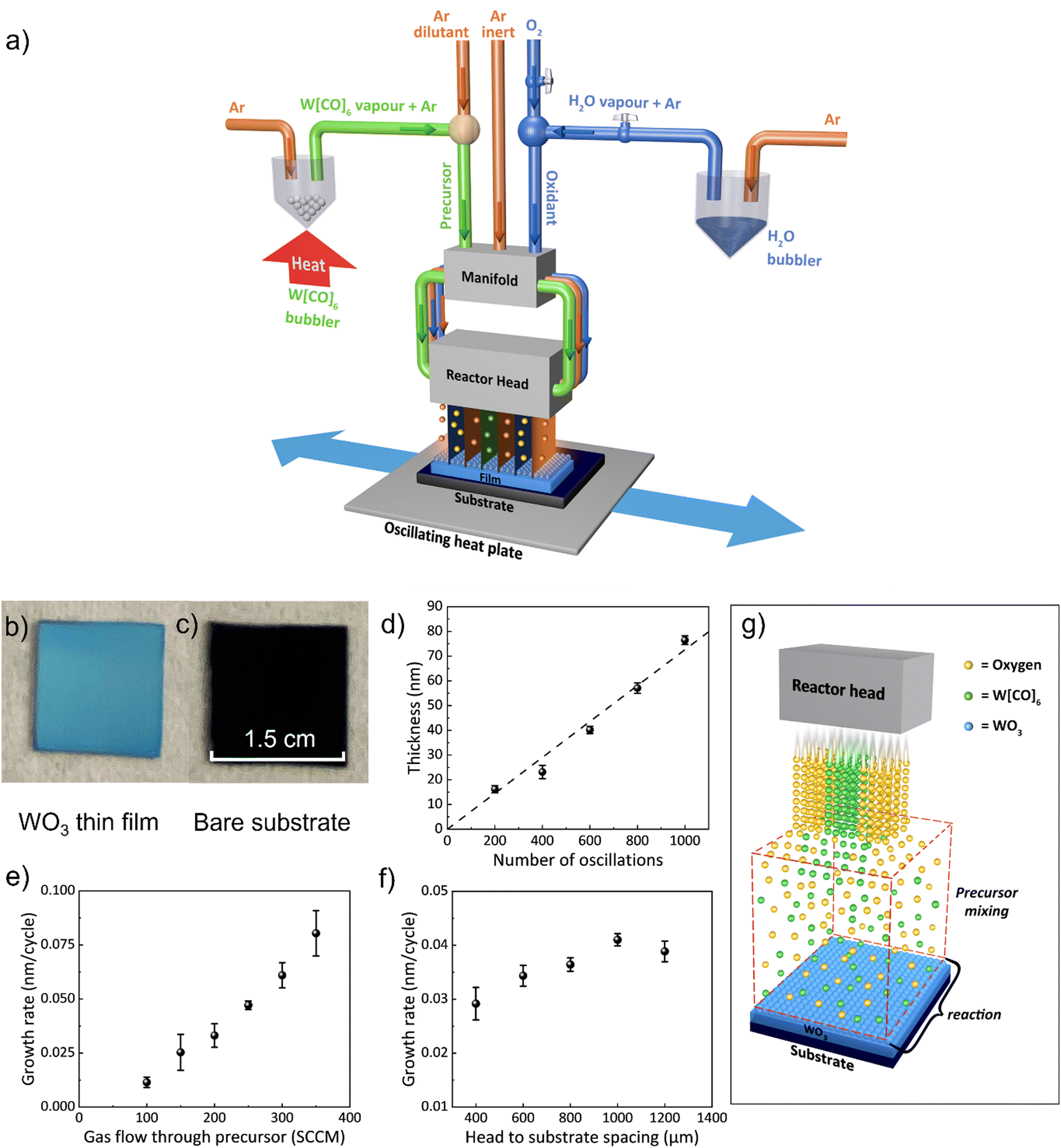 | ||
| Fig. 1 Basic properties of WO3 film growth using AP-SCVD. (a) Schematic of AP-SCVD system for the WO3 film deposition, (b) optical image of WO3 thin film grown on SiO2/Si substrate using O2 as the oxidant, (c) bare SiO2/Si substrate, (d) thickness of WO3 films on SiO2/Si substrate as a function of the number of substrate oscillations, (e) growth rate as a function of W[CO]6 bubbler flowrate at a head-to-substrate spacing of 800 μm, (f) film growth rate as a function of head to substrate spacing at an Ar through precursor flowrate of 200 sccm, (g) schematic diagram showing how gas mixing occurs under the reactor head to give a CVD growth mode. | ||
In terms of the oxidant gas, we found that both air and H2O resulted in non-uniform and slow deposition, whereas O2 gave the most uniform films and relatively high growth rates. We note that previously, for the growth of WO3 using the BTBMW precursor, O3 was found to be the optimum oxidant.41 Hence, all films reported in this work were grown using O2 as the oxidant which is advantageous over the toxic O3. A fixed oxygen flow rate of 100 sccm was used for all the films as this was found to be sufficient to oxidize the films. To explore film growth rates, a substrate oscillation speed of 50 mm s−1 was used.38
Fig. 1b shows an optical image of a WO3 film (30 nm) grown on a SiO2/Si substrate. Fig. 1c shows the bare substrate for comparison. It can be seen that conformal WO3 films were obtained over cm2 size and wafer size deposition can be feasible upon scaleup of the reactor head. Fig. 1d reveals the film thickness, measured by the profilometer, and verified by ellipsometry, over a range of oscillation cycles. The thickness was found to be dependent linearly (regression >0.99) on the number of oscillation cycles demonstrating precise film thickness control by this technique.39Fig. 1e shows the growth rate versus Ar gas flow rate through the tungsten precursor for a head-to-substrate spacing of 800 μm. There is an increasing growth rate with gas flow rate indicating CVD growth,38 also indicating the rate-limiting step in the growth is the tungsten precursor concentration in the gas above the substrate. From Fig. 1e, the average growth rate (i.e., thickness deposited per half oscillation) increases from 0.01 nm per cycle to 0.08 nm per cycle with an increased gas flow rate from 100 sccm to 350 sccm. Gas flow rates above 300 sccm resulted in non-uniform films, likely due to the non-uniform mixing of precursors across the substrate.
The spacing between the reactor head and the surface of the substrate is a unique deposition parameter for the AP-SCVD system. For many oxide films, the film performance is very similar for AP-SALD and AP-SCVD growth modes.37 However, for AP-SALD growth, there is the added complexity that head-to-substrate spacing needs to be as low as ∼20 μm37,38 to ensure the pressure gradient in each gas channel produces gas isolation to prevent precursor mixing in the gas phase.34,35,37 Since this head-to-substrate distance requires more complex alignment without distinct advantages, the use of AP-SCVD mode with a large head-to-substrate distance is preferred. Fig. 1f shows that a higher deposition rate occurs with increasing head-to-substrate spacing, again confirming CVD growth. Above a spacing of 1000 μm, growth saturation occurs, indicative of full gas mixing and reaction above the substrate. For a spacing of 200 μm and below, no deposition occurred, indicating that inadequate gas mixing and reaction occurred and that the substrate oscillation speed (50 mm s−1) was likely too high for any chemically reacted precursor to attach to the substrate surface. A substrate-to-head spacing of 1000 μm was used for further depositions as it produced uniform films at a high growth rate. The saturated deposition rate was found to be 0.04 nm per cycle which compares to ∼0.02 nm per cycle using conventional ALD with the same precursor.45–47 The CVD growth mode of the films in our AP-SCVD setup is illustrated in Fig. 1g.
2.2. Continuous tunability of film crystalline orientation
Fig. 2a shows the X-ray diffraction (XRD) patterns of the films that were obtained by tuning the oscillation speed and O![[thin space (1/6-em)]](https://www.rsc.org/images/entities/char_2009.gif) :W ratio, where O:W ratio is the ratio of oxygen flowrate and argon flowrate through precursor bubbler, with individual patterns numbered to correspond to the growth parameters of Fig. 2b. The deposited films are identified as monoclinic phase WO3 (Fig. S1, ESI†), which agrees well with films deposited by other researchers using conventional ALD and sputtering at temperatures close to 320 °C and is expected because monoclinic WO3 is the most stable phase from room temperature up to ∼500 °C.42,45,46,48 The O:W ratio is adjusted by only changing the Ar flowrate through the precursor bubbler whilst maintaining the oxygen flowrate. Therefore, the effect of the W:O ratio on the growth rate, as shown in Fig. S2 (ESI†) could also be calculated based on the data in Fig. 1e. The increase of W:O ratio leads to a linear increase in growth rate, indicating a CVD growth mode in the WO3 film growth. Fig. 2b shows a pseudo map of the proportion of the (0 0 2) XRD peak area with respect to the total peak area of the ‘(2 0 0) + (0 0 2)’ peaks for the different growth parameters. It can be observed from Fig. 2a and b that the WO3 film orientation can be continuously tuned, changing from (2 0 0) orientation to (0 0 2) depending on the substrate oscillation speed and O:W ratio. At low oscillation speed and low O:W ratio, the (2 0 0) peak dominates (condition 1 in Fig. 2b), whereas the (0 0 2) peak dominates for the opposite conditions (condition 9 in Fig. 2b). Furthermore, the growth rate for every condition in Fig. 2b was calculated as shown in Table S2 (ESI†). It could be seen a high growth rate of 1–5 nm min−1 could be realized under these conditions.
:W ratio, where O:W ratio is the ratio of oxygen flowrate and argon flowrate through precursor bubbler, with individual patterns numbered to correspond to the growth parameters of Fig. 2b. The deposited films are identified as monoclinic phase WO3 (Fig. S1, ESI†), which agrees well with films deposited by other researchers using conventional ALD and sputtering at temperatures close to 320 °C and is expected because monoclinic WO3 is the most stable phase from room temperature up to ∼500 °C.42,45,46,48 The O:W ratio is adjusted by only changing the Ar flowrate through the precursor bubbler whilst maintaining the oxygen flowrate. Therefore, the effect of the W:O ratio on the growth rate, as shown in Fig. S2 (ESI†) could also be calculated based on the data in Fig. 1e. The increase of W:O ratio leads to a linear increase in growth rate, indicating a CVD growth mode in the WO3 film growth. Fig. 2b shows a pseudo map of the proportion of the (0 0 2) XRD peak area with respect to the total peak area of the ‘(2 0 0) + (0 0 2)’ peaks for the different growth parameters. It can be observed from Fig. 2a and b that the WO3 film orientation can be continuously tuned, changing from (2 0 0) orientation to (0 0 2) depending on the substrate oscillation speed and O:W ratio. At low oscillation speed and low O:W ratio, the (2 0 0) peak dominates (condition 1 in Fig. 2b), whereas the (0 0 2) peak dominates for the opposite conditions (condition 9 in Fig. 2b). Furthermore, the growth rate for every condition in Fig. 2b was calculated as shown in Table S2 (ESI†). It could be seen a high growth rate of 1–5 nm min−1 could be realized under these conditions.
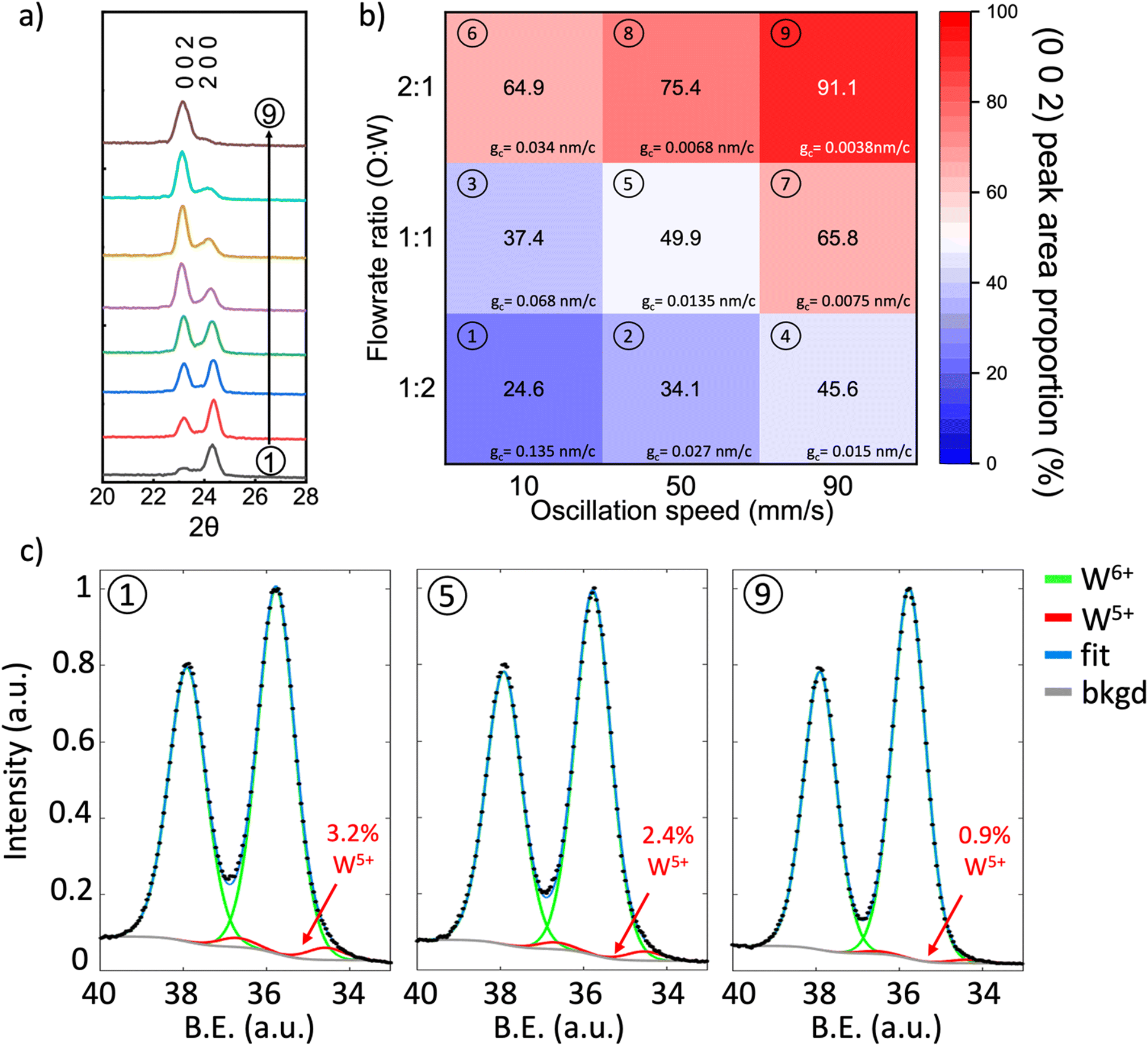 | ||
| Fig. 2 (a) XRD of as-deposited 30 nm WO3 films and (b) map of (0 0 2) peak area of WO3 films on SiO2/Si substrates grown on SiO2/Si substrates grown using various substrate oscillation speeds and O:W ratios, the corresponding growth rate per cycle, gc value (which will be analysed in details in further discussion) was also calculated for each condition. (c) W-4f XPS spectra of 30 nm (2 0 0) dominant (deposited in condition 1), (0 0 2) + (2 0 0) mixture (deposited in condition 5) and (0 0 2) dominant (deposited in condition 9) WO3 thin film (B.E. indicates binding energy). | ||
The oxidation states of different orientations were analyzed using high-resolution X-ray photoelectron spectroscopy (XPS). Fig. 2c shows XPS spectra for films grown at conditions 1 (left), 5 (middle), and 9 (right). All spectra show a doublet associated with the 7/2 and 5/2 spin–orbit splitting of W-4f around 35.8 eV (W-4f7/2) and 37.9 eV (W-4f5/2). We observe that while the peak splitting remains constant between films, there is a variation in spectrum shape, see XPS spectrum overlay in Fig. S3 (ESI†). This suggests the presence of multiple peak components within the W-4f spectra. As such, two sets of Gaussian (60%)-Lorentzian (40%) peaks were fit to W-4f spectra with a Shirley background. This fitting is comprised of a primary green peak pair associated with W6+ (WO3) around 35.8 eV (W-4f7/2) and 37.9 eV (W-4f5/2) and a smaller red peak pair from W5+ (WO2.5) at around 34.5 eV (W-4f7/2) and 36.6 eV (W-4f5/2). We note that no absolute energy calibration was used for the analysis of the XPS spectra, as peak area, not peak position, was used for W valency calculations. The presence of the W5+ peak indicates sub-stoichiometric tungsten oxide, i.e., WO3−x. Furthermore, the absence of C was further confirmed by time-of-flight elastic recoil detection analysis (ToF-ERDA) analysis was performed on a representative WO3 film grown under the oscillation speed of 50 mm s−1 and W:O ratio of 1:1 (Condition 5 as in Fig. 2b). No trace of C was found in the film, indicating that the precursor decomposition was complete and very clean WO3 films were made using the AP-SCVD technique.
From the W-4f spectrum in Fig. 2c for growth conditions 1, 5, and 9, corresponding to orientations (2 0 0), ‘(2 0 0) + (0 0 2)’, and (0 0 2), the W5+ peak makes up 3.2, 2.4, and 0.9 atomic percent of the film, respectively. The increasing W5+ is the result of a decrease in the average oxidation state (an increase in oxygen vacancies) in the ‘(2 0 0) + (0 0 2)’ type and (2 0 0) dominant films. This is consistent with previous observations for electrodeposited monoclinic WO3 of different orientations: a (2 0 0) dominant film showed the highest oxygen vacancy concentration and an (0 0 2) dominant film showed the lowest.26 Hence, the (0 0 2) dominant film (grown under condition 1 in Fig. 2b) is near stoichiometric in oxygen as there is only a minute W5+ fraction indicating x is very small in WO3−x. For the lowest calculated W5+ fraction (0.9 at%) of the film composition is calculated to be WO2.996, i.e., close to oxygen stoichiometric. Low oxygen vacancy content for (0 0 2) orientation is achieved with an oxygen to precursor ratio and high oscillation speed. To check the consistency of the growth conditions and XPS analysis, a second film was grown under condition 9 to produce another (0 0 2) dominant film. The W5+ was measured to make up 0.7 at% in this additional film, see Fig. S4 (ESI†) for the spectrum. This film deviates from the first film measurement for condition 9 by only 0.2 at%, showing that films grown under condition 9 are near stoichiometric in oxygen and that there is considerably less oxygen in the (2 0 0) dominant and ‘(2 0 0) + (0 0 2)’ films compared to the (0 0 2) dominant films.
Interestingly, all growth conditions produce films much closer to stoichiometric than those observed for other vapor growth methods of ALD, CVD, and AP-SCVD.41,49,50 For example, a previous atmospheric pressure CVD study using WCl6 as the precursor where the growth temperature is significantly higher than used here, i.e. 625 °C, WO3−x was grown and the oxygen stoichiometry was low, WO2.75 (the W-4f XPS spectrum is comprised of 15 at% W5+).49 This could be due to the incorporation of chlorine impurities upon deposition.51 Also, in an earlier study using AP-SCVD with BTBMW as the precursor, a film composition of WO2.3 was achieved.41 The significantly lower oxygen contents are potentially because the bulkier ligands in BTBMW are harder to remove and the nebulized droplets are less reactive compared to W[CO]6 vapor, thus leaving more reducing organic components in the film. Overall, the W[CO]6 precursor of this work yields near-oxygen stoichiometric WO3 thin films, particularly for higher O:W ratio and higher substrate oscillation speed which gives rise to a predominant (0 0 2) orientation.
Atomic force microscopy (AFM) images comparing the (2 0 0)-dominant film and (0 0 2)-dominant film (Fig. 3a and b, respectively) reveal different surface morphologies and grain sizes for the two different orientations. The (2 0 0) dominant film has large, rectangular grains which indicated grains growing parallel to the substrate. The grain size is 70.3 nm ± 37.7 nm and the roughness, Ra = 1.39 nm (Fig. 3a and Fig. S5a, ESI†). The (0 0 2)-dominant film, on the other hand, shows smaller clustered rectangular-shaped grains, consistent with the grains now pointing out-of-the plane of the film. The grain size is 34.9 nm ± 9.9 nm and roughness Ra = 1.50 nm (Fig. 3b and Fig. S5b, ESI†). Uniformity of the as-deposited WO3 film with different dominant orientations was confirmed by AFM characterization with a random selection of several spots, suggesting the high uniformity covering > cm2 area (Fig. S6, ESI†). The roughness values are relatively low and are comparable to WO3 films grown by ALD.47
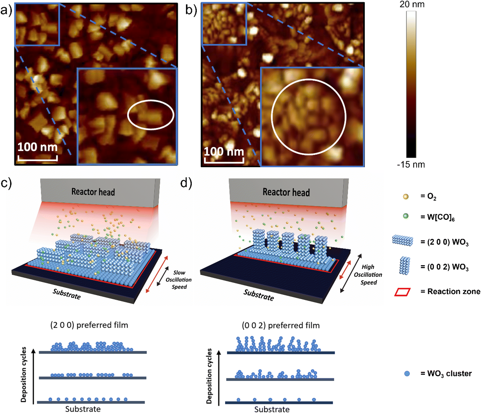 | ||
| Fig. 3 (a) AFM image of 30 nm (2 0 0) dominant WO3 film, (b) AFM image of 30 nm (0 0 2) dominant WO3 film, (c) schematic of WO3 film growth under low oscillation speed leading to higher nucleation density and greater lateral growth of islands producing the thermodynamically preferred (2 0 0) orientation, (d) schematic of WO3 film growth under high oscillation speed, leading to lower nucleation density and less lateral growth of islands, producing the kinetically preferred (0 0 2) orientation. | ||
The different orientations of the films, as determined from XRD, and the grain structures as determined by AFM can be understood based on earlier theoretical calculations, which show the (0 0 2) plane of monoclinic WO3 has the highest surface energy whereas the (2 0 0) plane has the lowest.52,53 High surface energy facets are normally associated with a high crystal growth rate and low thermodynamic stability.54 Therefore the (0 0 2) orientation would be preferred when the growth is kinetically limited, i.e. under high substrate oscillation speed and high O:W ratio (condition 9 in Fig. 2b). Under low substrate oscillation speeds, the precursor exposure time above the substrate per deposition cycle, is large. Under this condition, the reaction zone, a visual representation of precursor density exposure to the surface of the substrate per time, is also large, as shown schematically in Fig. 3c. This means the available reaction time during a deposition cycle is sufficient for a high nucleation density, and thus the thermodynamic (2 0 0) orientation is favored. Other experimental work for films grown by electrodeposition with post-annealing also finds that the (2 0 0) orientation is the thermodynamically favored product, formed when the nucleation density is high.26 In contrast, at higher oscillation speeds, the exposure time of the precursor to the substrate is decreased, and correspondingly the precursor density exposure to the surface also decreased, represented by a smaller reaction zone in Fig. 3d. Here, there is less time for reaction per deposition cycle, and low nucleation density can be expected. Hence, the kinetically preferred (0 0 2) orientation is obtained in the films.26
As shown in the previous section, the tungsten precursor rather than the oxidant gas was found to be the limiting reactant for the film growth. Therefore, when the O:W ratio is high, the concentration of tungsten precursor in the gas above the substrate is low, resulting in a reduced rate of reaction as well as nucleation density, favoring the (0 0 2) orientation. Conversely, at a low O:W ratio, the concentration of tungsten precursor is high with a fast rate of reaction and nucleation density, thus favoring the (2 0 0) orientation.
To better understand the growth mechanism of the as-deposited WO3 film in the AP-SCVD process, the total film thickness (t) can be defined by eqn (1),
| t = gc × n | (1) |
:W ratio. Therefore, we propose that gc is further defined as the combined effect related to the oscillation speed (v) and tungsten precursor input rate (rw) as defined by eqn (2),| gc ∝ 1/v × rw | (2) |
Here, the rw is determined by the flow rate of the tungsten precursor to the reactor head, which is controlled by the O:W ratio. A low gc can be realized when the oscillation speed and the O:W ratio are high, leading to (0 0 2) dominant film growth. In contrast, when the oscillation speed is low and the O:W ratio is small, a high gc can be achieved, and correspondingly a (2 0 0) dominant film will be expected to grow. The end film thickness can be controlled by n, where more deposition cycles will be needed if gc is low and fewer deposition cycles are needed at high gc.
In summary, by adjusting the substrate oscillation speed and the O:W ratio in the AP-SCVD process, we achieved in situ tuning of the preferred crystalline orientation of the as-deposited WO3 film on amorphous substrates, avoiding the use of post-deposition treatments or high-temperature growth, which are necessary for traditional thin-film deposition techniques. This rapid and low-thermal budget process achieved using AP-SCVD enables in-situ tuning of the preferred crystalline orientation of the WO3 film at constant temperature and pressure, which is highly desired for a wide range of applications, as noted above.
2.3. Photo-responsive behaviour of as-grown AP-SCVD WO3 thin films
To assess the performance of the WO3 films prepared by AP-SCVD, the performance of the WO3 films on various photo-responsive applications, i.e., PEC water splitting, UV photodetection, and photocatalytic degradation of MB was measured. For this, 30 nm as-deposited WO3 films of the three orientations grown in condition 1, condition 5, and condition 9 shown in Fig. 3b on SiO2/Si and FTO substrates were used.PEC studies were carried out at room temperature using a two-compartment configuration and three-electrode setup with WO3 deposited on FTO (area: 1 × 1 cm2) as the working electrode under 1 sun or 3 suns front-irradiation. Forward chopped CV scans (under 1 sun) from the PEC studies are shown in Fig. 4a (complete chopped, light, and dark scans are shown in Fig. S7, ESI†). It is observed that (0 0 2) dominant WO3 demonstrates the best performance toward PEC water oxidation with an onset potential of 0.66 ± 0.02 V vs. the reversible hydrogen electrode (RHE) and a maximum photocurrent density (J) of 0.12 mA cm−2 (at 1.23 V vs. RHE), followed by (0 0 2) + (2 0 0) oriented WO3 (onset potential: 0.68 ± 0.01 V vs. RHE; J = 0.09 mA cm−2 at 1.23 V vs. RHE) and (2 0 0) oriented WO3 (onset potential: 0.73 ± 0.02 V vs. RHE; J = 0.06 mA cm−2 at 1.23 V vs. RHE) at 1 sun irradiation. Therefore, WO3 of (0 0 2) oriented film generates two times higher current density compared to that of (2 0 0) oriented films as well as a lower onset potential. These higher current densities for the (0 0 2) orientation are consistent with earlier work on electrodeposited and annealed films.26 As expected, increasing the solar concentration to 3 suns resulted in the enhancement of J for the different WO3 photoanodes as shown in Fig. 4b. The onset potentials for (0 0 2), (0 0 2) + (2 0 0), and (2 0 0) oriented WO3 films at 3 suns irradiation were 0.64 ± 0.03 V vs. RHE (J = 0.25 mA cm−2 at 1.23 V vs. RHE), 0.67 ± 0.01 V vs. RHE (J = 0.15 mA cm−2 at 1.23 V vs. RHE) and 0.72 ± 0.01 V vs. RHE (J = 0.08 mA cm−2 at 1.23 V vs. RHE), respectively. The increasing onset potentials for the different orientations are also consistent with earlier work on electrodeposited and annealed films.26Table 1 summarizes the performance of the films of this work compared to other reported PEC devices based on planar WO3 thin films. Note: the valid comparison we have made is for films of thickness below 500 nm where surface roughening (leading to significantly larger effective surface area) would be less prominent. A higher photocurrent density can be seen in the (0 0 2) dominant WO3 film deposited by AP-SCVD. This value is higher or comparable to the films deposited under vacuum and with further post-deposition annealing treatment.
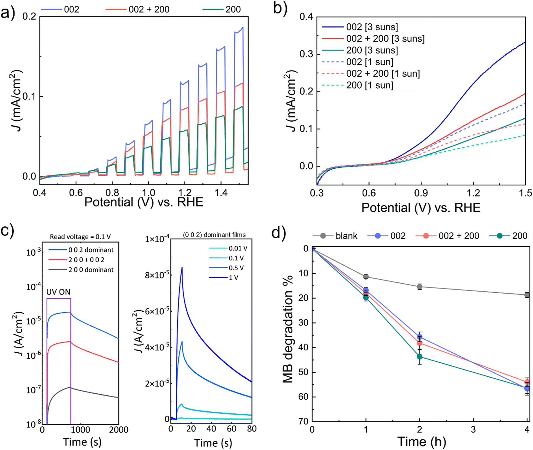 | ||
| Fig. 4 Photo-response of 30 nm WO3 thin films by AP-SCVD. (a) PEC water splitting: forward CV scans recorded under chopped simulated at 1 sun solar light irradiation for different oriented films on FTO. (b) PEC water splitting: forward CV scans under continuous light illumination (1 sun and 3 suns) for different oriented films on FTO. Conditions for PEC water splitting: 0.5 M aqueous NaCl electrolyte (pH ~6), inert atmosphere, room temperature, stirring. (c) UV photodetection properties of photocurrent density of different orientated films on Si substrate under UV illumination using a read voltage of 0.1 V for 600 s illumination time (left) and photocurrent density of (0 0 2) dominant film on Si under UV illumination at different read voltage for 5 s illumination time (right), (d) photocatalytic (PC) time-dependent methylene blue (MB) degradation of different orientated WO3 films under 1 sun irradiation. 'blank' refers to tests without any WO3 film under 1 sun illumination. Conditions: ~1 ppm aqueous MB concentration, room temperature, stirring. | ||
Next, the UV photodetector performance was measured on WO3 films on SiO2/Si substrates with the interdigital aluminium electrode (area 1 × 1 cm2) where the exposed film area is half of the electrode area. Fig. 4c (left) shows photocurrent density at a read voltage of 0.1 V for three devices made from WO3 films with three different types of dominant orientations. For a reading voltage of 0.1 V, we find that after 600 s of UV illumination the (0 0 2) dominant orientation film reaches saturation with a photocurrent density more than two orders of magnitude higher (2.59 × 10⁻⁵ A cm−2) than the (2 0 0) dominant orientation film (1.21 × 10⁻⁷ A cm−2), and one order of magnitude higher than the ‘(2 0 0) + (0 0 2)’ orientation film (2.56 × 10⁻⁶ A cm−2). Comparing the response times for the 3 films, we observe that the response time is shortest for the (0 0 2) dominant orientation film (262 s), and longest for the (2 0 0) dominant orientation film (492 s). The mixed ‘(2 0 0) + (0 0 2)’ orientation film produced intermediate performance (320 s). Hence, based on photocurrent density and response time, the (0 0 2) dominant orientation film has superior performance. This agrees with earlier work where it was shown the (0 0 2) orientation gives optimum UV photodetector performance.26
Fig. 4c (right) shows the photocurrent density of the (0 0 2) dominant orientation film in more depth, looking at different reading voltages ranging from 0.001 V to 1 V with 5 s UV illumination time. We find that there is a significant photocurrent density increase with reading voltage, as would be expected with a larger internal gain. For a read voltage of 1 V, a maximum responsivity of ∼10−3 A W−1 was measured with a rise time of 3.63 s. Hence, for the (0 0 2) orientation, more photoelectrons and holes are generated in a shorter period at a higher internal gain. Table 2 summarizes the responsivity and rise time for our (0 0 2) oriented films made by AP-SCVD to have faster rise times and higher responsivity values than other reported WO3 devices using thin film deposition processes which require either vacuum conditions and/or higher deposition temperatures, and/or post-annealing. Only one low-temperature grown film of 225 nm thickness, grown using DC sputtering has a better performance.53 Here, the responsivity values are higher although samples were grown under vacuum, were biased at 3 V instead of 1 V, and incident light wavelength of 385 nm instead of 410 nm, as used in our work.
| Vacuum | Deposition temp. (°C) | Post-annealing | λ (nm) | Bias (V) | Responsivity (A W−1) | Rise time (s) | Year & ref. |
|---|---|---|---|---|---|---|---|
| No | RT | 600 °C | 410 | N/A | 2.68 × 10⁻² | 400 | 201457 |
| Yes | N/A | No | 370 | N/A | 1.70 × 10⁻⁷ | 48 | 201558 |
| Yes | 170 | 380 °C | 365 | <1 | 1.75 × 10⁻⁵ | 10.2 | 201959 |
| Yes | 200 | No | 385 | 3 | 1.66 × 10⁻¹ | ∼1 | 202153 |
| No | 320 | No | 400 | 1 | 1.00 × 10⁻³ | 3.6 | This work |
Finally, photocatalytic (PC) degradation of methylene blue (MB) experiments was explored for the AP-SCVD films. WO3 films of (0 0 2), (0 0 2) + (2 0 0), and (2 0 0) orientation (deposited on 1 × 1 cm2 area FTO as before for consistency, but can also be deposited on other transparent, non-conducting substrates for PC degradation studies) were immersed in aqueous MB. In this case, all the WO3 films were active towards the solar-driven degradation of MB with time, with similar degradation efficiencies (∼50–60% after 4 h); Fig. 4d and Fig. S8(a–c) (ESI†) show that the (2 0 0) oriented WO3 film exhibited marginally better activity during the initial stages. Control exclusion experiments in the absence of light did not lead to appreciable MB degradation, whereas those in the absence of WO3 showed slight photo-induced MB degradation (~15% after 2 h) with time (Fig. S8d and e, ESI†). The improvement of PEC, UV detection, and photocatalytic performance by tuning the film orientation is in good agreement with previous studies of films made by electrodeposition with post-deposition annealing.26Table 3 summarizes the performance for PC degradation of MB of the films of this study compared to other planar WO3 thin films in the literature. Note- as for the PEC data, the valid comparison is for films of thickness below 500 nm where surface roughening (leading to significantly larger surface area) would be less prominent. Table 3 shows that the (2 0 0) dominant WO3 film deposited by AP-SCVD shows a faster degradation rate by up to around a factor of 2 relative to planar films deposited by vacuum methods which also require post-annealing.
To confirm the reason why the (0 0 2) orientation films give optimum performance for PEC and UV detection and better initial PC degradation, ellipsometry analysis was conducted to determine the bandgaps of the different WO3 films. Fig. S9 (ESI†) shows that (0 0 2) oriented film has a lower bandgap than the ‘(2 0 0) + (0 0 2)’ oriented and (2 0 0) oriented films. Linking this back to the XPS data of Fig. 3c, which showed that a higher (0 0 2) fraction resulted in higher oxygen content in the films, we can determine that the bandgap decreases with higher oxygen content. This is consistent with previous work and is explained by the electronic band structure being influenced by the crystallographic locations of oxygen vacancies.26 The lower bandgap and higher oxygen content of the (0 0 2) film are favorable for optical absorption as it enhances the photogeneration of charge carriers and reduces the recombination of photogenerated electrons and holes (less deep oxygen vacancy defects to act as recombination sites). This explains the superior photocurrent density and faster response times for PEC (Fig. 4a) and the superior photodetection (Fig. 4c) were observed for our (0 0 2) oriented films.26–28 The influence of film orientation was more pronounced for PEC and photodetection than for photocatalytic degradation (Fig. 4d). This is because for photocatalytic degradation, oxygen vacancies are important to act as adsorption sites for methylene blue, but the charge carrier dynamics are not important since charge carrier transport does not occur. Thus, the more oxygen-deficient (2 0 0) oriented films give an enhanced degradation rate.55 On the other hand, the higher bandgap in the (2 0 0) film would lead to lower light absorption, explaining why there is a diminishing difference in the performance of the differently oriented devices for longer degradation times.26 This could be the possible reason why we observed a better initial PC performance for the film with (2 0 0) orientation but the long-term behavior is less significant for different orientations of the WO3 films.
Overall, low-temperature-grown AP-SCVD WO3 films show strong performance in three photo-responsive applications compared to films grown either under vacuum and/or at higher temperature and/or with higher temperature post-annealing. A key question is why this is the case. When it comes to depositing oxide thin films by ALD and CVD, the reactivity of the precursor is key to achieving low-temperature growth and high-quality films.56 It is well known that heat is released (exothermic reaction63,64) during each deposition cycle for ALD growth adding additional energy to the system and increasing the local temperature. This heat will add to the heat of the substrate and improve the film crystallinity.
The decomposition of W[CO]6 (combustion) on the substrate surface follows the exothermic reaction:
| W(CO)6 + 9/2O2 → WO3 + 6CO2 | (3) |
3. Conclusions
In this paper, we fabricated highly crystalline and near-oxygen stoichiometric WO3−x films via a scalable and simple, high-throughput atmospheric pressure spatial chemical vapor deposition (AP-SCVD) method. Using the method, films are grown in an open-atmosphere environment at a CMOS-compatible temperature of 320 °C using relatively benign precursors and gases. More importantly, using the very simple parameter adjustments of changing substrate oscillation speed (a parameter unique to AP-SCVD) under the precursor delivery head, and the flowrate ratio of oxygen to precursor, the preferred film orientation was tuned continuously from (2 0 0) dominant to (0 0 2) dominant. The preferred film orientations were applied in PEC water splitting, UV photodetection, and photocatalytic pollutant degradation, where it was found that the (0 0 2) dominant orientation device exhibited a much superior photodetection and water splitting performance compared to the other orientation films while (2 0 0) oriented device had a faster initial photocatalytic degradation rate but the long-term degradation was less significant for different orientations. The film performances were in most cases equivalent to or superior to previously reported films made under vacuum using higher temperature growth and/or higher temperature post-annealing. Overall, AP-SCVD has strong potential as an industrially scalable thin-film deposition technique for producing high-quality oxide films at CMOS-compatible temperatures, with in-situ tuning of film properties, as demonstrated here for WO3.4. Experimental method
4.1. Film deposition
WO3 films were deposited on SiO2/Si substrates using a custom-built AP-SCVD system located in a fume cupboard. In the system, the precursor gas, Ar (inert), and oxidant (either O2, or H2O bubbled with Ar) gas channels all feed through a manifold which then passes the gases to the reactor head where they exit in alternating positions (see Fig. 1a). The dimensions of the reactor header here are 70 mm by 30 mm by 40 mm. The oxidant gas was controlled by using the valves on the tubing before entering the manifold as shown in Fig. 1a. When H2O was used, a fixed 100 sccm of Ar gas was passed through the H2O bubbler, while when O2 was used, a fixed 100 sccm of O2 gas was fed directly into the manifold. Air was also used as an oxidant. In that case, no gas was fed into the oxidant channel. The tungsten precursor W[CO]6 was placed in a bubbler in its solid form and heated to 70 °C using an oil bath to obtain adequate vapor pressure.73 The precursor gas line was further heated by wrapping a heating tape to ensure the precursor did not condense during the experiments. Ar gas was passed through the W[CO]6 bubbler and the metal precursor was diluted with an additional 100 sccm of Ar from an Ar dilutant channel before entering the reactor head. The Ar gas flow rate was maintained at 500 sccm for all depositions. These flow rates were used previously in our system to give high-quality ZnO films.38Below the reactor head is an oscillating temperature-controlled hotplate, where the substrate is placed. A water circulation system is connected to the reactor head to keep the temperature down due to the proximity of the head to the hotplate. During every deposition, the substrate temperature was maintained at 320 °C. This temperature was the lowest possible for achieving uniform coverage films (no deposition took place below 300 °C). All samples were grown on silicon substrates with a 90 nm oxide layer.
For phase identification and materials characterization, a 200 nm film was deposited with a gas flow rate through the precursor of 200 sccm, a substrate oscillation speed of 50 mm s−1 and a head-to-substrate spacing of 1000 μm. These conditions provided sufficient film thickness and hence measurement signal for each characterization method. For orientation tuning and photodetector device fabrication, 30 nm films were deposited at a fixed head-to-substrate spacing of 1000 μm while adjusting the gas flow rate through the precursor from 100 sccm to 350 sccm and substrate oscillation speed from 10 mm s−1 to 90 mm s−1.
4.2. Film characterization
The film thickness was determined using a surface profiling technique via a Dektak 6M stylus profiler. The film thickness was further verified using a J.A. Woolam Co., Inc. EC-400 ellipsometer using a 75 W Xe light source, where the change in the polarization of light upon the reflection of the substrate through the film was correlated for the thickness and refractive index. X-ray diffraction patterns were obtained using a Bruker D8 Advance X-ray diffractometer with a position-sensitive detector and Bragg Brentano para-focusing geometry. A Gaussian model was used to fit the relative peak area of different film orientations shown on XRD graphs. Raman spectroscopy was conducted using a Renishaw inVia Raman microscope using a 514 nm incident laser. X-ray photoelectron spectroscopy (XPS) was undertaken using an Al kα1 X-ray source (hγ = 1486.6 eV) and a SPECS PHOIBOS 150 electron energy analyzer. Ag paste was placed on the film edges to reduce charging and the O 1s peak was used for a relative binding energy calibration between films. The surface topology of the films was characterized using a Bruker Dimension atomic force microscope (AFM) and the images were analyzed with nanoscope analysis. The bandgaps for the WO3 films were estimated utilizing a Film Sense FS-XY150 ellipsometer. A Tauc-Lorentz model was used to fit the structure containing three separate layers to describe the samples: a Si substrate, a SiO2 layer, and a WO3 layer (the Tauc–Lorentz layer) on top. From fitting data to the model, information such as film thickness and bandgap values for the WO3 films was obtained. The bandgaps for the WO3 films were recorded when the estimated thickness for the WO3 and SiO2 layers was very close to those determined by profilometry or to the values provided by the wafer supplier.4.3. Device fabrication and characterization
| E(RHE) = E(Ag/AgCl) + 0.197 V + 0.059 × pH | (4) |
 | (5) |
Data availability
All data needed to evaluate the conclusions in this paper are present in the paper and/or in the ESI.† Original raw data that support the findings of this study are openly available in the Apollo repository at www.repository.cam.ac.uk/ with the DOI: 10.17863/CAM.106719.Author contributions
The manuscript was written through the contributions of all authors. All authors have given approval to the final version of the manuscript.Conflicts of interest
The authors declare no competing financial interests.Acknowledgements
Zhuotong Sun, Ming Xiao, and Judith L. MacManus-Driscoll thank the Royal Academy of Engineering grant, CIET1819_24, for funding. Subhajit Bhattacharjee thanks the Cambridge Trust (HRH The Prince of Wales Commonwealth Scholarship) for funding. Judith L. MacManus-Driscoll and Rob Jagt also thank Bill Welland for funding, as well as EPSRC grant EP/N509620/1 for funding a PhD studentship. Megan Hill thanks the Herchel Smith Foundation for a research fellowship. Kevin Musselman and Louis-Vincent Delumeau thank the Canada Foundation for Innovation Exceptional Opportunities Fund, Project 41017, for funding. The authors also thank Babak Bhakit for facilitating the ToF-ERDA analysis of the film, Yang Li on Raman characterization, and Qingshen Jing and Nives Strkalj for fruitful discussion on the figures.References
- K. Miyake, H. Kaneko, M. Sano and N. Suedomi, J. Appl. Phys., 1984, 55, 2747–2753 CrossRef CAS.
- Y. Zhao, S. Balasubramanyam, R. Sinha, R. Lavrijsen, M. A. Verheijen, A. A. Bol and A. Bieberle-Hütter, ACS Appl. Energy Mater., 2018, 1, 5887–5895 CrossRef CAS.
- J. Z. Ou, R. A. Rani, S. Balendhran, A. S. Zoolfakar, M. R. Field, S. Zhuiykov, A. P. O’Mullane and K. Kalantar-Zadeh, Electrochem. Commun., 2013, 27, 128–132 CrossRef CAS.
- S. Masi, R. Mastria, R. Scarfiello, S. Carallo, C. Nobile, S. Gambino, T. Sibillano, C. Giannini, S. Colella, A. Listorti, P. D. Cozzoli and A. Rizzo, Phys. Chem. Chem. Phys., 2018, 20, 11396–11404 RSC.
- Z. Hai, Z. Wei, C. Xue, H. Xu and F. Verpoort, J. Mater. Chem. C, 2019, 7, 12968–12990 RSC.
- V. R. Buch, A. K. Chawla and S. K. Rawal, Mater. Today Proc., 2016, 3, 1429–1437 CrossRef.
- C. Dong, R. Zhao, L. Yao, Y. Ran, X. Zhang and Y. Wang, J. Alloys Compd., 2020, 820, 153194 CrossRef CAS.
- Z. Hai, M. Karbalaei Akbari, Z. Wei, C. Xue, H. Xu, J. Hu and S. Zhuiykov, Electrochim. Acta, 2017, 246, 625–633 CrossRef CAS.
- K. Qian, G. Cai, V. C. Nguyen, T. Chen and P. S. Lee, ACS Appl. Mater. Interfaces, 2016, 8, 27885–27891 CrossRef CAS.
- J. T. Yang, C. Ge, J. Y. Du, H. Y. Huang, M. He, C. Wang, H. bin Lu, G. Z. Yang and K. J. Jin, Adv. Mater., 2018, 30, 1–10 Search PubMed.
- H. H. Lu, J. Alloys Compd., 2008, 465, 429–435 CrossRef CAS.
- V. Madhavi, P. Kondaiah, O. M. Hussain and S. Uthanna, ISRN Opt., 2012, 1–8 Search PubMed.
- S. Won, S. Y. Lee, J. Park and H. Seo, Sci. Rep., 2017, 7, 1–8 CrossRef CAS PubMed.
- S. Li, Z. Yao, J. Zhou, R. Zhang and H. Shen, Mater. Lett., 2017, 195, 213–216 CrossRef CAS.
- Y. T. Li, S. B. Long, H. B. Lü, Q. Liu, Q. Wang, Y. Wang, S. Zhang, W. T. Lian, S. Liu and M. Liu, Chin. Phys. B, 2011, 20, 017305 CrossRef.
- X. Sun, H. Cao, Z. Liu and J. Li, Appl. Surf. Sci., 2009, 255, 8629–8633 CrossRef CAS.
- M. Regragui, M. Addou, B. el Idrissi, J. C. Bernède, A. Outzourhit and E. Ec-chamikh, Mater. Chem. Phys., 2001, 70, 84–89 CrossRef CAS.
- P. O. Oviroh, R. Akbarzadeh, D. Pan, R. A. M. Coetzee and T. C. Jen, Sci. Technol. Adv. Mater., 2019, 20, 465–496 CrossRef PubMed.
- S. Zhuiykov, L. Hyde, Z. Hai, M. K. Akbari, E. Kats, C. Detavernier, C. Xue and H. Xu, Appl. Mater. Today, 2017, 6, 44–53 CrossRef.
- W. A. Bryant, J. Mater. Sci., 1977, 12, 1285–1306 CrossRef CAS.
- A. C. Jones and M. L. Hitchman, Overview of Chemical Vapour Deposition, in book “Chemical Vapour Deposition: Precursors, Processes and Applications” 2009, 1, 1–36.
- D. Davazoglou, A. Donnadieu and O. Bohnke, Sol. Energy Mater., 1987, 16, 55–65 CrossRef CAS.
- D. Vernardou, K. Psifis, D. Louloudakis, G. Papadimitropoulos, D. Davazoglou, N. Katsarakis and E. Koudoumas, J. Electrochem. Soc., 2015, 162, H579–H582 CrossRef CAS.
- K. L. Choy, Prog. Mater. Sci., 2003, 48, 57–170 CrossRef CAS.
- J. Y. Zheng, G. Song, C. W. Kim and Y. S. Kang, Nanoscale, 2013, 5, 5279–5282 RSC.
- W. L. Kwong, P. Koshy, J. N. Hart, W. Xu and C. C. Sorrell, Sustainable Energy Fuels, 2018, 2, 2224–2236 RSC.
- J. Y. Zheng, G. Song, J. Hong, T. K. Van, A. U. Pawar, D. Y. Kim, C. W. Kim, Z. Haider and Y. S. Kang, Cryst. Growth Des., 2014, 14, 6057–6066 CrossRef CAS.
- J. Zhang, P. Zhang, T. Wang and J. Gong, Nano Energy, 2015, 11, 189–195 CrossRef CAS.
- N. Zhang, C. Chen, Z. Mei, X. Liu, X. Qu, Y. Li, S. Li, W. Qi, Y. Zhang, J. Ye, V. A. L. Roy and R. Ma, ACS Appl. Mater. Interfaces, 2016, 8, 10367–10374 CrossRef CAS.
- P. Tägtström and U. Jansson, Thin Solid Films, 1999, 352, 107–113 CrossRef.
- A. Ito and Y. Morishita, Mater. Lett., 2019, 258, 126817 CrossRef.
- V. Jadkar, A. Pawbake, R. Waykar, A. Jadhavar, A. Date, D. Late, H. Pathan, S. Gosavi and S. Jadkar, Phys. Status Solidi A, 2017, 214, 1600717 CrossRef.
- Y. Guo, X. Quan, N. Lu, H. Zhao and S. Chen, Environ. Sci. Technol., 2007, 41, 4422–4427 CrossRef CAS PubMed.
- D. Muñoz-Rojas and J. Macmanus-Driscoll, Mater. Horiz., 2014, 1, 314–320 RSC.
- D. Muñoz-Rojas, V. H. Nguyen, C. Masse de la Huerta, S. Aghazadehchors, C. Jiménez and D. Bellet, C. R. Phys., 2017, 18, 391–400 CrossRef.
- K. P. Musselman, D. Muñoz-Rojas, R. L. Z. Hoye, H. Sun, S. L. Sahonta, E. Croft, M. L. Böhm, C. Ducati and J. L. MacManus-Driscoll, Nanoscale Horiz., 2017, 2, 110–117 RSC.
- R. L. Z. Hoye, D. Muñoz-Rojas, S. F. Nelson, A. Illiberi, P. Poodt, F. Roozeboom and J. L. Macmanus-Driscoll, APL Mater., 2015, 3, 040701 CrossRef.
- R. L. Z. Hoye, D. Muñoz-Rojas, K. P. Musselman, Y. Vaynzof and J. L. MacManus-Driscoll, ACS Appl. Mater. Interfaces, 2015, 7, 10684–10694 CrossRef CAS PubMed.
- R. A. Jagt, T. N. Huq, S. A. Hill, M. Thway, T. Liu, M. Napari, B. Roose, K. Gałkowski, W. Li, S. F. Lin, S. D. Stranks, J. L. MacManus-Driscoll and R. L. Z. Hoye, ACS Energy Lett., 2020, 5, 2456–2465 CrossRef CAS.
- R. D. Raninga, R. A. Jagt, S. Béchu, T. N. Huq, W. Li, M. Nikolka, Y. H. Lin, M. Sun, Z. Li, W. Li, M. Bouttemy, M. Frégnaux, H. J. Snaith, P. Schulz, J. L. MacManus-Driscoll and R. L. Z. Hoye, Nano Energy, 2020, 75, 104946 CrossRef CAS.
- T. W.-K. Yeow, K. Mistry, A. Shahin, M. Yavuz and K. P. Musselman, J. Vac. Sci. Technol., 2020, 38, 052411 CrossRef CAS.
- C. Charles, N. Martin, M. Devel, J. Ollitrault and A. Billard, Thin Solid Films, 2013, 534, 275–281 CrossRef CAS.
- K. P. Musselman, C. F. Uzoma and M. S. Miller, Chem. Mater., 2016, 28, 8443–8452 CrossRef CAS.
- D. K. Nandi and S. K. Sarkar, Energy Procedia, 2014, 54, 782–788 CrossRef CAS.
- J. Malm, T. Sajavaara and M. Karppinen, Chem. Vap. Deposition, 2012, 18, 245–248 CrossRef CAS.
- E. Salje and K. Viswanathan, Acta Crystallogr., Sect. A: Found. Crystallogr., 1975, 31, 356–359 CrossRef.
- C. S. Blackman and I. P. Parkin, Chem. Mater., 2005, 17, 1583–1590 CrossRef CAS.
- T. Zhang, C. Y. Lee, B. Gong and B. Hoex, AIP Conf. Proc., 1999, 2018, 040027 Search PubMed.
- K. Bergum, A. Magrasó, H. Fjellvåg and O. Nilsen, J. Mater. Chem. A, 2014, 2, 18463–18471 RSC.
- Y. P. Xie, G. Liu, L. Yin and H. M. Cheng, J. Mater. Chem., 2012, 22, 6746–6751 RSC.
- D. Zhang, S. Wang, J. Zhu, H. Li and Y. Lu, Appl. Catal., B, 2012, 123–124, 398–404 CrossRef CAS.
- H. Fredriksson and U. Akerlind, Solidification and Crystallization Processing in Metals and Alloys, Wiley, 2012 Search PubMed.
- P. V. K. Yadav, B. Ajitha, Y. A. Kumar Reddy and V. R. Minnam Reddy, ACS Appl. Electron Mater., 2021, 3, 2056–2066 CrossRef CAS.
- Y. Lv, Y. Liu, Y. Zhu and Y. Zhu, J. Mater. Chem. A, 2014, 2, 1174–1182 RSC.
- S. S. Kalanur, Catalysts, 2019, 9, 456 CrossRef CAS.
- D. Chua, S. B. Kim, K. Li and R. Gordon, ACS Appl. Energy Mater., 2019, 2, 7750–7756 CrossRef CAS.
- B. R. Huang, S. C. Hung, C. Y. Lin and Y. J. Chen, J. Mater. Sci.: Mater. Electron., 2014, 25, 408–413 CrossRef CAS.
- Y. M. Juan, S. J. Chang, H. T. Hsueh, T. C. Chen, S. W. Huang, Y. H. Lee, T. J. Hsueh and C. L. Wu, Sens. Actuators, B, 2015, 219, 43–49 CrossRef CAS.
- Z. Y. Hai, M. K. Akbari, Z. H. Wei, J. Zuallaert, W. D. Neve, C. Y. Xue, H. Y. Xu, F. Verpoort and S. Zhuiykov, ACS Appl. Mater. Interfaces, 2019, 11(31), 27997–28004 CrossRef CAS PubMed.
- H. W. Choi, E. J. Kim and S. H. Hahn, Chem. Eng. J., 2010, 161(1–2), 285–288 CrossRef CAS.
- A. Arfaoui, S. Touihri, A. Mhamdi, A. Labidi and T. Manoubi, Appl. Surf. Sci., 2015, 357, 1089–1096 CrossRef CAS.
- H. Li, Z. X. Mu, S. G. Liu and J. L. Zhang, Mat. Sci. Semicon. Proc., 2019, 99, 99–105 CrossRef CAS.
- O. Nilsen and H. Fjellvåg, J. Therm. Anal. Calorim., 2011, 105, 33–37 CrossRef CAS.
- A. R. Bielinski, E. P. Kamphaus, L. Cheng and A. B. F. Martinson, J. Am. Chem. Soc., 2022, 144, 15203–15210 CrossRef CAS PubMed.
- D. S. Barnes, G. Pilcher, D. A. Pittam, H. A. Skinner and D. Todd, J. Less-Common Met., 1974, 38, 53–58 CrossRef CAS.
- T. H. Wang, A. M. Navarrete-López, S. Li, D. A. Dixon and J. L. Gole, J. Phys. Chem. A, 2010, 114, 7561–7570 CrossRef CAS PubMed.
- D. Saha, R. S. Ajimsha, K. Rajiv, C. Mukherjee, M. Gupta, P. Misra and L. M. Kukreja, Appl. Surf. Sci., 2014, 315, 116–123 CrossRef CAS.
- L. Dunlop, A. Kursumovic and J. L. MacManus-Driscoll, Appl. Phys. Lett., 2008, 93, 98–101 CrossRef.
- J. Iqbal, A. Jilani, P. M. Ziaul Hassan, S. Rafique, R. Jafer and A. A. Alghamdi, J. King. Saud. Univ. Sci., 2016, 28, 347–354 CrossRef.
- T. Tan, Z. Liu, H. Lu, W. Liu and H. Tian, Opt. Mater., 2010, 32, 432–435 CrossRef CAS.
- T. Nakajima, T. Kitamura and T. Tsuchiya, Appl. Catal., B, 2011, 108–109, 47–53 CrossRef CAS.
- A. S. Nair, K. C. S. J. E. Abraham, P. George, C. Joseph, P. R. Biju and N. V. Unnikrishnan, Vacuum, 2022, 202, 111143 CrossRef CAS.
- M. A. Mamun, K. Zhang, H. Baumgart and A. A. Elmustafa, ECS J. Solid State Sci. Technol., 2015, 4, P398–P401 CrossRef CAS.
- S. Bhattacharjee, V. Andrei, C. Pornrungroj, M. Rahaman, C. M. Pichler and E. Reisner, Adv. Funct. Mater., 2022, 32, 2109313 CrossRef CAS.
- S. Das, S. Bhattacharjee, S. Mondal, S. Dutta, N. Bothra, S. K. Pati and S. Bhattacharyya, ACS Sustainable Chem. Eng., 2021, 9, 14868–14880 CrossRef CAS.
Footnotes |
| † Electronic supplementary information (ESI) available. See DOI: https://doi.org/10.1039/d3tc02257a |
| ‡ Present address: School of Microelectronics Science and Technology, Sun Yat-sen University, Zhuhai, 519082, Guangdong Province, China. |
| This journal is © The Royal Society of Chemistry 2024 |