
 Open Access Article
 This Open Access Article is licensed under a
 Creative Commons Attribution 3.0 Unported Licence
Phase-engineering compact and flexible CsPbBr3 microcrystal films for robust X-ray detection†
Lotte
Clinckemalie
 a,
Bapi
Pradhan
*a,
Roel Vanden
Brande
a,
Heng
Zhang
b,
Jonathan
Vandenwijngaerden
a,
Rafikul Ali
Saha
c,
Giacomo
Romolini
a,
Li
Sun
a,
Dirk
Vandenbroucke
d,
Mischa
Bonn
b,
Hai I.
Wang
b and
Elke
Debroye
*a
a,
Bapi
Pradhan
*a,
Roel Vanden
Brande
a,
Heng
Zhang
b,
Jonathan
Vandenwijngaerden
a,
Rafikul Ali
Saha
c,
Giacomo
Romolini
a,
Li
Sun
a,
Dirk
Vandenbroucke
d,
Mischa
Bonn
b,
Hai I.
Wang
b and
Elke
Debroye
*a
aDepartment of Chemistry, KU Leuven, Celestijnenlaan 200F, 3001, Leuven, Belgium. E-mail: elke.debroye@kuleuven.be; bapi.pradhan@kuleuven.be
bMax Planck Institute for Polymer Research, 55128 Mainz, Germany
ccMACS, Department of Microbial and Molecular Systems, KU Leuven, Celestijnenlaan 200F, 3001 Leuven, Belgium
dAgfa-Gevaert, Septestraat 27, B-2640 Mortsel, Belgium
First published on 11th December 2023
Abstract
All-inorganic CsPbBr3 perovskites have gained significant attention due to their potential in direct X-ray detection. The fabrication of stable, pinhole-free thick films remains challenging, hindering their integration in durable, large-area high-resolution devices. In this study, we propose a facile strategy using a non-conductive polymer to create a flexible, compact thick film under ambient conditions. Furthermore, we investigate the effect of introducing the 2D CsPb2Br5 phase into CsPbBr3 perovskite crystals on their photophysical properties and charge transport. Upon X-ray exposure, the devices consisting of the dual phase exhibit improved stability and more effective operation at higher voltages. Rietveld refinement shows that, due to the presence of the second phase, local distortions and Pb-vacancies are introduced within the CsPbBr3 lattice. This in turn presumably increases the ion migration energy barrier, resulting in a very low dark current and hence, enhanced stability. This feature might benefit local charge extraction and, ultimately, the X-ray image resolution. These findings also suggest that introducing a second phase in the perovskite structure can be advantageous for efficient photon-to-charge carrier conversion, as applied in medical imaging.
Introduction
Metal halide perovskite semiconductor materials have attracted significant attention owing to their exceptional optoelectronic properties, such as strong light absorption,1 high carrier mobility,2 and long electron–hole diffusion lengths.3 Their low-cost fabrication, in combination with the ability to tune their optical and electronic properties through their compositional and morphological flexibility, have made diverse perovskite compounds the focus of intense study for different applications such as solar cells,4 light emission applications (LEDs)5,6 and photo- and X-ray detection.7,8 X-ray detection is a crucial technology in many areas, such as medical imaging, industry and security screening, and material analysis.9,10 Over the years, the soft X-ray industry is transitioning from indirect detectors, in which a scintillator material is coupled to a photodetector, to more sensitive direct-conversion X-ray detectors.11 Most commercially available detectors are based on a semiconductor material, such as cadmium (zinc) telluride, or amorphous selenium (a-Se), which is currently used in mammography. However, the high cost and complex fabrication processes, or operational instability of these materials in combination with the low X-ray attenuation of a-Se constitute a significant bottleneck for their commercial usage.12–16All-inorganic CsPbBr3 perovskite has demonstrated significant potential in this field due to its large X-ray attenuation coefficient arising from the high average atomic number combined with intrinsic defect tolerance and good charge collection efficiency.15,17–20 It exhibits an intermediate bandgap energy, which is advantageous compared to the high bandgap of CsPbCl3. Additionally, it has an improved room temperature stability compared to CsPbI3, which only exhibits its photoactive perovskite phase above 350 °C.21–23 Despite its many advantages, several challenges need to be addressed before it can be fully commercialized for X-ray detection applications. One of the main obstacles is the stability of the material, as it is sensitive to moisture and heat, and prone to degradation, promoting the formation of detrimental defects and sacrificing the device performance.24–27 Furthermore, high-quality, phase-pure CsPbBr3 crystals are often synthesized via complex, prolonged and high-temperature synthesis methods, making it difficult to produce them on a large scale.28–30 Finally, fabricating high-quality, thick perovskite films remains a great challenge, primarily due to the presence of numerous pinholes that often occur as a result of solvent evaporation in the typical solution-based processes.19
In this paper, we developed a facile, room-temperature microcrystal synthesis strategy without the need of ligands and with precise control over crystal purity. Furthermore, a compact, thick film was fabricated in ambient conditions, using a polymer binder as a stabilizer. We show that control over the phase purity is a promising route to improve the stability of CsPbBr3. More specifically, we investigated how introducing a secondary phase, e.g. two-dimensional (2D) CsPb2Br5, positively affects the structural and photophysical properties. Due to the presence of ∼23% of the CsPb2Br5 phase, Pb defects are formed in the dual-phase material, which inturn enhances crystal symmetry and material stability. While this effect somewhat reduces the charge carrier mobility, it results in a much-enhanced charge carrier lifetime. These properties lead to improved stability and operation at higher voltage regimes, which is expected to benefit charge extraction and can ultimately improve the X-ray image resolution. These findings suggest that introducing shallow defect levels in the perovskite lattice structure can benefit energy conversion applications.
Results and discussion
To synthesize gram amounts of CsPbBr3 microcrystals (MCs), a stoichiometric molar ratio of CsBr (5 mmol) and PbBr2 (5 mmol) is first separately dissolved in 6 mL and 4 mL of 48 w% HBr, respectively, by sonication. These solutions are then added simultaneously and dropwise over 10 minutes to 1.5 mL of 48 w% HBr under ambient conditions and constant stirring. Finally, the crystals are centrifuged (5 min, 3500 rpm), washed with ethanol and vacuum dried at 60 °C. This results in icosahedral-shaped microcrystals with an average size of ∼15 μm (Fig. 1(a)). Upon slightly changing the synthesis procedure, we discovered the formation of a secondary phase after adding demi H2O in a 1![[thin space (1/6-em)]](https://www.rsc.org/images/entities/char_2009.gif) :4 volume ratio to the precursor mixture (for details, see ESI†). This results in microcrystals with a slightly rounded shape and an average size of ∼10 μm (Fig. 1(b)). X-ray diffraction (XRD) confirms the formation of phase-pure orthorhombic CsPbBr3 crystals (Fig. 1(c)).28 When a small amount of water is introduced with in the synthesis protocol then the XRD pattern of resultant MCs identifies the appearances of 2D tetragonal CsPb2Br5 secondary crystal phases (Fig. 1(d) and Fig. S2, S3, ESI†).28,31 Inside the polymer matrix, the crystal structure and relative peak intensities do not change substantially (Fig. S2, ESI†), implying that the solution-processed thick film preserves the crystal structure and phase mixing. Rietveld refinement of the diffraction patterns has been performed by using FULLPROF suite software. The phase pure sample was found to reveal a strong preference for the 〈020〉 plane orientation. Furthermore a Pb–Br1–Pb bond angle of 147.9° and a Pb–Br2–Pb bond angle of 157.6° has been determined (Fig. 1(c) and Fig. S4, ESI†). For the dual-phase sample, it is found to comprise 23% CsPb2Br5 and 77% CsPbBr3. Upon the addition of water, the CsPbBr3 MCs show a favored growth in the direction along the 〈110〉 plane at 2θ = 30.7°, when compared to the 〈020〉 plane peak (2θ = 21.5°) in the all-acid synthesis, indicating the presence of lead vacancies.32,33 The appearance of the secondary phase induces around 20% Pb vacancies within the CsPbBr3 phase, confirmed via Rietveld refinement. Fig. 1(e) displays fitted data aligning well with an 80% Pb occupancy, affirming 20% of Pb vacancies. These vacancies induce local lattice distortions, consequently raising the ion migration energy barrier.34 For the dual-phase sample, the bond angle of Pb–Br1–Pb and Pb–Br2–Pb was determined to be 163.2° and 156.2°, respectively (Fig. 1(d) and Fig. S4, ESI†). The octahedral tilting factor (ψ) is pivotal for perovskite stability, enhancing crystal symmetry and system stability. Calculated as ψ = (180 − ϕ)/2, reduced tilting (ϕ) in Pb–Br1–Pb bonds is demonstrated in both samples, while Pb–Br2–Pb bonds remain stable (Fig. S4, ESI†).35 This reduction enhances stabilization, especially in dual-phase compounds, indicating a shift towards higher symmetry. Consequently, the room temperature orthorhombic phase becomes more stable. Further careful comparison of the XRD patterns of pure and dual-phase samples shows that the first two prominent peaks do not exhibit a significant shift, but the third peak (highlighted in red) has slightly moved to a higher angle, signifying lattice distortion within the CsPbBr3 phase (Fig. S5, ESI†). Additionally, for the dual-phase compound, the first and second peak appear slightly broader, potentially due to lattice distortion induced by the presence of the CsPb2Br5 phase in the composite system. The calculated lattice constants of pure CsPbBr3 are a = 8.21 Å, b = 8.27 Å, c = 11.77 Å (space group Pbnm); and that of dual-phase CsPbBr3 are a = 8.20 Å, b = 8.26 Å, c = 11.76 Å (space group Pbnm) and CsPb2Br5 are a = b = 8.49 Å, c = 15.26 Å (space group I4/mcm), implying a minimal lattice mismatch at the interface due to the creation of the dislocation. The strain relaxation within these soft ionic solids with a small Young modulus presumably occurs through strongly coupled alternating Cs+ and (Pb2Br5)− layers, as well as via atomic-level cation rearrangement.36,37
:4 volume ratio to the precursor mixture (for details, see ESI†). This results in microcrystals with a slightly rounded shape and an average size of ∼10 μm (Fig. 1(b)). X-ray diffraction (XRD) confirms the formation of phase-pure orthorhombic CsPbBr3 crystals (Fig. 1(c)).28 When a small amount of water is introduced with in the synthesis protocol then the XRD pattern of resultant MCs identifies the appearances of 2D tetragonal CsPb2Br5 secondary crystal phases (Fig. 1(d) and Fig. S2, S3, ESI†).28,31 Inside the polymer matrix, the crystal structure and relative peak intensities do not change substantially (Fig. S2, ESI†), implying that the solution-processed thick film preserves the crystal structure and phase mixing. Rietveld refinement of the diffraction patterns has been performed by using FULLPROF suite software. The phase pure sample was found to reveal a strong preference for the 〈020〉 plane orientation. Furthermore a Pb–Br1–Pb bond angle of 147.9° and a Pb–Br2–Pb bond angle of 157.6° has been determined (Fig. 1(c) and Fig. S4, ESI†). For the dual-phase sample, it is found to comprise 23% CsPb2Br5 and 77% CsPbBr3. Upon the addition of water, the CsPbBr3 MCs show a favored growth in the direction along the 〈110〉 plane at 2θ = 30.7°, when compared to the 〈020〉 plane peak (2θ = 21.5°) in the all-acid synthesis, indicating the presence of lead vacancies.32,33 The appearance of the secondary phase induces around 20% Pb vacancies within the CsPbBr3 phase, confirmed via Rietveld refinement. Fig. 1(e) displays fitted data aligning well with an 80% Pb occupancy, affirming 20% of Pb vacancies. These vacancies induce local lattice distortions, consequently raising the ion migration energy barrier.34 For the dual-phase sample, the bond angle of Pb–Br1–Pb and Pb–Br2–Pb was determined to be 163.2° and 156.2°, respectively (Fig. 1(d) and Fig. S4, ESI†). The octahedral tilting factor (ψ) is pivotal for perovskite stability, enhancing crystal symmetry and system stability. Calculated as ψ = (180 − ϕ)/2, reduced tilting (ϕ) in Pb–Br1–Pb bonds is demonstrated in both samples, while Pb–Br2–Pb bonds remain stable (Fig. S4, ESI†).35 This reduction enhances stabilization, especially in dual-phase compounds, indicating a shift towards higher symmetry. Consequently, the room temperature orthorhombic phase becomes more stable. Further careful comparison of the XRD patterns of pure and dual-phase samples shows that the first two prominent peaks do not exhibit a significant shift, but the third peak (highlighted in red) has slightly moved to a higher angle, signifying lattice distortion within the CsPbBr3 phase (Fig. S5, ESI†). Additionally, for the dual-phase compound, the first and second peak appear slightly broader, potentially due to lattice distortion induced by the presence of the CsPb2Br5 phase in the composite system. The calculated lattice constants of pure CsPbBr3 are a = 8.21 Å, b = 8.27 Å, c = 11.77 Å (space group Pbnm); and that of dual-phase CsPbBr3 are a = 8.20 Å, b = 8.26 Å, c = 11.76 Å (space group Pbnm) and CsPb2Br5 are a = b = 8.49 Å, c = 15.26 Å (space group I4/mcm), implying a minimal lattice mismatch at the interface due to the creation of the dislocation. The strain relaxation within these soft ionic solids with a small Young modulus presumably occurs through strongly coupled alternating Cs+ and (Pb2Br5)− layers, as well as via atomic-level cation rearrangement.36,37
 | ||
| Fig. 1 Scanning electron microscope (SEM) image of (a) phase pure CsPbBr3 and (b) dual-phase CsPbBr–CsPb2Br5 microcrystals (MCs). Rietveld refined XRD data of (c) pure CsPbBr3 and (d) the dual-phase compound showcasing the experimental data (black circles), fitted data (red line), and Bragg peaks (green scattered lines). The octahedral bond angles between Pb–Br1–Pb are shown in the right panels, respectively. (e) 〈110〉 and 〈020〉 planes of the CsPbBr3 phase in the dual-phase compound. The black circles depict the experimental data, while the curves represent the fitted data. Different curves signify the fitting of varying Pb occupancies in CsPbBr3. In the inset, the black part of the spherical balls represents the Pb occupancy, and the white area indicates Pb vacancies. | ||
Towards scalable deposition for large-area X-ray detection devices, we developed a new strategy to create flexible and uniform thick films consisting of perovskite MCs. In this strategy, a non-conductive polymer is used to guarantee a dense crystal packing to assure good contact between the MC particles while inhibiting the generation of cracks. Devices of both samples are fabricated to compare their response to X-ray exposure. The sample holders are fabricated by attaching polyethylene terephthalate (PET) sheets on a conductive polyethylene naphtalate (PEN) substrate, which is precoated with indium tin oxide (ITO) to create a ∼500 μm deep 1.5 × 1.5 cm2 square cavity (Fig. 2(a)). A 10 w% polyvinyl butyral (PVB) in isopropanol (IPA) is prepared as polymer binder solution. Next, a dispersion of 1 g of both the phase-pure and dual-phase perovskite microcrystals, 0.3 g of IPA and 0.3 g of the PVB polymer binder solution are mixed. Then, 0.3 g of this mixture is transferred into the square cavity so that it fully covers the entire surface. The films are then allowed to harden under ambient conditions due to the partial evaporation of the solvent. Finally, the remaining solvent is removed by drying the films in an oven at 60 °C for one hour, resulting in the desired flexible, compact films with a smooth surface allowing good contact for opto-electric measurements (Fig. 2(a), (b) and Fig. S6, ESI†).
 | ||
| Fig. 2 (a) Photograph of a compact thick film fabricated by the proposed coating method on a conductive substrate (top) and a schematic diagram of the cross-section of the perovskite microcrystal film (bottom). (b) Photograph of the compact thick film fabricated in the lab, showing its flexibility. Photo-to-dark current ratio upon X-ray exposure of (c) phase-pure CsPbBr3 and (d) dual-phase CsPbBr3–CsPb2Br5 films in function of the applied voltage. (e) Dark current (green) and photocurrent (black) of the dual-phase film. (f) Photo-switching measurements (10 cycles) on the dual-phase film at an applied voltage of 5 V. | ||
As a proof-of-concept for X-ray detection, the devices are measured in PEN/ITO/perovskite/conductive silicone configuration. The distance between the X-ray source and the device is kept constant at 95 cm, mimicking a real-live X-ray imaging investigation. The generated current is probed in dark and while illuminated by an X-ray pulse (tungsten anode, 70 keV, 20 mA) under various bias voltages (Vbias). The photo-to-dark current (P/D) ratio is then plotted as a function of Vbias to determine the voltage at which the photocharges are most efficiently collected. A high P/D ratio of 750 is calculated for the phase-pure MCs at a Vbias of 1.6 V (Fig. 2(c)). To assess the device performance, the detection sensitivity (R) is calculated by the following formula:

For the device fabricated out of dual-phase MCs, a sensitivity of 1.25 μC Gy−1 cm−2 at 4 V is measured. Interestingly, upon increasing the voltage to 20 V, the P/D ratio reaches 250 (Fig. 2(d)), corresponding to a much-improved detection sensitivity of 15.42 μC Gy−1 cm−2. While this value is slightly lower compared to the phase-pure MCs, we show that the existence of the secondary phase, belonging to the 2D CsPb2Br5, substantially enhances the operational stability and tolerance of CsPbBr3 to higher voltage X-ray detection. Working towards implementation in high-end devices, operation at higher voltages is expected to benefit charge extraction, and improved device stability in these regimes is strongly required. Moreover, charge carriers can diffuse laterally and spread over multiple device pixels, leading to information blur. By applying a higher voltage, the lateral diffusion of the charge carriers can be limited, reducing cross-talk between different pixels, and ultimately improving the X-ray image resolution.12,43,44
Studying the dual-phase MCs into more detail, it can be observed that the photocurrent exhibits a steep curve until a Vbias of 50 V, while the dark current remains low over that same range (Fig. 2(e)). This means that even at high applied voltages, ion migration – which is the major cause of dark current – is substantially suppressed, which is generally a challenge for perovskite materials.45,46 It has been proposed that the lattice distortion formed due to the presence of the second phase, when compared to the phase-pure CsPbBr3 MCs, increases the ion migration energy barrier, resulting in a lower dark current.47 Photo-switching measurements are performed at an applied voltage of 5 V to test the repeatability of the device response (Fig. 2(f)). After 10 cycles, the generated photocurrent still equals 60% of the initially generated current. To confirm X-ray detection stability, a dose variation linearity test was conducted at a constant bias of 30 V. Increasing the X-ray dose from 0–70 μGy s−1 resulted in a linear rise in photocurrent, verifying the robustness of the dual-phase perovskite structure under these conditions (Fig. S7, ESI†). Furthermore, in situ synchrotron-based GIWAXS measurements demonstrated that the dual-phase film imparts high structural robustness over a constant X-ray exposure of 30 min (Fig. S8, ESI†). In the dual-phase CsPbBr3–CsPb2Br5 film, the primary phase remains consistent throughout the entire 30 min X-ray exposure. The phase-pure film undergoes peak splitting upon continued X-ray exposure, most probably attributed to partial beam damage (Fig. S8a, ESI†). Notably, this is a proof-of-concept device, and further optimization is needed to enhance the operation stability, which is beyond the scope of this work. However, this behavior confirms that the dual-phase CsPbBr3–CsPb2Br5 is a promising material composite for X-ray detection with long-term operational stability, particularly at high voltages.
To comprehend the variation in X-ray response, the first crucial material property to consider is the energy required to create an electron–hole pair (W) upon X-ray illumination. This can be determined by the bandgap energy (Eg) using the equation W = 2Eg + 1.43.48 To determine Eg, UV-Vis diffuse reflectance spectra of the phase-pure and dual-phase CsPbBr3 MCs are measured, after which the corresponding absorbance values are calculated using the Kubelka–Munk theory. Tauc plots allow us to quantify and study the change in the bandgap energy (Fig. 3). The results show that both the phase-pure and dual-phase crystals exhibit an absorption edge at 530 nm, corresponding to a direct bandgap of 2.3 eV, which agrees with the literature for phase-pure CsPbBr3 crystals.49 No clear difference between the phase-pure and dual-phase crystals can be seen at the absorption onset, as the contribution of the absorption edge and bandgap of the CsPb2Br5 phase is expected to be around 3.40 eV (365 nm) and is therefore hidden in the reflectance spectrum.50
 | ||
| Fig. 3 Absorption spectra of (a) phase-pure CsPbBr3 and (b) dual-phase CsPbBr3–CsPb2Br5. Tauc plots are shown in the lower insets, and steady-state PL spectra in the upper insets. | ||
Steady-state photoluminescence (PL) spectra are recorded to identify possible changes in the electronic states due to the introduction of the CsPb2Br5 phase. For the phase-pure CsPbBr3 perovskite crystals, the steady-state PL spectra show two PL maxima at 530 nm (2.3 eV) and 550 nm (2.25 eV) (PLQY < 1%), with the first peak being the most intense (Fig. 3(a)). Similar double-peak emission has already been observed in melt-grown CsPbBr3 single crystals,28 as well as in solution-grown single CsPbBr3 crystals.51 The first PL peak almost coincides with the bandgap value of 2.30 eV and can therefore be attributed to near-band-edge emission. However, the second PL peak exhibits a Stokes shift of 20 nm (0.09 eV). This can either be due to the existence of sub-bandgap states arising from defects or due to phonon-assisted processes.52,53 For the dual-phase crystals, the same peaks can be observed, however the peak at 550 nm is more intense compared to the one at 530 nm (PLQY < 1%) (Fig. 3(b)). This can be explained by Rashba splitting54 or by the introduction of the second phase, which creates new defects in the perovskite lattice and therefore enhances the intensity of the second PL peak attributed to the radiative recombination through defect states.55–57 To identify the exact cause of the PL peak splitting, further in-depth investigations are provided below.
The second crucial material property to consider is the charge carrier transport, as defined by the μτ-product, where μ is the carrier mobility and τ the fundamental carrier lifetime. To gain insight into the carrier lifetime, we performed time-resolved PL measurements in the ps–ns time range using time-correlated single photon counting (TCSPC) at different emission wavelengths. The PL decays of the phase-pure and dual-phase MCs (Fig. 4(a)) can be fitted with three main components (Table S1, ESI†). However, the complexity of the system does not allow us to indisputably assign each component to a specific process. Therefore, we proceed with a calculated average weighted lifetime 〈τ〉, resulting in 1.44 ns for the phase-pure MCs and 3.28 ns for the dual-phase MCs, which is more than two times longer. For both samples, the decay associated spectra (DAS) (Fig. 4(b) and (c)) show that their components contribute to the steady-state emission with different weights. In the phase-pure sample, the most dominant contribution arises from the 0.21 ns component, while the 2.16 ns component is more dominant for the dual-phase, resulting in the higher average weighted lifetime. This might be explained by the introduction of the 2D CsPb2Br5 structure, which is correlated with more defect states, as was already proposed in steady-state PL by the enhanced intensity of the second peak. Perovskite materials are generally defect tolerant, resulting in the formation of shallow (near the band edge) defect levels. These defects slow down the electron–hole recombination kinetics due to trapping and de-trapping, leading to longer lifetimes.58–61 Furthermore, the DAS of the dual-phase MCs (Fig. 4(c)) indicates that, over time, the relative contribution of the second peak associated with defects is decreasing, confirming the de-trapping process. We thus believe that, to some extent, the formation of shallow defect levels in the perovskite lattice structure can be advantageous in applications for energy conversion, in particular from the perspective of charge carrier lifetime.
 | ||
| Fig. 4 (a) Time-resolved luminescence decay traces and their corresponding fit (black) of phase-pure MCs (orange) and dual-phase MCs (green) (λexc = 460 nm, λem = 530 nm). Decay-associated spectra (DAS) resulting from TCSPC measurements of (b) phase-pure MCs and (c) dual-phase MCs (right). | ||
To study the influence of the secondary phase on the electrical transport of CsPbBr3 thin films, we conducted ultrafast and contact-free THz time-domain spectroscopy (THz-TDS) with sub-ps time resolution. In the optical pump-THz probe (OPTP) experiment, the perovskite thin film (with a typical thickness of ∼200 nm) was first photoexcited by an optical pulse (400 nm, ∼100 fs pulse duration) to promote electrons from the valence band to the conduction band. Subsequently, a single-cycle THz pulse with electric field E transmits through the sample to probe the pump-induced change in the conductivity, i.e., photoconductivity Δσ. Δσ is proportional to the relative attenuation of the THz electric field −ΔE/E0 (ΔE = Epump − E0, with Epump and E0 being the transmitted THz electric field with and without photoexcitation, respectively).62 By varying the pump–probe delay time tp, the photoconductivity dynamics can be obtained. In principle, Δσ is proportional to the product of photo-generated charge carrier density (N, N = Nabsφ, with Nabs = absorbed photon density and φ = the photon-to-free carrier quantum yield) and carrier mobility (μ), following: Δσ = Neμ = (Nabsφ)eμ. In Fig. 5(a), we plot and compare the product of charge carrier mobility and photon-to-free carrier quantum yield φμ (or equivalently Δσ/(Nabse)) for both the CsPbBr3 and CsPbBr3–CsPb2Br5 thin films. The dual-phase MCs show ∼24% decrease in the φμ product when compared to that of phase-pure CsPbBr3 samples. To further investigate which change (e.g., mobility or free carrier density) dominates the reduced μφ, we measured the frequency-resolved photoconductivity spectra by Fourier-transforming the time-domain THz field ΔE(t) and E0(t), at the same incident pump fluence. The obtained spectra in Fig. 5(b) can be adequately described by the Drude–Smith model:63

 | ||
| Fig. 5 (a) Comparison of photoconductivity dynamics at an incident pump photon density of 0.77 × 1013 cm−2. Inset shows the normalized dynamics. (b) Frequency-resolved photoconductivity spectra for the phase-pure and dual-phase MCs, measured at pump–probe delay time of 5 ps and at the incident pump photon density of 1 × 1014 cm−2. Fluence-dependent OPTP dynamics of (c) phase-pure and (d) dual-phase MCs. All the measurements are conducted using an excitation wavelength of 400 nm at room temperature in dry nitrogen atmosphere. | ||
This model describes the free carrier transport with a preferential backscattering from e.g. the grain boundary. Here, parameter c (−1 < c < 0) is introduced to account for the extent of backscattering. For c = −1, the charge carriers experience 100% backscattering, while for c = 0, the Drude–Smith model is simplified to the Drude model. ωp is the plasma frequency which is directly related to the carrier density N through  (m* is the effective mass), ε0 the vacuum permittivity, τs the scattering time and ω the angular frequency. From the fitting, we extract nearly the same plasma frequency and parameter c for both samples (62.1 ± 1.1 THz and −0.68 ± 0.01 for CsPbBr3, 60.7 ± 3.6 THz and −0.69 ± 0.01 for CsPbBr3–CsPb2Br5), while the scattering time of CsPbBr3–CsPb2Br5 (51 ± 5 fs) is ∼30% lower than that of CsPbBr3 (73 ± 2 fs). When considering the mobility at the dc limit (
 ), the reduction of charge mobility in CsPbBr3–CsPb2Br5 mainly originates from the enhanced scattering rate (= 1/scattering time).
To gain further insights on the charge transport properties, we conducted fluence-dependent OPTP dynamics for both samples, and globally fitted them by the coupled rate equation for recombinations (Fig. 5(c) and (d)):64
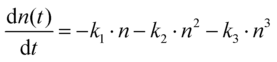
| Sample | k 1 (s−1) | k 2 (cm3 s−1) | k 3 (cm6 s−1) |
|---|---|---|---|
| CsPbBr3 | 4.09 × 10⁷ | 3.70 × 10⁻¹⁰ | 6.75 × 10⁻²⁸ |
| CsPbBr3–CsPb2Br5 | 2.30 × 10⁸ | 4.57 × 10⁻¹⁰ | 6.75 × 10⁻²⁸ |
Conclusion
In this work, we have demonstrated a scalable deposition method for creating uniform, crack-free, and flexible films consisting of perovskite MCs. Furthermore, we investigated how the implementation of the 2D CsPb2Br5 phase into CsPbBr3 microcrystals affects their structural and optical properties. Rietveld refinement confirms the presence of ∼20% of Pb-vacancies in the dual phase, which eventually increases the ion migration energy barrier, thereby promoting its stability. Corresponding proof-of-concept devices were tested for sensitivity upon X-ray illumination, and it was found that the dual-phase sample demonstrated improved X-ray detection at higher voltage regimes. This enhanced stability provides a promising avenue for future improvements in fast charge extraction and X-ray image resolution. Time-resolved photoluminescence measurements revealed a prolonged lifetime of the dual-phase sample due to the presence of shallow defects that slow down electron–hole recombination kinetics. THz measurements confirmed the presence of additional defects, as indicated by the partially reduced carrier mobility. This is beneficial at higher voltages as it prevents the accumulation of an excess of charges at the contacts. Moreover, the dual-phase CsPbBr3–CsPb2Br5 MCs exhibit a much lower dark current, linked to suppressed ion migration, which, in combination with the formed Pb-based defect states, prevents the building up of polarization in the device configuration. These findings suggest that the introduction of Pb-defects may not be as detrimental as expected and could potentially serve as an effective means to optimize X-ray detection, as well as other high-voltage demanding energy conversion applications.Author contributions
L. C. conducted most of the experiments and their analysis, assisted by R. V. B., and wrote the manuscript under the supervision of B. P. and E. D. J. V. completed the time-resolved spectroscopy. R. A. S. assisted in XRD Rietveld refinement and calculations of the lattice parameters. G. R. and L. S. analyzed the time-resolved spectroscopy data. H. Z. performed THz measurements and analysis under the supervision of H. I. W. and M. B. L. C. and D. V. performed X-ray sensitivity measurements. The research line presented in the manuscript was conceived by E. D.Conflicts of interest
The authors declare no competing financial interests.Acknowledgements
We thank Luc Struye for performing X-ray sensitivity measurements. The authors acknowledge financial support from the Research Foundation – Flanders (FWO Grant Number S002019N), FWO doctoral fellowships to L. C., J. V. and G. R., and a postdoctoral fellowships to B. P. (FWO Grant Numbers 1SA0821N, 11F3520N, 11C6922N and 1275521N). E.D. acknowledges financial support from the European Research Council (ERC Starting grant, 101117274 X-PECT) and the KU Leuven Internal Funds (grant numbers STG/21/010, C14/23/090, and CELSA/23/018). B. P. and R. A. S. acknowledge ESRF ID09 beamline scientist Dr Mikhail Kozhaev for his help during the X-ray scattering measurement.References
- D. Liu and T. L. Kelly, Nat. Photonics, 2014, 8, 133–138 CrossRef CAS.
- H. Wei, Y. Fang, P. Mulligan, W. Chuirazzi, H.-H. Fang, C. Wang, B. R. Ecker, Y. Gao, M. A. Loi, L. Cao and J. Huang, Nat. Photonics, 2016, 10, 333–340 CrossRef CAS.
- Q. Jiang, L. Zhang, H. Wang, X. Yang, J. Meng, H. Liu, Z. Yin, J. Wu, X. Zhang and J. You, Nat. Energy, 2017, 2, 16177 CrossRef CAS.
- M. A. Mahmud, T. Duong, J. Peng, Y. Wu, H. Shen, D. Walter, H. T. Nguyen, N. Mozaffari, G. D. Tabi, K. R. Catchpole, K. J. Weber and T. P. White, Adv. Funct. Mater., 2022, 32, 2009164 CrossRef CAS.
- H. Bhatia, B. Ghosh and E. Debroye, J. Mater. Chem. C, 2022, 10, 13437–13461 RSC.
- Q. Van Le, H. W. Jang and S. Y. Kim, Small Methods, 2018, 2, 1700419 CrossRef.
- L. Clinckemalie, D. Valli, M. B. J. Roeffaers, J. Hofkens, B. Pradhan and E. Debroye, ACS Energy Lett., 2021, 6, 1290–1314 CrossRef CAS.
- H. Wang and D. H. Kim, Chem. Soc. Rev., 2017, 46, 5204–5236 RSC.
- D. Pennicard, B. Pirard, O. Tolbanov and K. Iniewski, MRS Bull., 2017, 42, 445–450 CrossRef.
- M. Spahn, Nucl. Instrum. Methods Phys. Res., Sect. A, 2013, 731, 57–63 CrossRef CAS.
- A. Datta, Z. Zhong and S. Motakef, Sci. Rep., 2020, 10, 20097 CrossRef CAS PubMed.
- S. Kasap, J. B. Frey, G. Belev, O. Tousignant, H. Mani, J. Greenspan, L. Laperriere, O. Bubon, A. Reznik, G. DeCrescenzo, K. S. Karim and J. A. Rowlands, Sensors, 2011, 11, 5112–5157 CrossRef CAS PubMed.
- S. Kasap, Nat. Photonics, 2015, 9, 420–421 CrossRef CAS.
- A. Datta, J. Fiala and S. Motakef, Sci. Rep., 2021, 11, 22897 CrossRef CAS PubMed.
- G. Kakavelakis, M. Gedda, A. Panagiotopoulos, E. Kymakis, T. D. Anthopoulos and K. Petridis, Adv. Sci., 2020, 7, 2002098 CrossRef CAS PubMed.
- S. Kasap, J. B. Frey, G. Belev, O. Tousignant, H. Mani, L. Laperriere, A. Reznik and J. A. Rowlands, Phys. Status Solidi B, 2009, 246, 1794–1805 CrossRef CAS.
- J. Kang and L.-W. Wang, J. Phys. Chem. Lett., 2017, 8, 489–493 CrossRef CAS PubMed.
- J. Peng, C. Q. Xia, Y. Xu, R. Li, L. Cui, J. K. Clegg, L. M. Herz, M. B. Johnston and Q. Lin, Nat. Commun., 2021, 12, 1531 CrossRef CAS PubMed.
- W. Pan, B. Yang, G. Niu, K.-H. Xue, X. Du, L. Yin, M. Zhang, H. Wu, X.-S. Miao and J. Tang, Adv. Mater., 2019, 31, 1904405 CrossRef CAS PubMed.
- H. Zhao, J. Qiu, B. Hou, L. Yi, X. Qin and X. Liu, Adv. Opt. Mater., 2023, 11, 2202668 CrossRef CAS.
- J. Liang, C. Wang, Y. Wang, Z. Xu, Z. Lu, Y. Ma, H. Zhu, Y. Hu, C. Xiao, X. Yi, G. Zhu, H. Lv, L. Ma, T. Chen, Z. Tie, Z. Jin and J. Liu, J. Am. Chem. Soc., 2016, 138, 15829–15832 CrossRef CAS PubMed.
- J. B. Hoffman, A. L. Schleper and P. V. Kamat, J. Am. Chem. Soc., 2016, 138, 8603–8611 CrossRef CAS PubMed.
- A. F. Gualdrón-Reyes, S. J. Yoon, E. M. Barea, S. Agouram, V. Muñoz-Sanjosé, Á. M. Meléndez, M. E. Niño-Gómez and I. Mora-Seró, ACS Energy Lett., 2019, 4, 54–62 CrossRef PubMed.
- M. V. Kovalenko, L. Protesescu and M. I. Bodnarchuk, Science, 2017, 358, 745–750 CrossRef CAS PubMed.
- H.-C. Wang, Z. Bao, H.-Y. Tsai, A.-C. Tang and R.-S. Liu, Small, 2018, 14, 1702433 CrossRef PubMed.
- Y. Kim, E. Yassitepe, O. Voznyy, R. Comin, G. Walters, X. Gong, P. Kanjanaboos, A. F. Nogueira and E. H. Sargent, ACS Appl. Mater. Interfaces, 2015, 7, 25007–25013 CrossRef CAS PubMed.
- J. Shamsi, P. Rastogi, V. Caligiuri, A. L. Abdelhady, D. Spirito, L. Manna and R. Krahne, ACS Nano, 2017, 11, 10206–10213 CrossRef CAS PubMed.
- C. C. Stoumpos, C. D. Malliakas, J. A. Peters, Z. Liu, M. Sebastian, J. Im, T. C. Chasapis, A. C. Wibowo, D. Y. Chung, A. J. Freeman, B. W. Wessels and M. G. Kanatzidis, Cryst. Growth Des., 2013, 13, 2722–2727 CrossRef CAS.
- W. Zhai, J. Lin, C. Li, S. Hu, Y. Huang, C. Yu, Z. Wen, Z. Liu, Y. Fang and C. Tang, Nanoscale, 2018, 10, 21451–21458 RSC.
- J. Chen, Y. Fu, L. Samad, L. Dang, Y. Zhao, S. Shen, L. Guo and S. Jin, Nano Lett., 2017, 17, 460–466 CrossRef CAS PubMed.
- V. Drushliak and M. Szafrański, Inorg. Chem., 2022, 61, 14389–14396 CrossRef CAS PubMed.
- S. Bera, R. K. Behera and N. Pradhan, J. Am. Chem. Soc., 2020, 142, 20865–20874 CrossRef CAS PubMed.
- S. Ghosh, B. Pradhan, W. Lin, Y. Zhang, L. Leoncino, P. Chabera, K. Zheng, E. Solano, J. Hofkens and T. Pullerits, J. Phys. Chem. Lett., 2023, 14, 1066–1072 CrossRef CAS PubMed.
- Y. W. Woo, Y.-K. Jung, G. Y. Kim, S. Kim and A. Walsh, Discov. Mater., 2022, 2, 8 CrossRef.
- J. Yin, Z. Xu, Q. Hu, G. Teobaldi, L.-M. Liu and O. V. Prezhdo, J. Am. Chem. Soc., 2023, 145, 5393–5399 CrossRef CAS PubMed.
- X. Zhang, T. Zhu, C. Ji, Y. Yao and J. Luo, J. Am. Chem. Soc., 2021, 143, 20802–20810 CrossRef CAS PubMed.
- X. Tang, Z. Hu, W. Yuan, W. Hu, H. Shao, D. Han, J. Zheng, J. Hao, Z. Zang, J. Du, Y. Leng, L. Fang and M. Zhou, Adv. Opt. Mater., 2017, 5, 1600788 CrossRef.
- H. Zhang, Z. Gao, R. Liang, X. Zheng, X. Geng, Y. Zhao, D. Xie, J. Hong, H. Tian, Y. Yang, X. Wang and T.-L. Ren, IEEE Trans. Electron Devices, 2019, 66, 2224–2229 CAS.
- M. Keshavarz, E. Debroye, M. Ottesen, C. Martin, H. Zhang, E. Fron, R. Küchler, J. A. Steele, M. Bremholm, J. Van de Vondel, H. I. Wang, M. Bonn, M. B. J. Roeffaers, S. Wiedmann and J. Hofkens, Adv. Mater., 2020, 32, 2001878 CrossRef CAS PubMed.
- H. Zhang, F. Wang, Y. Lu, Q. Sun, Y. Xu, B.-B. Zhang, W. Jie and M. G. Kanatzidis, J. Mater. Chem. C, 2020, 8, 1248–1256 RSC.
- Y. Chai, Z. Juan, Y. Wu, Y. Liu and X. Li, ACS Appl. Electron. Mater., 2023, 5, 544–551 CrossRef CAS.
- K. Sakhatskyi, R. A. John, A. Guerrero, S. Tsarev, S. Sabisch, T. Das, G. J. Matt, S. Yakunin, I. Cherniukh, M. Kotyrba, Y. Berezovska, M. I. Bodnarchuk, S. Chakraborty, J. Bisquert and M. V. Kovalenko, ACS Energy Lett., 2022, 7, 3401–3414 CrossRef CAS PubMed.
- T. Takahashi, S. Watanabe, M. Kouda, G. Sato, Y. Okada, S. Kubo, Y. Kuroda, M. Onishi and R. Ohno, IEEE Trans. Nucl. Sci., 2001, 48, 287–291 CAS.
- H. Tsai, F. Liu, S. Shrestha, K. Fernando, S. Tretiak, B. Scott, D. T. Vo, J. Strzalka and W. Nie, Sci. Adv., 2020, 6, eaay0815 CrossRef CAS PubMed.
- S. E. J. O’Kane, G. Richardson, A. Pockett, R. G. Niemann, J. M. Cave, N. Sakai, G. E. Eperon, H. J. Snaith, J. M. Foster, P. J. Cameron and A. B. Walker, J. Mater. Chem. C, 2017, 5, 452–462 RSC.
- E. A. Duijnstee, V. M. Le Corre, M. B. Johnston, L. J. A. Koster, J. Lim and H. J. Snaith, Phys. Rev. Appl., 2021, 15, 014006 CrossRef CAS.
- Z. Wang, L. Zeng, T. Zhu, H. Chen, B. Chen, D. J. Kubicki, A. Balvanz, C. Li, A. Maxwell, E. Ugur, R. dos Reis, M. Cheng, G. Yang, B. Subedi, D. Luo, J. Hu, J. Wang, S. Teale, S. Mahesh, S. Wang, S. Hu, E. Jung, M. Wei, S. M. Park, L. Grater, E. Aydin, Z. Song, N. J. Podraza, Z.-H. Lu, J. Huang, V. P. Dravid, S. De Wolf, Y. Yan, M. Grätzel, M. Kanatzidis and E. Sargent, Nature, 2023, 1–3 CrossRef PubMed.
- R. Devanathan, L. R. Corrales, F. Gao and W. J. Weber, Nucl. Instrum. Methods Phys. Res., Sect. A, 2006, 565, 637–649 CrossRef CAS.
- M. Nikl, K. Nitsch, E. Mihóková, K. Polák, P. Fabeni, G. P. Pazzi, M. Gurioli, S. Santucci, R. Phani, A. Scacco and F. Somma, Phys. E, 1999, 4, 323–331 CrossRef CAS.
- X. Wu, X. Zhang, W. Yu, Y. Zhou, W. Wong, W. He, K. P. Loh, X.-F. Jiang and Q.-H. Xu, J. Mater. Chem. A, 2023, 11, 4292–4301 RSC.
- H. Zhang, X. Liu, J. Dong, H. Yu, C. Zhou, B. Zhang, Y. Xu and W. Jie, Cryst. Growth Des., 2017, 17, 6426–6431 CrossRef CAS.
- J. A. Steele, P. Puech, M. Keshavarz, R. Yang, S. Banerjee, E. Debroye, C. W. Kim, H. Yuan, N. H. Heo, J. Vanacken, A. Walsh, J. Hofkens and M. B. J. Roeffaers, ACS Nano, 2018, 12, 8081–8090 CrossRef CAS PubMed.
- M. Shi, G. Li, W. Tian, S. Jin, X. Tao, Y. Jiang, E. A. Pidko, R. Li and C. Li, Adv. Mater., 2020, 32, 2002137 CrossRef CAS PubMed.
- B. Wu, H. Yuan, Q. Xu, J. A. Steele, D. Giovanni, P. Puech, J. Fu, Y. F. Ng, N. F. Jamaludin, A. Solanki, S. Mhaisalkar, N. Mathews, M. B. J. Roeffaers, M. Grätzel, J. Hofkens and T. C. Sum, Nat. Commun., 2019, 10, 484 CrossRef CAS PubMed.
- Y. Shi, W. Zhao, Z. Ma, G. Xiao and B. Zou, Chem. Sci., 2021, 12, 14711–14717 RSC.
- F. Pan, J. Li, X. Ma, Y. Nie, B. Liu and H. Ye, RSC Adv., 2022, 12, 1035–1042 RSC.
- Y.-Q. Zhou, J. Xu, J.-B. Liu and B.-X. Liu, J. Phys. Chem. Lett., 2019, 10, 6118–6123 CrossRef CAS PubMed.
- R. E. Brandt, J. R. Poindexter, P. Gorai, R. C. Kurchin, R. L. Z. Hoye, L. Nienhaus, M. W. B. Wilson, J. A. Polizzotti, R. Sereika, R. Žaltauskas, L. C. Lee, J. L. MacManus-Driscoll, M. Bawendi, V. Stevanović and T. Buonassisi, Chem. Mater., 2017, 29, 4667–4674 CrossRef CAS.
- D. W. deQuilettes, S. Koch, S. Burke, R. K. Paranji, A. J. Shropshire, M. E. Ziffer and D. S. Ginger, ACS Energy Lett., 2016, 1, 438–444 CrossRef CAS.
- L. Qin, L. Wu, B. Kattel, C. Li, Y. Zhang, Y. Hou, J. Wu and W.-L. Chan, Adv. Funct. Mater., 2017, 27, 1704173 CrossRef.
- H. Shi, X. Zhang, X. Sun, R. Chen and X. Zhang, J. Phys. Chem. C, 2019, 123, 19844–19850 CrossRef CAS.
- R. Ulbricht, E. Hendry, J. Shan, T. F. Heinz and M. Bonn, Rev. Mod. Phys., 2011, 83, 543–586 CrossRef CAS.
- H. Zhang, E. Debroye, W. Zheng, S. Fu, L. D. Virgilio, P. Kumar, M. Bonn and H. I. Wang, Sci. Adv., 2021, 7, eabj9066 CrossRef CAS PubMed.
- H. Zhang, E. Debroye, J. A. Steele, M. B. J. Roeffaers, J. Hofkens, H. I. Wang and M. Bonn, ACS Energy Lett., 2021, 6, 568–573 CrossRef CAS.
- B.-E. Cohen, M. Wierzbowska and L. Etgar, Adv. Funct. Mater., 2017, 27, 1604733 CrossRef.
Footnote |
| † Electronic supplementary information (ESI) available. See DOI: https://doi.org/10.1039/d3tc01903a |
| This journal is © The Royal Society of Chemistry 2024 |