
 Open Access Article
 This Open Access Article is licensed under a
 Creative Commons Attribution 3.0 Unported Licence
Ultra-low lattice thermal conductivity driven high thermoelectric figure of merit in Sb/W co-doped GeTe†
Khasim Saheb
Bayikadi
 a,
Safdar
Imam
a,
Wei-Shen
Tee
b,
Sugumaran
Kavirajan
a,
Chiao-Yu
Chang
b,
Amr
Sabbah
bc,
Fang-Yu
Fu
d,
Ting-Ran
Liu
d,
Ching-Yu
Chiang
e,
Dinesh
Shukla
f,
Chien-Ting
Wu
g,
Li-Chyong
Chen
dh,
Mei-Yin
Chou
*b,
Kuei-Hsien
Chen
*bd and
Raman
Sankar
*a
a,
Safdar
Imam
a,
Wei-Shen
Tee
b,
Sugumaran
Kavirajan
a,
Chiao-Yu
Chang
b,
Amr
Sabbah
bc,
Fang-Yu
Fu
d,
Ting-Ran
Liu
d,
Ching-Yu
Chiang
e,
Dinesh
Shukla
f,
Chien-Ting
Wu
g,
Li-Chyong
Chen
dh,
Mei-Yin
Chou
*b,
Kuei-Hsien
Chen
*bd and
Raman
Sankar
*a
aInstitute of Physics, Academia Sinica, Nankang, Taipei, Taiwan 11529. E-mail: sankarraman@gate.sinica.edu.tw
bInstitute of Atomic and Molecular Sciences, Academia Sinica, Taipei 10617, Taiwan. E-mail: chenkh@pub.iams.sinica.edu.tw
cTabbin Institute for Metallurgical Studies, Tabbin, Helwan 109, Cairo 11421, Egypt
dCenter for Condensed Matter Sciences, National Taiwan University, Taipei 10617, Taiwan
eNational Synchrotron Radiation Research Center, Hsinchu City 30077, Taiwan
fUGC-DAE Consortium for Scientific Research, Indore 452001, India
gTaiwan Semiconductor Research Institute, Hsinchu Science Park, Hsinchu 300, Taiwan
hCenter of Atomic Initiative for New Materials, National Taiwan University, Taipei 10617, Taiwan
First published on 24th October 2024
Abstract
High thermoelectric performance is a material challenge associated mainly with the manipulation of lattice dynamics to obtain extrinsic phonon transport routes, which can make the lattice thermal conductivity (κlat) intrinsically low by introducing multiple scattering mechanisms. The present study shows that the lattice-strain-induced phonon scattering resulting from microstructural distortions in GeTe-based compounds can enable ultralow lattice thermal conductivity. The unusual lattice shrinkage, W interstitials, W nanoprecipitates, and heavy elemental mass, in Ge0.85Sb0.1W0.05Te culminate in an ultralow lattice thermal conductivity of ∼0.2 W m−1 K−1 at 825 K. Microstructural distortions in this Sb/W co-doped GeTe are found to be primarily associated with shorter W–Te bonding owing to the anomalous effect of the higher electronegativity of the W atoms. Furthermore, the increased electrical conductivity (σ) resulting from the enhanced vacancy formation caused by W doping and W interstitials synergistically contributes to optimization of the thermoelectric performance (ZT) to ∼2.93 at 825 K. The thermoelectric efficiency (η) as high as ∼17% has been obtained for a single leg in this composition at an operating temperature of 825 K, with an estimated device ZT value of ∼1.38.
Introduction
The growing global energy demand has increased the necessity for alternative energy technologies. Among the three alternative energy technologies (conversion, conservation, and storage), thermoelectric technology falls between the conversion and conservation categories. Energy conversion, such as from fuel to kinetic energy, dissipates a significant amount (two-thirds) of energy in the form of heat, which could be saved by using thermoelectric devices.1 Thermoelectric materials that are environmentally friendly can transform waste heat into energy, and such a solid material design should have optimum carrier transport and minimal thermal transit.2 The dimensionless figure of merit (ZT = S2σ/κT), which is largely responsible for improving thermoelectric performance, is governed by three material properties, namely, thermopower (S), electronic conductivity (σ), and thermal conductivity (κ = κele + κlat) contributed by the carrier (κele) and lattice (κlat).3 With effective scattering mechanisms, the ultimate ultralow lattice thermal conductivity (κlat) might be formulated, which can scatter broadly across all phonon spectrum frequencies (low, medium, and high).4,5 Materials with ground breaking performance need to be designed to provide whole phonon group scattering to achieve an ultralow κlat value, such as anisotropic behaviour in layered crystals,3 hierarchical nano/meso-scale structural design,4 creation of complex crystal structures,6 liquid crystalline behaviour,7,8 bond anharmonicity due to the presence of lone pairs,9 and co-doping of substituents with ionic behaviour.10Owing to its unique band structure, microstructures, grain boundaries, stacking faults, and point defects, GeTe has attracted much interest among mid-temperature thermoelectric compounds11 and has potential advantages over other well-known PbTe and SnSe thermoelectric compounds.3,12 Owing to its inherent vacancies, GeTe has a low impact on the immaculate performance, yet it has proven to be the best alloy compound among PbTe,13 SnTe,14 AgSbTe2,15 and Cu2Te–PbSe.16 GeTe-based compounds have been extensively explored in the past decade owing to their vacancy control for optimized carrier concentration (n) with various dopants, among which the best aliovalent cation dopants (such as Bi or Sb)17–20 continually reduce the carrier contribution to thermal conductivity (κele). However, an evident contribution to the lattice thermal conductivity (κlat) of ∼2.5–1.5 W m−1 K−1 at 300 K was confirmed using individually doped compounds. There is a large scope for reducing the lattice thermal conductivity (∼0.5–0.3 W m−1 K−1), which has been explored using multiple co-dopants including (Se–S),5 (Bi–In),18 (Bi–Pb),19 (Sb–Mn),21 (Sb–In),22 (Sb–Pb),23 (Sb–Cu),24 (Sb–Ti),25 (Sb–Cr),26 (Sb–Bi),27 (Bi–Mg),28 and (Sn–S–Se).29 Optimized carrier transport and thermal transport in doped-GeTe compounds have resulted in the highest thermoelectric performance (ZT) of ∼2.5–2.6 in the mid-temperature range (700 K), proving that GeTe compounds are some of the best thermoelectric materials.30,31
The entropy effect of a material is governed by its lattice dynamics, which reduces the lattice contribution to minimal thermal conductivity (κlat), improving the thermoelectric performance.29,30 GeTe with multiple dopants significantly reduces the κlat value by creating more disorder and a strained lattice that can enhance phonon scattering.5,21,27,29 Owing to the dominance of entropy-driven atomic disorders, a ternary system compound will always have a lower κlat value compared to a binary system compound.23,27,30 A strategic approach to vacancy control in GeTe32 and the strain-induced morphological boundary generated by Sb-doped GeTe20 has encouraged us to investigate co-substitution with heavy element tungsten (W). Comprehensive theoretical and experimental investigations were conducted to determine the impact of co-dopant W on the thermoelectric performance, focusing on the following questions: (a) Will W occupy the GeTe lattice? (b) What positions might W occupy in the GeTe lattice? (c) What is the maximum amount of W that can enter the GeTe lattice? (d) What microstructural changes can W cause? (e) How do substituted and interstitial W affect the transport properties of GeTe? (f) Does the nanoprecipitate contain phase-separated W? What are the primary effects of W in its various forms on κlat?
We investigated W-doped Ge0.9Sb0.1Te exhibiting an ultralow κlat value which led to higher thermoelectric performance and efficiency. To improve understanding, the ultralow κlat value and higher efficiency (η) of Ge0.85Sb0.1W0.05Te were explored, with the W co-dopant found to create an additional local band and large scattering centres, such as point defects, microstructural changes, strained herringbone domain boundaries, nanoprecipitates, and a disordered lattice and boundaries. Although it is well established that inhomogeneous internal-strain fields create phonon scattering centres, this research shows that internal-strain may also, on average, soften a material's lattice, hence altering sound velocity and phonon dispersion. Microstructural defects and internal strain, in addition to phonon scattering, allow for more control over lattice thermal conductivity. Overall, an optimized power factor of ∼36–38 μW m−1 K−2 and enhanced scattering have resulted in ultralow κlat values of ∼0.42 (325 K)–0.2 (825 K) W m−1 K−1, which correspond to the highest ZT values of ∼2.85–2.93 at 825 K. Thermoelectric efficiencies as high as ∼17% have been estimated for the p-type single leg device performance, with an average ZT value of ∼1.85 in the temperature range of 400–800 K.
Results
High-frequency phonons can be significantly dispersed by point defects in solid solutions owing to mass and strain changes between the host and guest atoms. Therefore, point defects with substantial mass and strain contrasts are advantageous for reducing the κlat value. However, the point defect density of solid solutions is limited by the solubility of the solutes.21,27,33 The large concentration of point defects in semiconductors with an intrinsically highly disordered crystal structure suggests that these might be promising thermoelectric materials.21 As a result, phonon scattering may be further amplified owing to the substantial mass and size difference between Sb/Ge and W/Ge atoms. To further investigate the thermoelectric properties of Ge0.85Sb0.1W0.05Te, we investigated its crystallographic features to determine whether a high ZT value could be obtained.The κlat value of Ge0.85Sb0.1W0.05Te diminishes to ∼0.2 W m−1 K−1 at 825 K, which is the lowest among known GeTe-based compounds, as shown in Fig. 1.18,34 The lattice contribution to the thermal conductivity (κlat) of GeTe, Ge0.9Sb0.1Te, and Ge0.85Sb0.1W0.05Te samples was calculated by subtracting the κele value from the κtotal value, with the κlat values shown in Fig. 1(a). The Cahill model, Clarke model, diffusion model, and Born–von Karman periodic boundary model have been used to derive the theoretical minimum κlat value of Ge0.85Sb0.1W0.05Te, with results of ∼0.47, 0.34, 0.29, and 0.19 W m−1 K−1, respectively. 4,34 These findings suggest that the experimental minimum κlat value for the present Sb/W co-doped materials is below the so-called glass limit, approaching the diffusion limit reported by Snyder.35 The observed κlat value of Ge0.85W0.05Sb0.1Te below 300 K was fitted using the Debye–Callaway model to better understand the effect of multiple phonon-scattering processes on the ultralow κlat value of Sb/W co-doped GeTe.4 The contribution of several scattering processes to the decreased κlat value of Ge0.85W0.05Sb0.1Te is shown in Fig. 1(b). The results indicated that Sb/W co-doping creates large strain fields and mass fluctuations, despite suppressing the κlat value.34
 | ||
| Fig. 1 (a) State-of-the-art reduction of lattice thermal conductivity (κlat) (inset, state-of-the-art systematic ZT enhancement); (b) the phonon–phonon Umklapp process (U), grain boundary scattering (B), point-defect scattering (PD), stacking fault scattering (SF), resonant phonon scattering (RES), nanoprecipitates (NPs), and microstructure scattering (MS) all contribute to the κlat value of Ge0.85Sb0.1W0.05Te. (c–f) Micro-to-nano-level phonon scattering mechanism of micro grain boundaries (B), herringbone microstructure (MS), domain boundaries (DB), and nanoprecipitates (NPs); and (g–j) nano-to-atomic-level phonon scattering mechanism of lattice disorder, stacking faults, point defects, and heavy mass with lattice shrinkage and charge effects. | ||
The total phonon scattering relaxation time, τ, can be expressed as follows:
 | (1) |
 | (2) |
Eqn (2) corresponds to the Debye–Callaway model representing the minimum κlat value for the GeTe system in Fig. 1(a) (dashed line). The κlat values of all samples decreased with increasing temperature. Furthermore, the addition of Sb and W decreased the κlat value significantly. GeTe had a κlat value of ∼2.43 W m−1 K−1 at 325 K, which was significantly reduced to ∼0.4 W m−1 K−1 for Ge0.85Sb0.1W0.05Te. Interestingly, GeTe co-doped with Sb and W showed a larger reduction in the κlat value compared with the controlled single-doped (Sb) GeTe samples (Fig. 1(a)). This significant reduction was attributed to synergistic phonon scattering caused by the observed 10–20 nm W nanoprecipitates and atomic-scale point defects resulting from mass fluctuations created by W replacing Ge in GeTe. W formed small nanoprecipitates in the GeTe matrix owing to the large size mismatch and solubility limit, while Sb preferred to form a solid solution in GeTe. Therefore, Sb and W have complementary roles in reducing the κlat value of GeTe. The overall micro-to-atomic scale phonon scattering mechanism is depicted in Fig. 1(c)–(j).
| τC−1 = τU−1 + τN−1 + τB−1 + τS−1 + τD−1 + τP−1 | (3) |
Eqn (3) shows the overall relaxation time, where τU, τN, τB, τS, τD, and τP are the relaxation times corresponding to scattering from Umklapp processes, normal processes, boundaries, strains, dislocations, and precipitates.4 Combining all the aforementioned scattering processes in the Ge0.85W0.05Sb0.1Te system significantly lowered the κlat value by ∼0.2 W m−1 K−1. The overall thermoelectric performance optimization studies are further discussed below.
Structural and elemental characterization
To confirm the bond length changes due to W substitution, we recorded the Fourier transformed EXAFS spectra for Ge0.9Sb0.1Te and Ge0.85Sb0.1W0.05Te samples. As observed in Fig. 2(a), it should be noted that the similarities in photoelectron backscattering of Sb and Te make distinction between Ge–Sb and Ge–Te bonds in EXAFS data difficult;36 thus, we focus only on Te EXAFS before and after introducing W. We can see the shortening of the bond length after W doping which can be attributed to the replacement of W with a Ge atom in the GST crystal system. The high-resolution TEM images of the Ge0.85Sb0.1W0.05Te sample in Fig. 2(b) clearly show W nanoprecipitation. The lattice changes due to W doping were confirmed by using Fast Fourier Transformation (FFT), shown in Fig. 2(b) and (c), revealing the GeTe (021) plane along with the existing W (200) plane. The lattice distance for the GeTe (021) plane dropped from ∼3.42 Å (rhombohedral) and ∼3.45 Å (cubic) to ∼3.38 Å for the Ge0.85Sb0.1W0.05Te compound because of W bonding to Te. Also, the presence of an additional dot represented the W cubic (200) plane (mp-1134) lattice distance of ∼2.48 Å, which originates from the nanoprecipitation.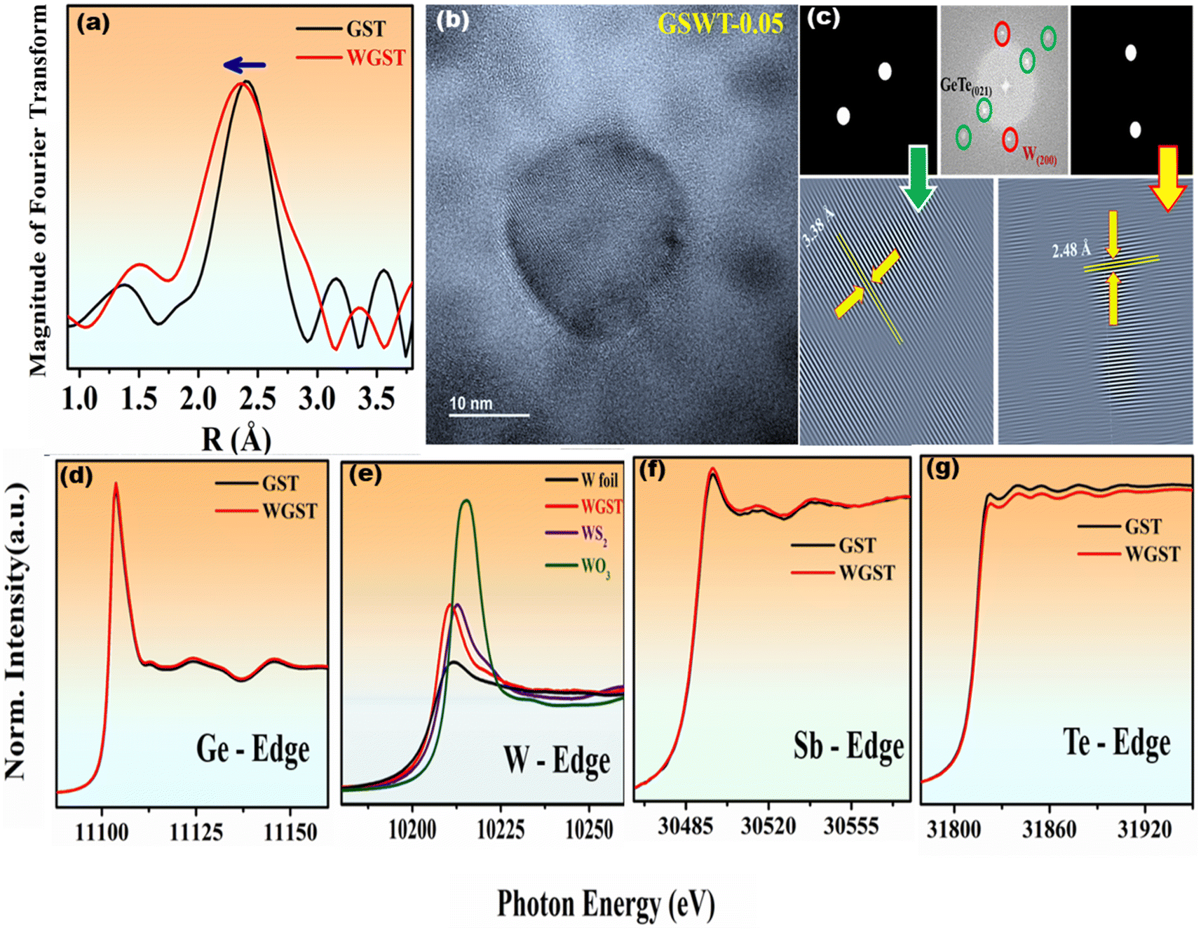 | ||
| Fig. 2 (a) Fourier transformed EXAFS spectra of the R space of ground pellets GST (black) and WGST (red), (b) HR-TEM image of W nanoprecipitated Ge0.85Sb0.1W0.05Te, and (c) Fast Fourier Transformation (FFT) with lattice analysis of the GeTe (021) plane and W (200) plane. (d) Experimental XANES spectra at the Ge K-edge for Ge0.9Sb0.1Te (black line) and Ge0.85Sb0.1W0.05Te (red line). (e) Experimental XANES spectra at the W L-edge for different-oxidation state W foil (0) (black line), Ge0.85Sb0.1W0.05Te (+2) (red line), WS2 (+4) (indigo line) and WO3 (+6) (green line). (f) Experimental XANES spectra at the Sb K-edge for Ge0.9Sb0.1Te (black line) and Ge0.85Sb0.1W0.05Te (red line). (g) Experimental XANES spectra at the Te K-edge for Ge0.9Sb0.1Te (black line) and Ge0.85Sb0.1W0.05Te (red line). | ||
We recorded X-ray absorption fine structure spectra for Ge0.9Sb0.1Te (GST) and Ge0.85Sb0.1W0.05Te (WGST) to learn more about their crystal structures and the atomic occupancy of doping elements. As can be seen in Fig. 2(d), when compared with the X-ray absorption near-edge structure (XANES) of the Ge K-edge, the XANES of the Ge K-edge of Ge0.9Sb0.1Te and Ge0.85Sb0.1W0.05Te shows hardly any difference between the two materials. Fig. 2(f) shows a comparison of the XANES spectra of the Sb K-edge in Ge0.9Sb0.1Te and Ge0.85Sb0.1W0.05Te. The behavior observed here was quite similar to that of the Ge K-edge. Since theoretical research shows that W-doping is predicted to reduce the bond length between Te and W atoms, XAS was used as a potent approach to analyse the local structure and determine how W doping affects the Te K-edge. Te K-edge absorption spectra of Ge0.9Sb0.1Te and Ge0.85Sb0.1W0.05Te are shown in Fig. 2(e). The electron densities of the Te K-edge XANES spectra clearly differ, demonstrating that W's high electronegativity significantly adjusts the Te bond length without producing a secondary phase telluride, confirming W doping at the Ge site. As shown in Fig. 2(g) tungsten L-edge X-ray absorption spectroscopy was used to probe a set of tungsten compounds covering the element's formal oxidation states from 0 to +VI.37 To put it another way, the excitation probability of the black line in the metal (0) is less than that in the oxide because the metal's conductive band is already filled with electrons. However, after W doping (Ge0.85Sb0.1W0.05Te), a change in intensity is still observed due to the increase in shared electron density, which is consistent with our theoretical findings. These spectra are helpful because their calculated correlations allow for an evaluation of the effective metal oxidation state (+2).37
The microstructural evolution was characterized using X-ray nano diffraction (XND) with a 90 × 90 nm2 spot size to map the grain orientation, grain shape, and grain size. As described in Fig. 3(b), orientation mapping was conducted on the yellow marked square in the SEM image of the pellet surface (Fig. 3(a)). Fig. 3(c) shows the inverse pole figure of the sample direction relative to the cubic system.38 The XND analysis revealed the orientations of the grains along the z direction in the sample pellet. The microstructure shows a bigger grain size as well as small fine grains which could be related to grains with enriched W ratios in accordance with the XRD results, particularly in areas where the W nanoprecipitates formed. For elemental distributions, we conducted an X-ray nanoprobe study to verify the existence of W at certain positions. The XRF maps (Fig. 3(e)) of the region indicated in the SEM image in Fig. 3(a) demonstrate near-uniform distribution of germanium, antimony, and tellurium within the scanning area. In contrast, tungsten shows a localized distribution along the grain boundaries. More specifically, we show the W spectrum in Fig. 3(f) of the region indicated in the intensity map image in Fig. 3(d). As shown in region 1, where there is no aggregation of W primarily in a big grain, the spectrum shows the presence of all 4 elements, with a low intensity of the W peak. However, in region 2, where the W precipitates are located, we can see a strong peak of W while Sb and Te are absent, indicating the presence of metallic W. On the other hand, region 3 shows the existence of all elements with a high ratio of W indicating the W precipitate along the small grains of Ge0.85Sb0.1W0.05Te as previously shown in the orientation map in Fig. 3(b).
 | ||
| Fig. 3 (a) SEM of surface topography of the polished pellet, (b) orientation mapping of the yellow marked square in the SEM image, (c) inverse pole figure based on the cubic phase, (d) intensity map of the yellow marked square in the SEM image, (e) XRF maps of the constituent alloying elements (Ge, Sb, Te, and W), and (f) XRF spectrum of the highlighted region of the intensity map figure (d). | ||
Microstructural analysis
Microstructural changes in vacancy-controlled GeTe, Sb-substituted GeTe, and W-doped GeTe were investigated theoretically and experimentally. The results of experimental and theoretical analyses of the GeTe, Ge0.9Sb0.1Te, and Ge0.85Sb0.1W0.05Te samples are shown in Fig. 4. Fig. 4(a)–(c) show the GeTe microstructure controlled by vacancies,32 Sb-substituted GeTe,20 and W-co-doped Ge0.85Sb0.1W0.05Te, respectively. Controlled Ge vacancies, as shown in Fig. 4(a), can reduce lattice shrinkage and enhance domain width. However, Ge vacancies can increase lattice shrinkage owing to the movement of neighbouring Te atoms towards the vacancy sites, as shown in Fig. 4(j), resulting in very narrow domains.32 The high- and low-intensity peaks that appear correspond to the atomic sizes of different atoms (Ge, Sb, W, and Te). Fig. 4(d)–(f) show HAADF-STEM images of vacancy-controlled GeTe and Ge0.85Sb0.1W0.05Te compounds. Fig. 4(d) shows vacancy-controlled pristine GeTe with a uniform distribution of atoms, while Fig. 4(e) shows Ge0.85Sb0.1W0.05Te with highly occupied atomic sites. These contrasts and variations in atomic sizes showed that Ge atoms were replaced with heavy Sb/W atoms.30Fig. 4(f) shows a clear lattice view of the Ge0.85Sb0.1W0.05Te compound with a small tilt in the sample, demonstrating the existence of lattice strain in the crystal plane of the system. As shown in Fig. 4(k), Sb-doping at Ge sites induced strain by pushing out neighbouring Te atoms. Fig. 4(g) shows the existing herringbone structure with additional strained boundaries arising from different types of additional strain, including (Sb and W substitution) along with possible W interstitials. Fig. 4(h) shows a magnified view of the strained boundary and the situated strained domains. Fig. 4(i) shows a magnified view of the strained domain located with a different lattice d-spacing owing to the persisting strains, as discussed in Fig. 4. Fig. S10† shows a highly magnified view of lattice distortions caused by the strain mechanism. The insets of Fig. S10† show the highly occupied and more disordered lattice arrangements. | ||
| Fig. 4 Transmission electron microscopy images of (a) vacancy-controlled GeTe, (b) Sb-doped GeTe, and (c) W-codoped Ge0.9Sb0.1Te. Analysis of herringbone domains and strained boundaries of Ge0.85Sb0.1W0.05Te: (d) herringbone domains and boundaries, (e) magnified view of domains and boundaries, and (f) atomic disorder in the domain lattice. High-angle annular dark-field (HAADF) scanning transmission electron microscopy (STEM) images of (g) GeTe, (h) Ge0.9Sb0.1Te, and (i) Ge0.85Sb0.1W0.05Te. Atomic movement of the neighbouring atoms driven by (j) a vacancy, (k) Sb substitution, and (l) W substitution. | ||
This strain was released at the end of each domain, establishing consecutive tensile and compressive strained boundaries.20,39 The present investigation of W-doping in Ge0.9Sb0.1Te imposed an additional strain owing to the higher Pauling electronegativity (∼2.36) of the W atom causing compression of its bond length with the Te atom, as shown in Fig. 4(l). This resulted in a shift in the microstructure from Ge0.9Sb0.1Te to Ge0.85Sb0.1W0.05Te, as shown in Fig. 5. The theoretical and experimental microstructural changes were virtually identical, including additional scattering of heavy element W point defects and strain contributing to the Ge0.85Sb0.1W0.05Te compound. As secondary confirmation, microstructural investigation showed that W entered the GeTe lattice.
 | ||
| Fig. 5 Density of states (DOS) for cubic GeTe systems with the following configurations: (a) pristine GeTe (black), and doped GeTe with W substitution (Ws, blue) and (c) interstitial W (Wi, red). The energy zero (dashed line) is defined by the top of the valence bands of pristine GeTe. The band energy in the doped cases is aligned with the bottom of the Te 5s states in pristine GeTe. Solid vertical lines indicate the Fermi levels of each doped system. Charge density distributions on W atom: (b) for substituted W (d) for interstitial W. | ||
Computational studies
We used first-principles simulations to investigate the function of W in GeTe. Based on ESI data,† we know that when W enters the GeTe structure, it occupies various sites. Table 1 summarizes the formation energies of W at various sites. In addition, W-doping may promote the formation of more Ge vacancies, which could lead to increased p-type doping (see Table 2).| W positions | W positions (with a Ge vacancy) | |||||
|---|---|---|---|---|---|---|
| Ws | Wi | (i) Ws | (ii) Ws | (iii) Wi | (iv) Wi | |
| Cubic | 2.79 | 2.91 | 2.52 | 1.94 | 2.28 | 2.24 |
| Rhombohedral | 3.10 | 3.12 | 2.54 | 2.10 | 2.03 | 1.96 |
| Ge vacancy | Ge vacancy (with a W atom) | ||
|---|---|---|---|
| Ws | Wi | ||
| Cubic | 0.27 | −0.58 | −0.40 |
| Rhombohedral | 0.56 | −0.44 | −0.60 |
Fig. 5 shows the theoretical investigation of spin–orbit coupling calculations, which revealed the band structure of pristine GeTe, W-doped GeTe, and W-interstitial GeTe compounds. Fig. S13† shows the partial density of states for pristine and W-interstitial GeTe compounds. Fig. S13(a)† shows the partial density of states for pristine GeTe, where the valence band (VB) is contributed by the Te p-orbitals and the conduction band (CB) is contributed by the Ge p-orbitals. The band structure of the W interstitials found in the GeTe compounds is shown in Fig. S13(b).† An increase in W interstitials will increase the number of local bands between the VB and CB, resulting in the generation of Ge vacancies, which ultimately enhances the metallic character of the system.
Fig. 5(a) shows the band structure of W-doped GeTe, where the Fermi level shifts from the VB to the CB, and some additional bands are generated from the W d-orbital. However, substitution with W atoms will decrease the formation of Ge vacancies, which eventually decreases the Fermi level further into the bandgap region. This shows that the W-doped GeTe system still maintained its p-type characteristic behaviour. In contrast, Fig. 5(b) shows charge density accumulation on the substituted W atom. Owing to their high electronegativity, the substituted W atoms will accumulate more charge density from the neighbouring Te atoms. Fig. 5(c) shows the W-substituted GeTe band structure, which shows the Fermi level shifting toward the CB with more interstitials. However, the theoretical calculations suggested that the possible Ge vacancies might further increase with W interstitials, eventually making the system more metallic in nature. Additional bands between the VB and CB were due to the contribution of W d-orbitals, but the calculated charge density distributions for W interstitials and neighbouring atoms were mostly localized, as shown in Fig. 5(d). These theoretical studies showed that the substituted and interstitial W atoms decreased the Ge vacancy formation energy and easily generated a higher carrier concentration (n) (holes) to contribute to charge transport. A more metallic character of the system was achieved due to the additional strain and defects introduced by the W atoms into the GeTe lattice, together with higher vacancy production. This increase in metallic nature and the effects of substitution, interstitials, and nanoprecipitates, on the system were further studied by investigating the temperature-dependent thermoelectric properties, which were in good agreement with the theoretical and microstructural effects.
Carrier transport studies
We investigated the temperature-dependent transport characteristics of electrical conductivity, Seebeck coefficient, and power factor using hot-pressed samples. Samples with a W-doping concentration of less than 2 atom% were prepared and their transport properties were examined to validate the W-doping concentration in the Ge sites. The temperature-dependent carrier transport features of low W concentration (x < 2 atom%) samples are shown in Fig. S14.† The temperature-dependent electrical conductivity (σ) of Ge0.9−xSb0.1WxTe samples (x = 0.0075–0.015) is shown in Fig. S14(a).† When W concentration was increased from 0.0075 to 0.1, the lowest σ value (580 S cm−1) was obtained at 325 K. Subsequent increases in the W concentration resulted in increased σ values. This trend in the σ value indicates that only a small quantity of W occupies the Ge sites, estimated to be approximately <1.5 atom%. For all samples, the σ value increased considerably after the phase transition (pseudo cubic to cubic phase, 525–625 K). The temperature-dependent Seebeck coefficient of Ge0.9−xSb0.1WxTe samples (x = 0.0075–0.015) is shown in Fig. S14(b).† The comparative S values of all samples showed favourable alignment of the VB (L and Σ) with more valleys, which contributed to the effective mass (m*), and heavy W doping reduced mobility (μ).22 Fig. S14(c)† shows the temperature-dependent power factor of Ge0.9−xSb0.1WxTe samples (x = 0.0075–0.015). Except for a W concentration of ∼1 atom%, all samples showed a power factor relatively comparable to that of pristine Ge0.9Sb0.1Te. The following results validated the doping limit concentration of W at the Ge sites, and the transport characteristics of samples with greater W concentrations were investigated further (2–6 atom%).The temperature-dependent charge transport properties of Ge0.9−xSb0.1WxTe samples (x = 0.02–0.06) are shown in Fig. 6(a)–(c). Fig. 6(a) shows the temperature dependent σ values of the samples. With increasing W concentration up to 4 atom%, the samples showed a systematic increase in σ values, while an abrupt increase was observed at a W concentration of 5 atom%. At 6 atom% W, the metallic nature of the system was enhanced. The metallic character of the samples supported the computational analyses. For the Ge0.84Sb0.1W0.06Te sample, a large increase in the σ value was observed. These results showed that the optimum limit of W in Ge0.9Sb0.1Te was <6 atom%, with the significant contribution to σ also accounting for the increase in the κele value in thermal transport. Fig. S15† shows the relationship between W concentration and carrier concentration (n) as well as mobility (μ). A systematic increase in the carrier concentration was clearly observed with increasing W concentration. At ∼6 atom% W, an enormous change was observed. More W incorporation enhanced the metallic nature of the Ge0.9Sb0.1Te system. The experimental results of carrier concentration (n) and σ values are shown in Table 3.
 | ||
| Fig. 6 (a–c) Temperature-dependent electronic transport properties of Ge0.9−xSb0.1WxTe compounds: (a) electrical conductivity (σ), (b) Seebeck coefficient (S) and (c) power factor (S2σ). (d–f) Thermal transport properties of Ge0.9−xSb0.1WxTe compounds: (d) total thermal conductivity (κtot), (e) lattice thermal conductivity (κlat), and (f) electronic thermal conductivity (κele). | ||
| Compound | n (×1020 cm−3) | μ (cm−2 V−1 s−1) | m* (me) | σ (S cm−1) | S (μV K−1) |
|---|---|---|---|---|---|
| GeTe | 7.33 | 70.54 | 1.28 | 8228 | 33 |
| Ge0.9Sb0.1Te | 0.84 | 68.74 | 1.15 | 927 | 121 |
| Ge0.89Sb0.1W0.01Te | 0.85 | 41.19 | 1.08 | 560.93 | 121.8 |
| Ge0.88Sb0.1W0.02Te | 1.07 | 54.38 | 1.25 | 932.27 | 120 |
| Ge0.87Sb0.1W0.03Te | 1.65 | 37.80 | 1.55 | 999.23 | 111.9 |
| Ge0.86Sb0.1W0.04Te | 2.4 | 26.26 | 1.98 | 1009.67 | 110.8 |
| Ge0.85Sb0.1W0.05Te | 4.0 | 21.39 | 2.43 | 1370.94 | 96.82 |
| Ge0.84Sb0.1W0.06Te | 8.5 | 22.87 | 2.52 | 3114.82 | 60.76 |
Fig. 6(b) shows the temperature-dependent Seebeck coefficient (S) of the Ge0.9−xSb0.1WxTe samples (x = 0.02–0.06). According to the Mott formula, an increase in the σ value always affects the S value because they are interconnected parameters, expressed as:
 | (4) |
Thermal transport studies
Fig. 6(d)–(f) show the temperature-dependent thermal transport properties of the Ge0.9−xSb0.1WxTe samples (x = 0.02–0.06). Fig. 6(d) shows the total thermal conductivity (κtot) of the samples. The overall thermal conductivity of the samples decreased with W doping of up to 4 atom%, while further increasing the W content resulted in an increase in thermal conductivity. For Ge0.86Sb0.1W0.04Te, the lowest thermal conductivity of ∼1 W m−1 K−1 was observed, while the sample with a W content of ∼0.06% showed the highest thermal conductivity of ∼1.75 at 775 K. Fig. 6(e) reveals the lattice-contributed thermal conductivity (κlat) calculated from κlat = κtot − κele. In describing heat transport, particularly when the chemical composition is affected, it is now believed that structural flaws predominantly reduce thermal conductivity via phonon scattering, impacting both phonon dispersion and speed of sound.40 Sound velocity is shown to decay linearly with increasing internal strain, as shown in Fig. S16† through experimental work on a GeTe compound system. This lattice softening, caused by the introduction of new phonon scattering mechanisms from nano and microstructural alterations and secondary heavy metal nanoprecipitates, is responsible for the overall decrease in lattice thermal conductivity.40,41 A systematic decrease in thermal conductivity was observed with an increasing W content inside the Ge0.9Sb0.1Te system. The lowest lattice thermal conductivities were observed for compositions with W contents of 0.05–0.06. The obtained lattice thermal conductivity values were between the limits of both theoretical models, namely, the Debye–Callaway model (0.4 W m−1 K−1) and Born–von Karman periodic boundary model (0.2 W m−1 K−1). 14,18,34,41 Fig. S17(d)† shows the measured thermal diffusivity (D). It is evident that co-doping with W along with Sb can significantly reduce thermal diffusivity (D). Furthermore, Fig. S17(d)† shows the measured specific heat (Cp) for Ge0.85Sb0.1W0.05Te compared with the Cp estimated using the Delong Petit law. As can be seen, the measured Cp varies within the error bar limit for all three batches of samples for heating and cooling cycles, and the Cp estimated using the Delong–Petit law approaches the average value of the measured results. Temperature independent ultra-low lattice thermal conductivity (κlat) was observed by Jiang et al.; the lattice softening as well as reductions in sound velocity will lead to ultra-low thermal conductivity.14,40–44 The lowest lattice thermal conductivity of ∼0.2 W m−1 K−1 was obtained for Ge0.85Sb0.1W0.05Te at 725–825 K.4,5,7,29 With the presence of point defects (Ge/Sb/W), stacking faults, nanoprecipitates, herringbone domains, domain boundaries, strained lattice, mass fluctuations, and twin domains, all existing scattering mechanisms will reduce the overall lattice thermal conductivity to the lower limit.4,10,18,27Fig. 6(f) shows the electronic contribution to the thermal conductivity of W co-doped Ge0.9Sb0.1Te samples. The electronic contribution to thermal conductivity is calculated from the Wiedemann–Franz law (κele = L0σT; L0, Lorentz number). The overall electronic contribution to the thermal conductivity increased with the increasing W concentration in the sample. The highest electronic contribution of ∼1.4 W m−1 K−1 was achieved for the Ge0.85Sb0.1W0.05Te sample at 775 K. Fig. S20† shows the lattice thermal conductivity (κlat) of GeTe-based compounds with different combinations of doping. Co-doping W with GeSbTe clearly reduces the lattice thermal conductivity to a minimum.State of the art: thermoelectric performance
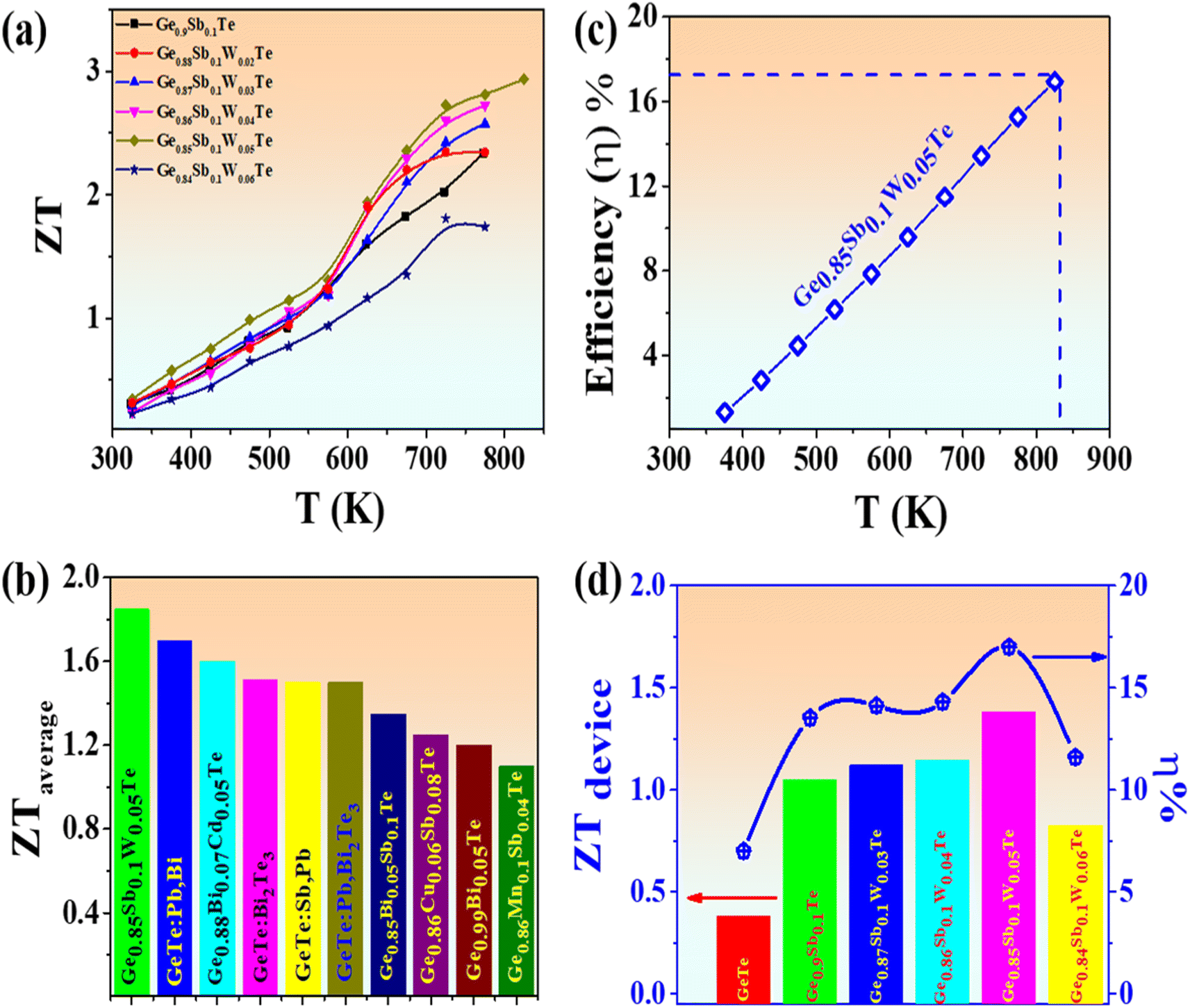
The high and stable ZT value of more than 2 realized in Ge0.9−xSb0.1WxTe largely originated from optimized carrier transport, along with the remarkable reduction in the κlat value caused by strategically induced lattice dynamic strains, boundaries, precipitates, and heavy point defects, resulting in more or less converged bands. Fig. 7(a) shows the overall thermoelectric performance of the W-doped Ge0.9Sb0.1Te compounds, with the overall highest ZT value of ∼2.93 at 825 K observed for Ge0.85Sb0.1W0.05Te. Fig. 7(b) shows the state-of-the-art average ZT enhancement compared with the highest values reported for GeTe-based compounds. The present system synergistically enhanced the average ZT value to 1.8 in the temperature range of 400–800 K. This is the highest ever reported average ZT value for any element-doped GeTe-based compounds. Fig. 7(c) shows the thermoelectric efficiency of the system in different temperature ranges. However, the efficiency of thermoelectric energy conversion (η) is largely determined by the material's average figure of merit :
: | (5) |
![[T with combining macron]](https://www.rsc.org/images/entities/i_char_0054_0304.gif) is the average temperature of Th and Tc, and
is the average temperature of Th and Tc, and  is the average figure-of-merit for each thermoelement (p- and n-type). Conventionally, the peak ZT value is used to evaluate the compatibility of thermoelectric materials with device applications. However, the peak ZT value does not guarantee high efficiency. To obtain a high-efficiency thermoelectric generator (TEG), the average
  value over the working temperature range is a more important parameter. The present compound exhibited the highest thermoelectric efficiency for a single leg, reaching 17% at 825 K.
 | (6) |
 | ||
| Fig. 7 (a) Temperature-dependent thermoelectric performance (ZT) of Ge0.9−xSb0.1WxTe compounds, (b) average ZT values of state-of-the-art GeTe-based compounds, (c) thermoelectric efficiency of Ge0.85Sb0.1W0.05Te compounds in the overall temperature range (325–825 K), and (d) state-of-the-art efficiency enhancement and device ZT values for GeTe compounds. | ||
Eqn (6) represents the device figure of merit.45,46Fig. 7(d) shows state-of-the-art materials, ranging from pristine GeTe to Sb-doped and W-doped GeTe systems, and the systematic increase in thermoelectric efficiency and device ZT values up to 5 atom% of W. Further incorporation of W might drastically reduce the device ZT value and efficiency owing to its highly metallic nature. Overall, the highest device ZT value of 1.38 and an efficiency of 17% were achieved using the Ge0.85Sb0.1W0.05Te compound. Moreover, the thermoelectric characteristics of Ge0.85Sb0.1W0.05Te exhibit excellent repeatability, and the ZT value remains consistent despite its uncertainty (Fig. S17†).
Conclusion
Theoretical strain inducement modelling, and experimental verifications together confirm that heavy element substitution-induced strain synergistically optimizes both electrical and thermal transport properties for achieving higher ZT, as demonstrated by W doping in the Ge0.9Sb0.1Te system. The current work investigated microstructural changes in Ge0.9−xWxSb0.1Te materials and their thermoelectric characteristics in detail. It is shown that the high electronegativity of W can induce an extraordinary strain due to a decreased bond length between W and Te atoms. The lattice dynamics are significantly altered by heavy element doping. Besides complexation, nanoprecipitation leads to highly crystalline strained domains and disordered boundaries. The doped GeTe compounds have lattice thermal conductivities of ∼0.4–0.2 W m−1 K−1, which correlate with their final ZT values. The entire phonon spectrum is screened out by heavy W point defects, strained domains with disordered boundaries, stacking faults, interstitials, nanoprecipitates, and surface defects, elevating the ZT values to ∼2.93 at 825 K. In the range of 400–800 K, the average ZT value achieved is higher than the reported value (∼1.8). With a device ZT value of ∼1.38 at 825 K, the anticipated single-leg efficiency is ∼17%, which is the highest among reported so far.Methods
Experimental procedure
Polycrystalline bulk samples of W co-doped Ge0.9Sb0.1Te were prepared by combining stoichiometric amounts of highly pure (99.999%) germanium (Ge), tellurium (Te), antimony (Sb), and tungsten (W) in quartz ampoules under a vacuum of 10−4 mbar. The samples were heated and melted at 973 K for 24 h and then cooled and crushed into extremely fine powders. The powders were then doubly sealed in quartz ampoules (to avoid compositional changes) and annealed at 1173 K for 48 h before quenching with air. The resulting ingots were ground into fine powder and then formed into high-density pellets by hot-press sintering at 820 K for 15 min under a vacuum of 10−5 mbar (to minimize oxidation) using a 15-mm graphite die under a pressure of 50 MPa. The Archimedes method was used to determine the densities of the heavily compressed pellets (∼98% of the theoretical density). To measure electrical and thermal transport characteristics, the pellets were chopped and polished into rectangular (12 × 3 × 3 mm3) or square pieces (6 × 6 × 2 mm3).Structural and chemical characterization
The presence of the secondary phase in the powder and hot-pressed pellet forms was validated by powder X-ray diffraction (PXRD) using a Bruker D8 diffractometer equipped with Cu Kα radiation (λ = 1.5406 Å). X-ray photoelectron spectroscopy (XPS) was performed using a PerkinElmer Physical Electronics PHI 5400 spectrometer equipped with a mono X-ray gun (Al) and a spherical electron energy analyzer with microscale X-ray focusing range capabilities. The carbon 1s peak at 284.6 eV was used to calibrate the XPS peak positions. Field-emission scanning electron microscopy (FESEM) with energy dispersive spectroscopy (EDAX) was used to confirm the elemental compositions (JEOL JSM-6700F). High-resolution transmission electron microscopy (HRTEM) was performed on the materials using Tecnai G2 F30 STWIN and JEOL JEM-ARM300F2TEM instruments, both equipped with a field emission gun capable of operating at 300 kV. X-ray absorption spectroscopy (XAS) was measured at beamline TLS 01C1 of the National Synchrotron Radiation Research Center facility in Taiwan. The Ge K-edge, Sb K-edge, and Te K-edge were recorded using transmission mode. The W L3-edge spectra were collected in fluorescence mode. The XANES spectra and EXAFS were plotted using the Athena program. GIWAXS was performed at beamline TLS 23A1. X-ray fluorescence spectroscopy (XRF) and orientation mapping were conducted using synchrotron nano diffraction (beamline 21A, Taiwan Photon Source (TPS)).Computational calculations
First-principles calculations were performed to investigate the doped GeTe systems. Vienna ab initio simulation software (VASP)47,48 with projector augmented wave (PAW) pseudo potentials was used. 49,50 The generalized gradient approximation (GGA)51 was used for the exchange-correlation functional. Different configurations in a 3 × 3 × 3 supercell of GeTe (originally 54 atoms) containing a W atom were considered. We used a plane-wave energy cutoff of 300 eV to ensure convergence. A Γ-centred 4 × 4 × 4 k-mesh for the supercell was adopted for self-consistent calculations, while a Γ-centred 8 × 8 × 8 k-mesh was used for density-of-states calculations. Spin–orbit coupling (SOC) was not included in atomic relaxation calculations but was included in all subsequent self-consistent calculations. The structure was fully relaxed using an energy criterion of 10−4 eV per cell between two steps. The VESTA program52 was used for structure visualization. We used the tetrahedron method with Blöchl corrections53 for Brillouin zone integration.Measurement of thermoelectric properties
The thermal diffusivity (D) and specific heat (Cp) of the sintered pellets were measured using the laser flash technique (LFA-457, NETZSCH) with reference to Pyroceram standard calibration and calculated using κ = DCpρ, whereas D, Cp, ρ and represents the thermal diffusivity, specific heat, and density, respectively. The electrical thermal conductivity (κele) was obtained using the Wiedemann–Franz law, κele = LσT, and the lattice thermal conductivity (κlat) was computed using the equation κlat = κtot − κele, where L is the Lorenz number calculated using the empirical formula , where S is the Seebeck coefficient. The thermal conductivity was believed to have a ±5% margin of error. The carrier transport characteristics were tested using a parallelepiped-shaped (3 × 2 × 15 mm3) pellet that was cut and polished in a helium gas environment, and S was measured concurrently on a ZEM-3 instrument (ULVAC), with the measurement accuracy estimated to be within ±5% for each parameter. In a magnetic field of up to 5 T, the Hall coefficient (Rh) was measured by the PPMS AC transport 5-point probe method. The carrier concentration (n) and mobility (μ) were calculated using the equations n = 1/(eRh) and μ = σRh, where e is the electron charge.
Data availability
The data supporting this article have been included as part of the ESI.†Conflicts of interest
The authors declare no conflicts of interest.Acknowledgements
The all authors gratefully acknowledge the AS-SS-113-01 Project funding for research on thermoelectric materials for sustainable energy. R. S. acknowledges the financial support provided by the Ministry of Science and Technology in Taiwan under Project No. NSTC-113-2124-M-001-003, No. NSTC-113-2112-M001-045-MY3, and No. NSTC113-2124-M-A49-003 as well as support from Academia Sinica for the budget of AS-iMATE-11312. R. S. and L.-C. C. acknowledges financial support from the Center of Atomic Initiative for New Materials (AIMat), National Taiwan University, and from the Featured Areas Research Center Program within the framework of the Higher Education Sprout Project by the Ministry of Education in Taiwan under Project No. 113L900801. The authors thank the National Synchrotron Radiation Research Center (NSRRC) team for the beamline of X-ray nanodiffraction (TPS 21A), Taiwan Photon Source (TPS).References
- J. Mao, H. Zhu, Z. Ding, Z. Liu, G. A. Gamage, G. Chen and Z. Ren, Science, 2019, 365, 495–498 CrossRef CAS PubMed.
- G. Tan, L.-D. Zhao and M. G. Kanatzidis, Rationally Designing High-Performance Bulk Thermoelectric Materials, Chem. Rev., 2016, 116, 12123–12149 CrossRef CAS PubMed.
- L. D. Zhao, S. H. Lo, Y. Zhang, H. Sun, G. Tan, C. Uher, C. Wolverton, V. P. Dravid and M. G. Kanatzidis, Ultralow thermal conductivity and high thermoelectric figure of merit in SnSe crystals, Nature, 2014, 508, 373–377 CrossRef CAS PubMed.
- K. Biswas, J. He, I. D. Blum, C. I. Wu, T. P. Hogan, D. N. Seidman, V. P. Dravid and M. G. Kanatzidis, Nature, 2012, 489, 414–418 CrossRef CAS PubMed.
- M. Samanta and K. Biswas, J. Am. Chem. Soc., 2017, 139, 9382–9391 CrossRef CAS PubMed.
- V. Dusastre, Materials for Sustainable Energy: A Collection of Peer-Reviewed Research and Review Articles from Nature Publishing Group, 2010, DOI:10.1142/7848.
- B. Li, H. Wang, Y. Kawakita, Q. Zhang, M. Feygenson, H. L. Yu, D. Wu, K. Ohara, T. Kikuchi, K. Shibata, T. Yamada, X. K. Ning, Y. Chen, J. Q. He, D. Vaknin, R. Q. Wu, K. Nakajima and M. G. Kanatzidis, Nat. Mater., 2018, 17, 226–230 CrossRef CAS PubMed.
- H. Liu, X. Shi, F. Xu, L. Zhang, W. Zhang, L. Chen, Q. Li, C. Uher, T. Day and G. Snyder Jeffrey, Nat. Mater., 2012, 11, 422–425 CrossRef CAS PubMed.
- D. T. Morelli, V. Jovovic and J. P. Heremans, Phys. Rev. Lett., 2008, 101, 035901 CrossRef CAS PubMed.
- A. A. Olvera, N. A. Moroz, P. Sahoo, P. Ren, T. P. Bailey, A. A. Page, C. Uher and P. F. P. Poudeu, Energy Environ. Sci., 2017, 10, 1668–1676 RSC.
- X. Zhang, Z. Bu, S. Lin, Z. Chen, W. Li and Y. Pei, Joule, 2020, 4, 986–1003 CrossRef CAS.
- Y. Wu, Z. Chen, P. Nan, F. Xiong, S. Lin, X. Zhang, Y. Chen, L. Chen, B. Ge and Y. Pei, Joule, 2019, 3, 1276–1288 CrossRef CAS.
- Z. Z. Luo, X. Zhang, X. Hua, G. Tan, T. P. Bailey, J. Xu, C. Uher, C. Wolverton, V. P. Dravid, Q. Yan and M. G. Kanatzidis, Adv. Funct. Mater., 2018, 28, 1801617 CrossRef.
- A. Banik, T. Ghosh, R. Arora, M. Dutta, J. Pandey, S. Acharya, A. Soni, U. V. Waghmare and K. Biswas, Energy Environ. Sci., 2019, 12, 589–595 RSC.
- S. H. Yang, T. J. Zhu, T. Sun, J. He, S. N. Zhang and X. B. Zhao, Nanotechnology, 2008, 19, 245707 CrossRef CAS PubMed.
- Z. Bu, X. Zhang, B. Shan, J. Tang, H. Liu, Z. Chen, S. Lin, W. Li and Y. Pei, Sci. Adv., 2021, 7, eabf2738 CrossRef CAS PubMed.
- X. Zhang, J. Li, X. Wang, Z. Chen, J. Mao, Y. Chen and Y. Pei, J. Am. Chem. Soc., 2018, 140(46), 15883–15888 CrossRef CAS PubMed.
- S. Perumal, M. Samanta, T. Ghosh, U. S. Shenoy, A. K. Bohra, S. Bhattacharya, A. Singh, U. V. Waghmare and K. Biswas, Joule, 2019, 3, 2565–2580 CrossRef CAS.
- D. Wu, L. D. Zhao, S. Hao, Q. Jiang, F. Zheng, J. W. Doak, H. Wu, H. Chi, Y. Gelbstein, C. Uher, C. Wolverton, M. Kanatzidis and J. He, J. Am. Chem. Soc., 2014, 136(32), 11412–11419 CrossRef CAS PubMed.
- K. S. Bayikadi, C. T. Wu, L. C. Chen, K. H. Chen, F. C. Chou and R. Sankar, J. Mater. Chem. A, 2020, 8, 5332–5341 RSC.
- Z. Zheng, X. Su, R. Deng, C. Stoumpos, H. Xie, W. Liu, Y. Yan, S. Hao, C. Uher, C. Wolverton, M. G. Kanatzidis and X. Tang, J. Am. Chem. Soc., 2018, 140(7), 2673–2686 CrossRef CAS PubMed.
- M. Hong, Z. G. Chen, L. Yang, Y. C. Zou, M. S. Dargusch, H. Wang and J. Zou, Adv. Mater., 2018, 30, 1705942 CrossRef PubMed.
- J. Li, X. Zhang, X. Wang, Z. Bu, L. Zheng, B. Zhou, F. Xiong, Y. Chen and Y. Pei, J. Am. Chem. Soc., 2018, 140(47), 16190–16197 CrossRef CAS PubMed.
- L. Xie, Y. Chen, R. Liu, E. Song, T. Xing, T. Deng, Q. Song, J. Liu, R. Zheng, X. Gao, S. Bai and L. Chen, Nano Energy, 2020, 68, 104347 CrossRef CAS.
- E. Nshimyimana, S. Hao, X. Su, C. Zhang, W. Liu, Y. Yan, C. Uher, C. Wolverton, M. G. Kanatzidis and X. Tang, J. Mater. Chem. A, 2020, 8, 1193–1204 RSC.
- M. Hong, K. Zheng, W. Lyv, M. Li, X. Qu, Q. Sun, S. Xu, J. Zou and Z. G. Chen, Energy Environ. Sci., 2020, 13, 1856–1864 RSC.
- S. Perumal, P. Bellare, U. S. Shenoy, U. V. Waghmare and K. Biswas, Chem. Mater., 2017, 29, 10426–10435 CrossRef CAS.
- T. Xing, Q. Song, P. Qiu, Q. Zhang, X. Xia, J. Liao, R. Liu, H. Huang, J. Yang, S. Bai, D. Ren, X. Shi and L. Chen, Natl. Sci. Rev., 2019, 6, 944–954 CrossRef CAS PubMed.
- P. Acharyya, S. Roychowdhury, M. Samanta and K. Biswas, J. Am. Chem. Soc., 2020, 142(48), 20502–20508 CrossRef CAS PubMed.
- T. Xing, C. Zhu, Q. Song, H. Huang, J. Xiao, D. Ren, M. Shi, P. Qiu, X. Shi, F. Xu and L. Chen, Adv. Mater., 2021, 33, 2008773 CrossRef CAS PubMed.
- Y. F. Tsai, P. C. Wei, L. Chang, K. K. Wang, C. C. Yang, Y. C. Lai, C. R. Hsing, C. M. Wei, J. He, G. J. Snyder and H. J. Wu, Adv. Mater., 2021, 33, 1–8 CrossRef PubMed.
- K. S. Bayikadi, R. Sankar, C. T. Wu, C. Xia, Y. Chen, L. C. Chen, K. H. Chen and F. C. Chou, J. Mater. Chem. A, 2019, 7, 15181–15189 RSC.
- J. W. Zhang, Z. W. Wu, B. Xiang, N. N. Zhou, J. L. Shi and J. X. Zhang, ACS Appl. Mater. Interfaces, 2020, 12, 21863–21870 CrossRef CAS PubMed.
- B. Shan, S. Lin, Z. Bu, J. Tang, Z. Chen, X. Zhang, W. Li and Y. Pei, J. Mater. Chem. A, 2020, 8, 3431–3437 RSC.
- M. T. Agne, R. Hanus and G. J. Snyder, Energy Environ. Sci., 2018, 11, 609–616 RSC.
- D. A. Baker, M. A. Paesler, G. Lucovsky, S. C. Agarwal and P. C. Taylor, Phys. Rev. Lett., 2006, 96, 255501 CrossRef CAS PubMed.
- U. Jayarathne, P. Chandrasekaran, A. F. Greene, J. T. Mague, S. Debeer, K. M. Lancaster, S. Sproules and J. P. Donahue, Inorg. Chem., 2014, 53(16), 8230–8241 CrossRef CAS PubMed.
- J. Cao, X. Y. Tan, N. Jia, D. Lan, S. F. D. Solco, K. Chen, S. W. Chien, H. Liu, C. K. I. Tan, Q. Zhu, J. Xu, Q. Yan and A. Suwardi, Nanoscale, 2022, 14, 410–418 RSC.
- H. S. Lee, B. S. Kim, C. W. Cho, M. W. Oh, B. K. Min, S. D. Park and H. W. Lee, Acta Mater., 2015, 91, 83–90 CrossRef CAS.
- R. Hanus, M. T. Agne, A. J. E. Rettie, Z. Chen, G. Tan, D. Y. Chung, M. G. Kanatzidis, Y. Pei, P. W. Voorhees and G. J. Snyder, Adv. Mater., 2019, 31, 1–10 CrossRef PubMed.
- B. Jiang, W. Wang, S. Liu, Y. Wang, C. Wang, Y. Chen, L. Xie, M. Huang and J. He, Science, 2022, 377, 208–213 CrossRef CAS PubMed.
- W. Li, S. Lin, B. Ge, J. Yang, W. Zhang and Y. Pei, Advanced Science, 2016, 3, 1600196 CrossRef PubMed.
- G. Tan, S. Hao, R. C. Hanus, X. Zhang, S. Anand, T. P. Bailey, A. J. E. Rettie, X. Su, C. Uher, V. P. Dravid, G. J. Snyder, C. Wolverton and M. G. Kanatzidis, ACS Energy Lett., 2018, 3, 705–712 CrossRef CAS.
- G. Xie, Z. Li, T. Luo, H. Bai, J. Sun, Y. Xiao, L. D. Zhao, J. Wu, G. Tan and X. Tang, Nano Energy, 2020, 69, 104395 CrossRef CAS.
- G. J. Snyder and A. H. Snyder, Figure of Merit ZT of a Thermoelectric Device Defined from Materials Properties, Energy Environ. Sci., 2017, 10, 2280 RSC.
- G. J. Snyder, Thermoelectric Power Generation: Efficiency and Compatibility, in Thermoelectrics Handbook: Macro to Nano, ed. D. M. Rowe, CRC Press, 2006, ch. 9 Search PubMed.
- G. Kresse and J. Furthmüller, Comput. Mater. Sci., 1996, 6, 15–50 CrossRef CAS.
- G. Kresse and J. Furthmüller, Phys. Rev. B: Condens. Matter Mater. Phys., 1996, 54(16), 11169–11186 CrossRef CAS PubMed.
- D. Joubert, Phys. Rev. B: Condens. Matter Mater. Phys., 1999, 59, 1758 CrossRef.
- P. E. Blöchl, Phys. Rev. B: Condens. Matter Mater. Phys., 1994, 50, 17953 CrossRef PubMed.
- J. P. Perdew and Y. Wang, Phys. Rev. B: Condens. Matter Mater. Phys., 1992, 45, 13244 CrossRef PubMed.
- K. Momma and F. Izumi, J. Appl. Crystallogr., 2011, 44, 1272–1276 CrossRef CAS.
- P. E. Blöchl, O. Jepsen and O. K. Andersen, Phys. Rev. B: Condens. Matter Mater. Phys., 1994, 49, 16223 CrossRef PubMed.
Footnote |
| † Electronic supplementary information (ESI) available. See DOI: https://doi.org/10.1039/d4ta05332j |
| This journal is © The Royal Society of Chemistry 2024 |