
 Open Access Article
 This Open Access Article is licensed under a Creative Commons Attribution-Non Commercial 3.0 Unported Licence
An X-ray detector with an ultra-low detection limit based on bulk two-dimensional perovskite PEA2PbBr4 single crystals grown in HBr solution†
Hao
Dong‡
 ab,
Xin
Liu‡
bc,
Hu
Wang
*bc,
Zhilong
Chen
bd,
Fenghua
Li
bc,
Pengxiang
Wang
bc,
Jie
Fu
ab and
Yuchuan
Shao
*abce
ab,
Xin
Liu‡
bc,
Hu
Wang
*bc,
Zhilong
Chen
bd,
Fenghua
Li
bc,
Pengxiang
Wang
bc,
Jie
Fu
ab and
Yuchuan
Shao
*abce
aSchool of Microelectronics, Shanghai University, Shanghai 201899, China. E-mail: shaoyuchuan@siom.ac.cn
bLaboratory of Thin Film Optics, Shanghai Institute of Optics and Fine Mechanics, Chinese Academy of Sciences, Shanghai 201800, China. E-mail: wanghu@siom.ac.cn
cCenter of Materials Science and Optoelectronics Engineering, University of Chinese Academy of Sciences, Beijing 100049, China
dKey Laboratory for Ultrafine Materials of Ministry of Education, Shanghai Engineering Research Center of Hierarchical Nanomaterials, School of Materials Science and Engineering, East China University of Science and Technology, Shanghai 200237, China
eSchool of Physics and Optoelectronic Engineering, Hangzhou Institute for Advanced Study, UCAS, Hangzhou 310024, China
First published on 28th September 2024
Abstract
Achieving a lower detection limit is always crucial for X-ray detectors in medical imaging. Two-dimensional (2D) perovskites are superior candidate materials for X-ray detection due to their high bulk resistivity, excellent environmental stability, and negligible ion migration under high bias. However, the reported detection limit of 2D perovskite X-ray detectors still apparently lags behind that of their 3D analogues due to the difficulty in the growth of high-quality bulk 2D perovskite single crystals (SCs). Herein, we demonstrate an X-ray detector with an ultra-low detection limit based on high-quality bulk PEA2PbBr4 SCs grown in HBr solution for the first time. According to the solubility difference of reactants, a slowly varying nucleation curve for the precursor solution is designed to stabilize growth rate and reduce defect density during crystal growth. The fabricated Au/PEA2PbBr4/Au detector shows a low noise level of 10−5 nA Hz−1/2 and an ultra-low dark current drift of 6.6 × 10⁻⁷ pA cm−1 V−1 s−1. Together with a commendable hole lifetime of 2.76 μs and hole mobility-lifetime product of 5.8 × 10⁻⁴ cm2 V−1, the produced detector exhibits a high sensitivity of 2998 μC Gyair s−1 cm−2 and a record-low detection limit of 0.79 nGyair s−1. The current work would be beneficial for the development of next generation medical imaging.
Introduction
Recent innovations in absorption materials have significantly enhanced the performance of X-ray detection technologies, driving ongoing research in this area. X-ray detectors are particularly important in fields such as medical diagnosis, civil security and military.1,2 These applications demand materials with specific properties, including high radiation absorption, efficient carrier transport and strong operational stability. In recent years, organic–inorganic hybrid perovskites have rapidly become a game changer for X-ray detectors due to their high average atomic number, low trap density, long carrier lifetime and high carrier mobility.3–8 Additionally, these perovskites exhibit strong self-healing ability after radiation damage, demonstrating high radiation tolerance.9–11 The first perovskite X-ray detector was based on three-dimensional (3D) perovskite polycrystalline films, demonstrating a sensitivity of 2500 μC Gyair−1 cm−2.12 Then single crystal (SC) perovskite detectors exhibit superior sensitivity due to the lower trap density and longer carrier diffusion lengths. These improved properties benefit from the absence of grain boundaries.13–15 Recently, a post-processed 3D MAPbI3 SC X-ray detector has achieved a significantly high sensitivity, reaching 700![[thin space (1/6-em)]](https://www.rsc.org/images/entities/char_2009.gif) 000 μC Gyair−1 cm−2 as reported.16 Moreover, detection limit is another critical parameter that assesses the signal-to-noise ratio level. A detector with a low detection limit is beneficial for low-dose detection to reduce medical injury. The mentioned 3D MAPbI3 SC X-ray detector has exhibited a low detection limit <10 nGyair s−1.16 However, 3D perovskites exhibit poor environmental stability, prone to decomposition in humidity, light and heat.17–19 Moreover, the gross ion migration in 3D perovskites leads to irreversible degradation, further compromising operational stability.20,21
000 μC Gyair−1 cm−2 as reported.16 Moreover, detection limit is another critical parameter that assesses the signal-to-noise ratio level. A detector with a low detection limit is beneficial for low-dose detection to reduce medical injury. The mentioned 3D MAPbI3 SC X-ray detector has exhibited a low detection limit <10 nGyair s−1.16 However, 3D perovskites exhibit poor environmental stability, prone to decomposition in humidity, light and heat.17–19 Moreover, the gross ion migration in 3D perovskites leads to irreversible degradation, further compromising operational stability.20,21
Compared to the structure AMX3 (A = MA+, FA+, or Cs+, M = a divalent metal cation, X = Cl−, Br− or I−) of 3D perovskites, Ruddlesden–Popper phase two-dimensional (2D) perovskites follow the general formula (R-NH3)2(A)n−1MnX3n+1, wherein R-NH3+ represents a long-chain monoammonium organic cation and n signifies the number of inorganic layers.22–24 The 2D perovskites feature a multiple quantum well structure composed of alternating organic and inorganic layers. The introduction of large organic ligands in 2D perovskites enhances environmental stability and suppresses ion migration.25–27 Moreover, the resistivity of 2D perovskites is typically two to three orders higher than that of 3D perovskites,28–30 which is preferable for achieving low noise current and detection limit for X-ray detection. However, the reported detection limit of 2D perovskite X-ray detectors still apparently lags behind that of their 3D analogues due to the difficulty in the growth of high-quality bulk 2D perovskite single crystals (SCs). For example, an (F-PEA)2PbI4 SC device and a [Cu(O2C-(CH2)3-NH3)2]PbBr4 SC device respectively exhibit detection limits of 23 nGyair s−1 and 56 nGyair s−1.28,29 Therefore, a crystal growth technique of 2D perovskite SCs to achieve a breakthrough in the detection limit is still worth developing.
Phenylethylamine (PEA+) generally serves as a passivating agent for 3D perovskites4,31 and functions as a common organic spacer for 2D perovskites.32,33 In direct X-ray detection, the fabricated PEA2PbBr4 thin-film detector demonstrated a sensitivity of 806 μC Gyair s−1 cm−2 and a detection limit of 42 nGyair s−1.34 It is worthy to investigate whether PEA2PbBr4 SCs could achieve a lower detection limit. Currently, in the limited number of cases where PEA2PbBr4 SCs have been grown in organic solvents,35–39 none of these crystals have been applied for direct X-ray detection. Meanwhile, Br-based perovskites have been shown to exhibit higher quality when grown in a halide-rich environment, such as hydrobromic acid (HBr).40,41 Reported PEA2PbBr4 substances obtained from HBr solution are in the form of nanosheets and platelets, lacking the bulk SC growth.40,42
Herein, we report the successful growth of bulk 2D PEA2PbBr4 SCs via temperature-lowering crystallization in HBr solution, using an optimized stoichiometric ratio of PEABr:PbBr2 = 2:3. The analysis of the precipitation curve confirms the need for excess PbBr2 to achieve a smoother nucleation process. Furthermore, high-quality crystal growth is achieved by maintaining a controlled, slow temperature-lowering process within an appropriate temperature range in a halide-rich environment. The maximum volume of PEA2PbBr4 SCs reaches 7 × 6 × 1 mm3. The thickness is sufficient for fabricating X-ray detectors with a vertical symmetrical electrode configuration, enabling effective absorption of X-ray photons. The produced PEA2PbBr4 SC detector shows negligible ion migration and a commendable carrier mobility–lifetime (μτ) product of 5.8 × 10⁻⁴ cm2 V−1 at room temperature, confirming the high quality of the SCs. With a high resistivity of 1.255 × 10¹² Ω cm, the detector exhibits good stability at high bias and a noise level as low as 10−5 nA Hz−1/2. This low noise ensures a stable and minimal dark current, ultimately yielding a record-low detection limit of 0.79 nGyair s−1. Moreover, the detector exhibits superior high sensitivity, reaching 2998 μC Gyair s−1 cm−2.
Experimental
Materials
Hydrobromic acid (HBr, 40 wt%) and lead bromide (PbBr2, 99%) were purchased from Aladdin Regent Ltd. 2-Phenylethylamine hydrobromide (PEABr, 99.5%) was purchased from Xi'an Yuri Solar Co., Ltd. All of these chemicals were used as received without further purification.Solubility measurement
The solubilities of individual solute and perovskite precursor in 40 wt% HBr were measured using the same installation as the SC growth. The nucleation temperatures of perovskite precursor solution with certain concentration were determined by temperature-lowering after dissolution at high temperature. Once recorded, the concentration was adjusted by adding solvent to obtain lower concentration for further test. The precipitation curves of solute with certain concentrations were determined by temperature-lowering after dissolution at a slight high temperature. The temperature point for solubility curves of perovskite precursor with certain concentrations were determined by temperature-raising.Synthesis of bulk PEA2PbBr4 SCs
The bulk PEA2PbBr4 SCs were grown in HBr solution using the STL method. PEABr (0.6 mmol) and PbBr2 (0.9 mmol) were dissolved in 15 mL of HBr. To dissolve the solute materials, the solution was heated to 95 °C and maintained at that temperature for 12 hours. It was then gradually cooled to 65 °C at a rate of 1 °C h−1, followed by further cooling to 25 °C at a rate of 0.1 °C h−1. Finally, the bulk PEA2PbBr4 single crystals were obtained.Device fabrication
The bulk PEA2PbBr4 SCs were fabricated into devices with a vertical structure along [001] direction. The carrier transport and extract also occurred along [001] direction in subsequent device characterization. Symmetry Au electrodes, with a thickness of 50 nm, were deposited by the evaporation method. A shadow mask was employed to create an electrode with dimensions of 2 × 2 mm2, representing the effective area of the device.Material characterization
Powder X-ray diffraction (XRD) measurements were conducted employing an X-ray diffractor (PANalytical Empyrean) with Cu Kα radiation. XRD rocking curve was measured using a high-resolution X-ray diffractometer (Bruker D8 Discover). Scanning electron microscopy (SEM) images were obtained using field emission scanning electron microscope (FESEM, Carl Zeiss). Atomic force microscope (AFM) analysis was carried out using a Bruker Dimension-3100. Thermogravimetric analysis was conducted on a TA SDT-Q600 instrument. The transmittance spectrum was recorded using a UV/vis/NIR spectrometer (PerkinElmer Lambda 1050). Photoluminescence (PL) and time-resolved photoluminescence (TRPL) spectra were acquired utilizing a laser-scanned fluorescence intensity/lifetime imaging system (FLRM, Time-Tech Spectra, LLC) with an excitation wavelength of 405 nm. Ultraviolet photoelectron spectroscopy (UPS) measurement was conducted on an X-ray photoelectron spectrometer (ThermoFischer, ESCALAB 250Xi). The UPS data were normalized to the range of 1 to 100.Device characterization
The current–voltage and current–time curves were mainly obtained using a source meter (Keithley 2634B) at room temperature. The temperature-dependent conductivity was obtained using the same source meter and cryogenic equipment (JANIS ST-LN-500-1) at varied temperature, controlled by temperature controller (Cryocon 22C). The temporal response was performed under the excitation of a 365 nm light-emitting diode modulated with a square wave at a fixed frequency of 5 Hz, controlled by a waveform generator (Keysight 33500B). The signals were collected and filtered at 30 Hz using a preamplifier (Stanford Research System, SR570) and recorded with an oscilloscope (Keysight MSO-X3104A). Hole mobility measurement was conducted by illuminating the devices with 337 nm laser pulses (SRS NL100). The pulse laser generated weak photocurrent was amplified by a preamplifier (Stanford Research System, SR570) and then recorded by an oscilloscope (Keysight MSO-X3104A). Photoconductivity measurements were conducted using the same LED source and waveform generator. Noise current was measured employing a spectrum analyzer (Stanford Research System, SR770 FFT Network Analyzer) in conjunction with the SR570 preamplifier. The X-ray source utilized is an Amptek MiniX2 tube featuring a silver (Ag) target, operated at a constant acceleration voltage of 30 kV. Control of the X-ray dose rate was achieved by adjusting both the tube current and the number of aluminum sheets positioned between the X-ray source and the detector. The X-ray dose rate was calibrated using an ion chamber dosimeter (Radcal AccuGold). A stainless-steel mask with a 2 × 2 mm2 hollow was consistently positioned above the device during X-ray performance measurement. Sensitivity (S) was determined using equation S = Isignal/AD, where Isignal represents the difference between the average photocurrent and average dark current, A is the effective area, and D is the X-ray dose rate. Signal-to-noise (SNR) was calculated as SNR = Isignal/Inoise, with Inoise denoting the standard deviation of the photocurrent.43Results and discussion
Growth of the bulk PEA2PbBr4 SC
Br-based perovskites synthesized in HBr exhibit superior environmental stability and a higher photoluminescence quantum yield compared to those synthesized in organic solvents.41 This enhancement is generally attributed to the passivation of halogen vacancy defect states in the halide-rich environment.40 Herein, we endeavor to grow PEA2PbBr4 SCs in 40 wt% HBr solution. According to the solution-based crystal growth theory, the saturation state of the precursor solution is crucial to control the crystallization process. The initial homogeneous nucleation generally takes place in supersaturation, while the growth process is situated between the nucleation and dissolution zones.44 Moreover, a reasonable temperature interval and a slowly varying nucleation curve for the precursor solution are crucial factors to provide a stable growth rate and reduce defect density during the growth process.42,45Here, a standard stoichiometric ratio of PEABr:PbBr2 = 2:1 in HBr is prepared as the precursor solution to grow bulk PEA2PbBr4 SCs. The corresponding temperature-dependent nucleation curve of the precursor solution is measured (details in the Experimental section) and shown in Fig. S1.† The nucleation concentration declines as the temperature decreases, which indicates that a solution temperature-lowering (STL) method is preferred. The STL method allows for precise control over the nucleation and growth process by gradually lowering the temperature of the solution. This helps in achieving high-quality single crystals with fewer defects. Moreover, the temperature control program can be tailored to different solubility curves.14,46 However, the measured nucleation curve exhibits a steep slope, especially for the higher temperature. Such a steep slope would significantly hinder the stable growth of bulk PEA2PbBr4 SCs. To optimize the temperature-dependent nucleation curve of the precursor solution, the temperature-dependent precipitation curve for an individual solute in HBr is measured. As shown in Fig. 1a, the slopes of the precipitation curve for both PEABr and PbBr2 are similar, indicating that a reasonable stoichiometric ratio of PEABr:PbBr2 in HBr could provide a relatively stable, temperature-dependent nucleation curve for the precursor solution. The composition of the precursor solution in the initial state greatly influences the stability and nucleation barrier during crystal growth. Since the precipitation concentration of PbBr2 is about 3 times higher than that of PEABr at the higher temperature, an excess of PbBr2 is required to balance the solubility differences for co-precipitation. Consequently, the chemical amount of PbBr2 is increased to 3 times the original amount for the following experiments. The temperature-dependent nucleation curve of the precursor solution with a stoichiometric ratio of PEABr:PbBr2 = 2:3 in HBr is measured as shown in Fig. 1b. The slope of the nucleation curve for the precursor solution of PEABr:PbBr2 = 2:3 is much smaller, which indicates the more stable growth process for the crystallization of bulk PEA2PbBr4 SCs. The nucleation zone, growth zone, and dissolution zone are summarized in Fig. 1c for the precursor solution of PEABr:PbBr2 = 2:3 according to the nucleation and dissolution curves.
 | ||
| Fig. 1 Growth of PEA2PbBr4 SCs. (a) Solubilities of PbBr2 and PEABr in HBr. (b) Nucleation curves of PEA2PbBr4 precursors with solute ratios of PEABr:PbBr2 = 2:3 and 2:1 in HBr. (c) Solubility and nucleation curve of PEA2PbBr4 grown in HBr with the solute ratio of PEABr:PbBr2 = 2:3. (d) Growth apparatus and temperature-controlled growth process. (e) Photograph of the fragile PEA2PbBr4 SC and bulk PEA2PbBr4 SC with the thickest grid of 1 cm2. | ||
The schematic diagram of the growth apparatus and process for the bulk PEA2PbBr4 SC is shown in Fig. 1d. The glass plate and silicone oil help to uniformly heat the precursor solution in a bottle. Based on the growth zone measured in Fig. 1c, the initial concentration of the precursor solution is set at 0.02 mol L−1 to ensure a sufficient growth range for prolonged and stable growth, enabling the formation of large-sized SCs. The corresponding growth temperature throughout the entire process remains below 100 °C, which is beneficial for safety. Before adjusting the temperature, the precursor solution is maintained at a constant temperature of 95 °C for 12 hours to ensure complete dissolution. Subsequently, the cooling process involves two steps: relatively rapid cooling at 1 °C h−1 from 95 °C to 65 °C for step 1, followed by slow cooling at 0.1 °C h−1 from 65 °C to 25 °C for step 2. Step 1 serves as a transitional phase, while step 2 is the main period for crystal growth. The entire procedure spans approximately 20 days, resulting in the attainment of bulk PEA2PbBr4 SCs with a thickness of around 0.8 mm. The maximum volume of the bulk PEA2PbBr4 SC can reach 7 × 6 × 1 mm3 as shown in Fig. 1e. In contrast, the PEA2PbBr4 SCs grown from a precursor solution with a stoichiometric ratio of PEABr:PbBr2 = 2:1 are mechanically fragile (using the same growth process with an initial concentration of 0.04 mol L−1). This growth characteristic highlights the challenge of growing bulk SCs. The fragile PEA2PbBr4 SCs have a thickness of around 0.1 mm, as shown in Fig. 1e and S2,† making them unsuitable for device processing and X-ray absorption. As shown in Fig. S3,† PEA2PbBr4 exhibits a linear attenuation coefficient comparable to those of CdZnTe and MAPbBr3. To absorb 90% of photons with 30 keV energy, the thickness of the PEA2PbBr4 SC needs to reach 0.68 mm. While the fragile PEA2PbBr4 SC cannot achieve this, the bulk PEA2PbBr4 SC provides sufficient thickness for effective photon absorption.
The powder X-ray diffraction (XRD) patterns of bulk PEA2PbBr4 in the upper part of Fig. 2a depict primary diffraction peaks corresponding to the (00l) planes of the layered structure. The peak positions of PEA2PbBr4 grown with a precursor solute ratio of PEABr:PbBr2 = 2:3 are consistent with those of PEA2PbBr4 grown with a precursor solute ratio of PEABr:PbBr2 = 2:1 in the lower part of Fig. 2a. Both patterns with different solute ratios align well with the calculation.47 This consistency confirms that the modified precursor solute ratio exhibits a negligible effect on the pure phase of PEA2PbBr4 crystals. A rocking curve analysis, presented in Fig. 2b, shows that the full-width at half-maximum (FWHM) of the (002) peak is as narrow as 0.027°. This small FWHM confirms the high quality of the bulk PEA2PbBr4 SC. The structure of PEA2PbBr4 is depicted schematically in Fig. 2c. As a 2D perovskite, PEA2PbBr4 features lead bromide octahedral sheets segregated by organic spacers of PEA+ cations. This arrangement is crucial for obtaining advantages such as high bulk resistivity and low ion migration. Simultaneously, the water stability and lattice hardness are improved by introducing large hydrophobic organic cations (PEA+).17 Scanning electron microscopy (SEM) is a widely used analytical technique for characterizing the surface topography of SCs. The top-view SEM image appears flat. When combined with the cross-sectional SEM image, the two images confirm the 2D layered structure of the PEA2PbBr4 SC, as shown in Fig. 2d.35,38 The cross-sectional image reveals a visible layer at the micron scale, which consists of multiple molecular-scale layers. Furthermore, the Atomic Force Microscopy (AFM) image in Fig. 2e and S4† reveals a flat plane within a 5 × 5 μm2 scale. The root mean square roughness (Rq) of 9.19 nm attests to the low surface roughness of these SCs, showing again the high crystal quality.
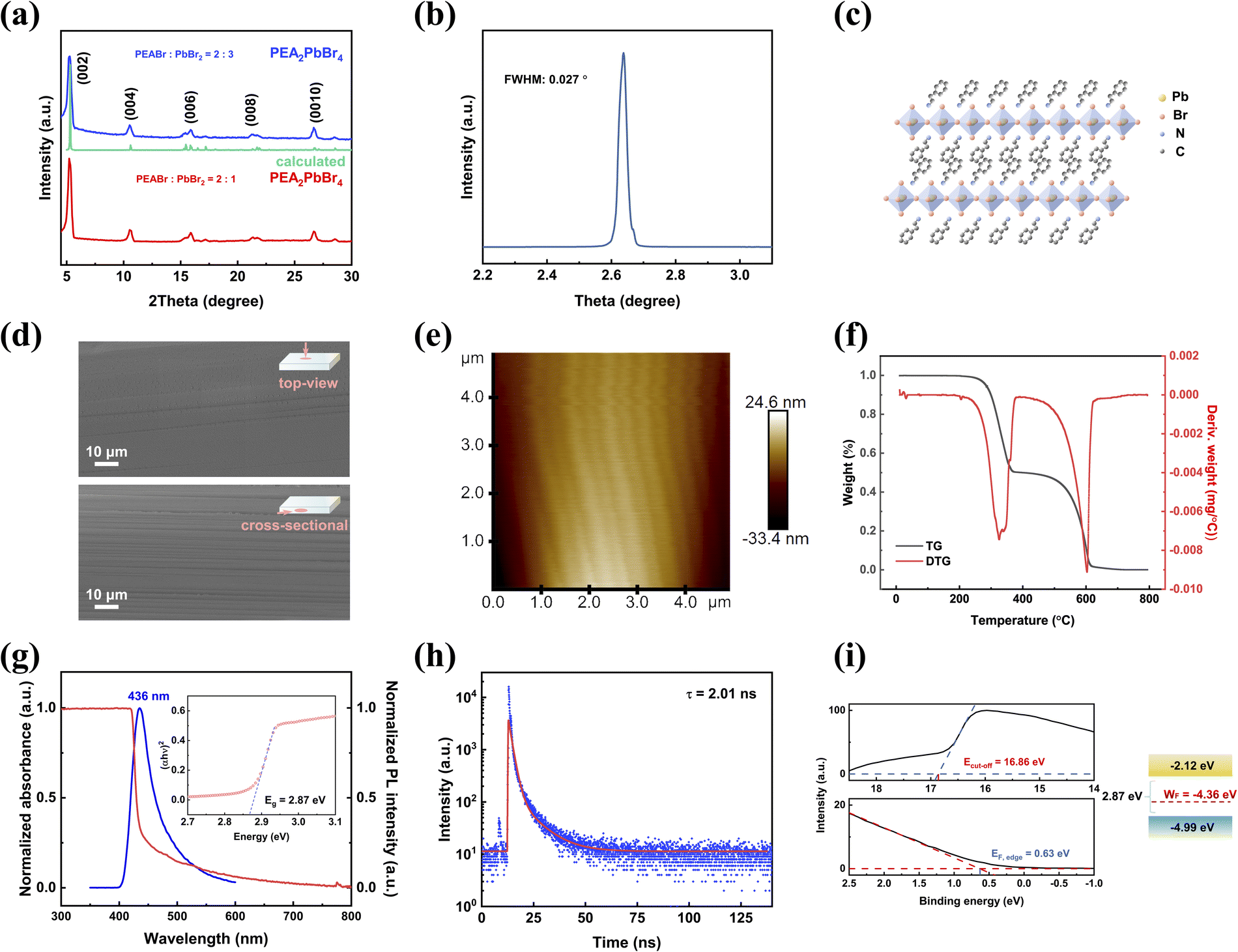 | ||
| Fig. 2 Characterization of the PEA2PbBr4 SC. (a) The powder XRD patterns of the PEA2PbBr4 SC with different precursor ratios. (b) The rocking curve of the (002) lattice plane of a PEA2PbBr4 SC. (c) Structural configuration of PEA2PbBr4. (d) The top-view and cross-sectional SEM images of the PEA2PbBr4 SC. (e) The AFM image of the PEA2PbBr4 SC. (f) Thermogravimetry curve and corresponding first derivative for the PEA2PbBr4 SC. (g) Normalized absorbance and photoluminescence spectrum of the PEA2PbBr4 SC (the inset shows the Tauc band gap of the PEA2PbBr4 SC). (h) Time-resolved photoluminescence decay curves of the PEA2PbBr4 SC using 400 nm excitation. (i) UPS spectrum and energy level diagram of the PEA2PbBr4 SC. | ||
As shown in Fig. 2f, the thermogravimetric (TG) curve of bulk PEA2PbBr4 SC powder shows that the initial point of mass loss happens at 230 °C, indicating the high thermal stability. This initial decomposition point corresponds to the previous report of PEA2PbBr4 SCs grown in an organic solution.38 Subsequently, the optical properties are analyzed through spectral characterization. The absorbance and photoluminescence (PL) spectra of the PEA2PbBr4 SC are obtained, as shown in Fig. 2g. The SC shows an absorption band extending to 420 nm, consistent with previous reports.37 The calculated optical bandgap of PEA2PbBr4 is found to be 2.83 eV, extracted from Tauc plots. The PL spectrum exhibits a single fluorescence peak at 436 nm under 400 nm excitation, indicating the pure phase of the PEA2PbBr4 SC. Notably, the asymmetric PL spectrum, with a low-energy tail, aligns with previous reports. This peak shape has been attributed to multiple exciton states, exciton–phonon interactions, and well-state radiative recombination, which are influenced by quantum and dielectric confinement effects.35 The fast lifetime of PEA2PbBr4 is measured at 2.01 ns by fitting the decay curve under the same excitation as shown in Fig. 2h. This short lifetime is attributed to the high exciton binding energy of the 2D perovskite.33 As shown in the left of Fig. 2i, the ultraviolet photoelectron spectroscopy (UPS) data are measured. Due to the obstacle in electron emission owing to the high resistivity of the bulk PEA2PbBr4 SC, a slow ascent occurs before the sharp cut-off in UPS. The Ecut-off (cut-off binding energy) was found to be 16.86 eV according to the cut-off region, which is similar to the reported PEA2PbBr4 SC.38 The work function (WF) of the PEA2PbBr4 SC could be calculated as −4.36 eV using the formula WF = Ecut-off − 21.22 eV.48 Then the valence band maximum (VBM) could be calculated as −4.99 eV using the formula VBM = WF − EF,edge, in which EF,edge refers to the Fermi edge. Eventually, considering that the measured bandgap is 2.87 eV, the energy level diagram of PEA2PbBr4 could be obtained as shown in the right of Fig. 2i. The WF of the PEA2PbBr4 SC is below the middle of the bandgap, indicating that PEA2PbBr4 SC is a p-type semiconductor, where holes in PEA2PbBr4 are the dominant carriers.
Out-of-plane electrical properties of the bulk PEA2PbBr4 SC
The large organic spacer significantly restricts ion migration in the out-of-plane direction, thereby minimizing dark current drift and reducing noise fluctuations.29 While the in-plane electrical properties of the PEA2PbBr4 SC have been studied in a previous report,38 our focus is on the out-of-plane electrical properties of the PEA2PbBr4 SC. Consequently, all subsequent measurements are oriented along the [001] direction. To examine the out-of-plane electrical properties and carrier transport behaviour of the bulk PEA2PbBr4 SC, we fabricated a device with Au electrodes on opposite sides via vacuum evaporation, as shown in the left of Fig. 3a. Each electrode measured 2 × 2 mm2 with a thickness of 50 nm. The corresponding energy level diagram of this structure is shown on the right side of Fig. 3a. Au is a reasonable electrode with its WF of −5.1 eV, which is close to the VBM of the PEA2PbBr4 SC, thereby facilitating hole transport. In Fig. 3b, the resistivity is recorded at 1.255 × 10¹² Ω cm, aligning with similar 2D perovskites listed in Table S1,†28–30 yet it surpasses classic 3D perovskites (such as CsPbBr3 and MAPbBr3) by one to three orders of magnitude.1,49 The high resistivity contributes to a device with minimal dark current and low noise, which is essential for an ionizing radiation detector. Additionally, the loop scanning demonstrates a low hysteresis, as shown in Fig. 3c. Most current differences are within 6 pA at identical voltage points between the forward and backward scans. The maximum current difference of 9.5 pA occurs at 194 V. This low hysteresis suggests that the 2D structure results in negligible ion migration.50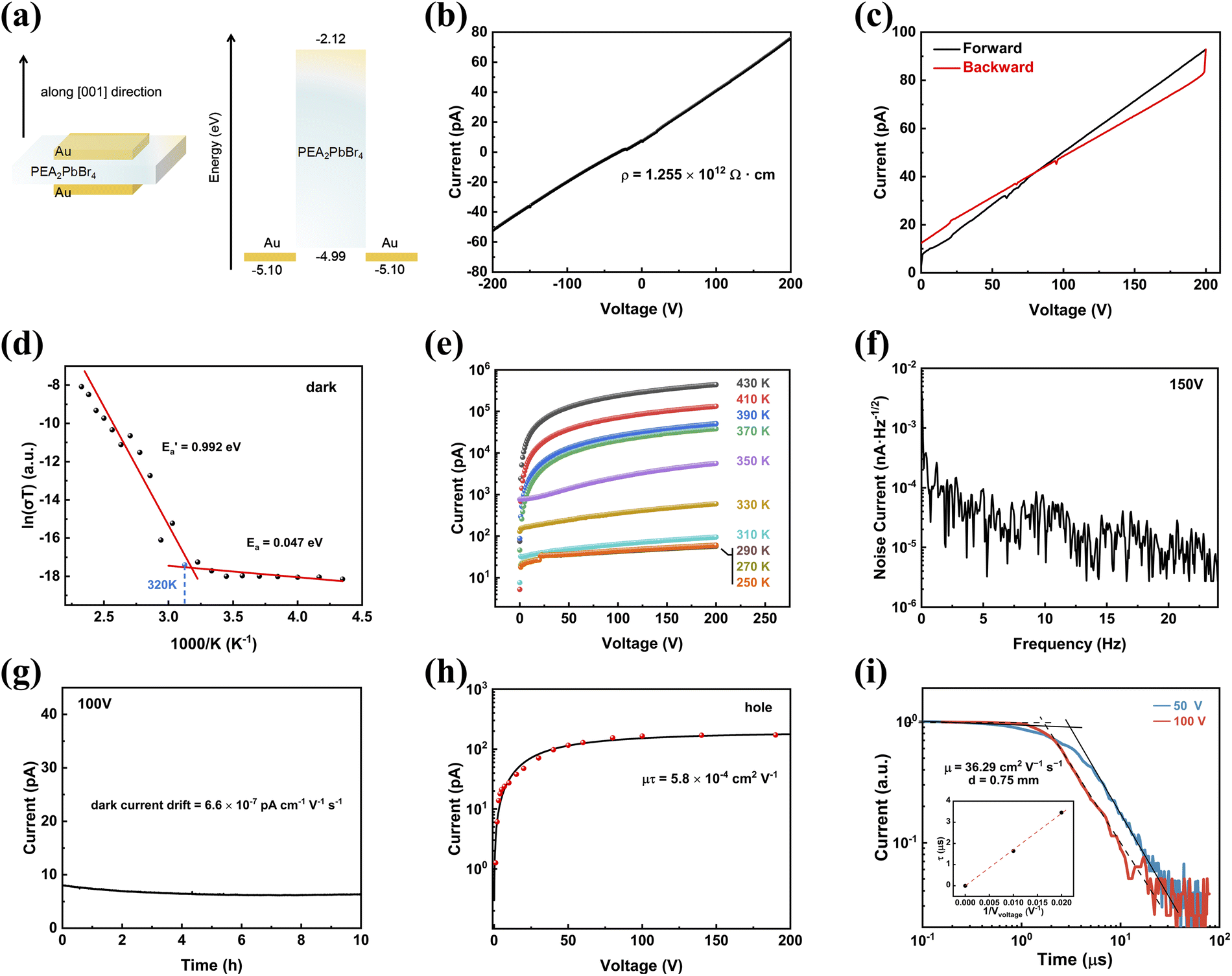 | ||
| Fig. 3 Out-of-plane electrical properties along the [001] direction of the PEA2PbBr4 SC. (a) Schematic illustration and corresponding energy level diagram of the device structure of Au/PEA2PbBr4/Au. (b) Current–voltage curve (∼1.7 V s−1 scanning rate). (c) Current–voltage hysteresis (∼1.7 V s−1 scanning rate). (d) Temperature-dependent conductivities of the PEA2PbBr4 SC device. (e) Current–voltage curves at various temperatures (∼1.7 V s−1 scanning rate). The curves for 250 K, 270 K and 290 K overlap. (f) Noise current spectra of the PEA2PbBr4 SC device. (g) Long-term dark current stability of the PEA2PbBr4 SC device at 100 V. (h) Photoconductivity measurement for holes under 0.13 mW cm−2 continuous ultraviolet LED (365 nm) illumination. (i) Normalized transient current curves of PEA2PbBr4 SC devices at 50 V and 100 V (the inset of (i) shows the charge transit time versus the reciprocal of bias). | ||
The performance of X-ray detection is greatly influenced by a stable dark current. The ion migration is a factor that predominantly affects current stability under operation. The lower ion migration of 2D perovskites benefits from the path-blocking induced by organic spacers and higher generation energy of ionic vacancies.51Fig. 3d illustrates the extraction of activation energy (Ea) through linear fitting of the plot ln(σT) − 1000/T, where T is the temperature and σ is the temperature-dependent conductivity under dark conditions.52,53 Two fitting regions are observed, yielding an Ea for low temperature in the range of 230 K to 320 K and an  for high temperature between 320 K and 430 K. The Ea at low temperature is associated with electronic conduction, whereas the
  at higher temperature serves as an energy barrier for ion migration.54,55 The bulk PEA2PbBr4 SC exhibits an
  of 0.992 eV, surpassing that of BA2PbBr4.30 The current–voltage curves, which correspond to the temperature-dependent conductivities, show the current stability at various temperatures as shown in Fig. 3e. Notably, below 310 K, the overlapped curves demonstrate that the bulk PEA2PbBr4 SCs device could operate stably without accumulation of ion migration effects caused by the measurement history. Moreover, the noise current spectra of the bulk PEA2PbBr4 SC device in Fig. 3f exhibit an ultra-low level of 10−5 nA Hz−1/2 at a high bias of 150 V, attributed to the substantial bulk resistivity and minor interface trap of the device,56 thereby enhancing the overall stability of the current. This low noise current shows a reduction by two to three orders of magnitude compared to the 3D MAPbBr3 SC device, although the bias applied on the PEA2PbBr4 SC device is 15 times more than that on the MAPbBr3 SC device.38 The long-term stability of dark current is shown in Fig. 3g. The drift of the dark current is 6.6 × 10⁻⁷ pA cm−1 V−1 s−1 over a 100 V bias for 10 hours.
The μτ product is a crucial parameter determining the carrier collection efficiency of the device. We simply observed the photo response of the PEA2PbBr4 SC vertical device (Fig. S5†) and further verified that the device demonstrates a favorable response to the 365 nm light-emitting diode (LED) source at various voltages, with detailed parameter settings provided (Fig. S6†). As expected, the dark current remains low and stable. Additionally, the bulk PEA2PbBr4 SC device exhibits higher hole current compared to electron current. Therefore, unless otherwise specified, the subsequent analysis refers to hole currents.
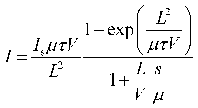
By subtracting the average dark current from the average photocurrent, the signal current data points were obtained, as shown in Fig. S7.† These data points were then used to derive the photoconductivity measurement, as shown in Fig. 3h. The photocurrent gradually saturates with increasing applied voltage, reaching saturation at approximately 65 V. The μτ product is determined through fitting the signal current–voltage curves by the modified Hecht equation:57
Carrier mobility is a significant factor that is conducive to achieving a high μτ product.60 The hole mobility of the PEA2PbBr4 SC is measured by the time of flight (TOF) method under a 337 nm laser pulse (Fig. 3i). The measured transit time is proportional to the reciprocal of the applied bias, and the carrier mobility is calculated from the slope divided by the square of the thickness. The hole mobility of the bulk PEA2PbBr4 SC reaches 36.29 cm2 s−1 V−1, which slightly exceeds the value of 31.3 cm2 s−1 V−1 observed in the (F-PEA)2PbI4 SC. 28 However, the higher μτ product compared with the (F-PEA)2PbI4 SC indicates the higher carrier lifetime. The hole lifetime of the bulk PEA2PbBr4 SC is further calculated to be 1.6 μs. Although this lifetime is two orders of magnitude smaller than the best reported value of 296 μs within 3D perovskite SCs, it is still one order higher than the lifetime of the CdZnTe (Cd0.9Zn0.1Te) SC. 61 Therefore, the low noise, high μτ product, hole mobility and hole lifetime demonstrate the high quality of the bulk PEA2PbBr4 SC with a low defect level.
The temporal response is defined as the time required for transition from 10% to 90% or 90% to 10% of two states of the two equilibrium current states. Benefiting from the superior carrier transport properties, the quick temporal response of the on/off current under 0.56 mW cm−2 light (365 nm) in pulse wave is presented with an on-response time of 32 ms and an off-response time of 36 ms, as shown in Fig. S9.† This response is provided as a limited sample, as it is significantly influenced by the frequency of the light source and the short measurement time, unlike other steady-state current measurements. The applied 365 nm LED is modulated with a square wave at a fixed frequency of 5 Hz. A reported PEA2PbBr4 SC ultraviolet detector has also shown a faster temporal response <1 ms with the working frequency of 167 Hz, showing the high performance of the PEA2PbBr4 photodetector.38
X-ray performance of the bulk PEA2PbBr4 SC detector
Continuing with the same vertical device structure featuring symmetrical 50 nm Au, we further investigate the X-ray performance at a bias of 100 V under 30 keV X-ray. Fig. 4a presents measurements of the X-ray response across dose rates ranging from 118.4 nGyair s−1 down to 3.682 nGyair s−1. Radiation response decreases as the dose rate decreases, which is consistent with the general rule. To further analyze the X-ray performance of the PEA2PbBr4 SC device at 100 V, the X-ray responses with dose rates from 118.4 to 3.682 nGyair s−1 are presented in Fig. S10.† With the dose rate of 118.74 nGyair s−1, 48.74 nGyair s−1 and 3.682 nGyair s−1, the X-ray responses of the bulk PEA2PbBr4 SC detector are illustrated as typical examples in Fig. 4b. The stable currents show the feasibility of operating with low dose rates and demonstrate that the PEA2PbBr4 SC device could perform under high voltage conditions with good tolerance. Notably, the device still exhibits a distinguishable on–off response with an ultra-low dose rate of 3.682 nGyair s−1, as shown in Fig. 4b. This response performance indicates the potential for high sensitivity and a low detection limit.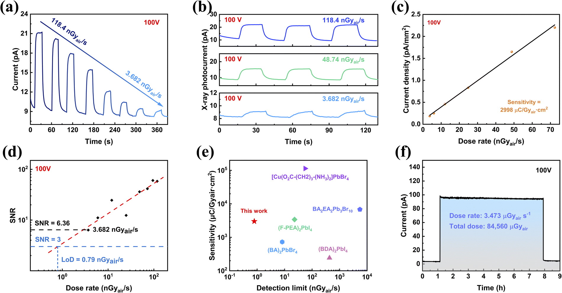 | ||
| Fig. 4 X-ray performance along the [001] direction of the PEA2PbBr4 SC detector at a bias of 100 V. (a) X-ray responses to different dose rates of the PEA2PbBr4 SC detector. (b) Three on–off X-ray responses of the PEA2PbBr4 SC detector with three dose rates. (c) X-ray photocurrent density with different dose rates, the sensitivity is obtained by fitting the current density–dose rate. (d) SNR of the PEA2PbBr4 SC detector. (e) The comparison of the sensitivities and detection limits based on the 2D perovskite SC detectors. (f) Operational stability of the PEA2PbBr4 SC detector with X-ray off–on–off. | ||
Sensitivity is one of the critical parameters for X-ray detectors, reflecting the ability to directly convert X-ray radiation into current signal. The sensitivity of the bulk PEA2PbBr4 SC detector at 100 V is determined to be 2998 μC Gyair s−1 cm−2 by the slope of the linear fitting of current density–dose rate (Fig. 4c). This value is 150 times higher than that of the commercial stabilized a-Se detector and 1.74 times higher than that of the (o-F-PEA)2PbI4 SC (1724.5 μC Gyair s−1 cm−2@1250 V mm−1).62,63 The bulk PEA2PbBr4 SC detector exhibits such high sensitivity by extracting carriers at a high bias of 100 V, which benefits from the high voltage tolerance.
Furthermore, we assess the detection limit of the bulk PEA2PbBr4 SC detector. The detection limit is another critical parameter that corresponds to the dose rate at which the signal-to-noise ratio reaches 3.64 Low detection limit will result in the detector exhibiting low-dose detection for low medical injury. As a result of linear fitting, the device achieves an ultra-low detection limit of 0.79 nGyair s−1 at 100 V as illustrated in Fig. 4d. The corresponding on–off responses at 100 V are depicted in Fig. S10.† As mentioned before, detection limit reflects the level of signal-to-noise ratio. Thus, this ultra-low detection limit arises from the high μτ product and low noise, where the low noise ensures a stable and minimal dark current. The detection limit of 0.79 nGyair s−1 marks a rare small value for both 2D and 3D perovskite X-ray detectors. A comparison of the performance between reported 2D perovskite SC-based detectors and our Au/PEA2PbBr4/Au detectors is summarized in Fig. 4e and Table S1.†28–30,46,48,65 The detection limits of some typical 3D perovskite X-ray detectors are listed in Table S2.†
Finally, to examine the operational stability under X-ray exposure, the PEA2PbBr4 SC device was subjected to continuous X-ray radiation with a dose rate of 3.473 μGyair s−1 for approximately 7 hours, between two periods in a dark environment without X-ray radiation (Fig. 4f). Throughout the entire process, the device maintains an ultra-stable current at a bias of 100 V. The range of the X-ray photocurrent (the difference between maximum and minimum values) is 0.57 pA.
Conclusions
In summary, we demonstrate the growth of high-quality bulk PEA2PbBr4 SCs using the STL method in HBr based on a slowly varying nucleation curve. The growth rate is stabilized to enable the high-quality SC growth with a low defect level. The substantial bulk resistivity of the PEA2PbBr4 SC results in a low and stable dark current, showing the promising advantages for an X-ray detector. After being processed into a device with symmetrical Au electrodes, the PEA2PbBr4 SC device exhibits good stability at high voltages. A high hole lifetime of 2.76 μs confirms the high-quality of the PEA2PbBr4 SC and facilitates the achievement of a high μτ product of 5.8 × 10⁻⁴ cm2 V−1 and a high sensitivity of 2998 μC Gyair s−1 cm−2 at 100 V. Moreover, benefiting from the high μτ product and low noise, the fabricated device achieves a rare low detection limit of 0.79 nGyair s−1. This work will provide a guidance for growing high-quality 2D perovskite SCs in HBr solution and designing X-ray detectors based on 2D perovskite SCs.Data availability
The authors confirm that the data supporting the findings of this study are available within the article and its ESI.†Author contributions
Hao Dong: conceptualization, methodology, writing – original draft & review & editing; Xin Liu: investigation, methodology, writing – review; Zhilong Chen, Fenghua Li, Pengxiang Wang and Jie Fu: investigation, methodology; Hu Wang: conceptualization, funding acquisition, writing – review; Yuchuan Shao: funding acquisition.Conflicts of interest
There are no conflicts to declare.Acknowledgements
This work was supported by the National Natural Science Foundation of China (62104234), and the Shanghai Explorer Program (22TS1400100).Notes and references
- H. Wei and J. Huang, Nat. Commun., 2019, 10, 1066 CrossRef PubMed.
- Z. Chen, H. Wang, F. Li, W. Zhang, Y. Shao and S. Yang, ACS Appl. Mater. Interfaces, 2023, 15, 51370–51379 CrossRef CAS PubMed.
- L. Clinckemalie, D. Valli, M. B. J. Roeffaers, J. Hofkens, B. Pradhan and E. Debroye, ACS Energy Lett., 2021, 6, 1290–1314 CrossRef CAS.
- L. Chen, H. Wang, W. Zhang, F. Li, Z. Wang, X. Wang, Y. Shao and J. Shao, ACS Appl. Mater. Interfaces, 2022, 14, 10917–10926 CrossRef CAS PubMed.
- Q. Xu, X. Wang, H. Zhang, W. Shao, J. Nie, Y. Guo, J. Wang and X. Ouyang, ACS Appl. Electron. Mater., 2020, 2, 879–884 CrossRef CAS.
- K. R. Dudipala, T. Le, W. Nie and R. L. Z. Hoye, Adv. Mater., 2024, 36, 2304523 CrossRef CAS PubMed.
- A. Feng, X. Jiang, X. Zhang, X. Zheng, W. Zheng, O. F. Mohammed, Z. Chen and O. M. Bakr, Chem. Mater., 2020, 32, 7602–7617 CrossRef CAS.
- L. Sun, W. Li, W. Zhu and Z. Chen, J. Mater. Chem. C, 2020, 8, 11664–11674 RSC.
- A. R. Kirmani, T. A. Byers, Z. Ni, K. VanSant, D. K. Saini, R. Scheidt, X. Zheng, T. B. Kum, I. R. Sellers, L. McMillon-Brown, J. Huang, B. Rout and J. M. Luther, Nat. Commun., 2024, 15, 696 CrossRef CAS PubMed.
- M. I. Ustinova, L. A. Frolova, A. V. Rasmetyeva, N. A. Emelianov, M. N. Sarychev, P. P. Kushch, N. N. Dremova, G. A. Kichigina, A. I. Kukharenko, D. P. Kiryukhin, E. Z. Kurmaev, I. S. Zhidkov and P. A. Troshin, Chem. Eng. J., 2024, 493, 152522 CrossRef CAS.
- H. P. Parkhomenko, A. I. Mostovyi, M. Kaikanov, J. Strey, M. C. Turcu, M. Diederich, S. J. Wolter, V. Steckenreiter, J. Vollbrecht and V. V. Brus, Sci. Rep., 2024, 14, 16735 CrossRef CAS PubMed.
- S. Yakunin, M. Sytnyk, D. Kriegner, S. Shrestha, M. Richter, G. J. Matt, H. Azimi, C. J. Brabec, J. Stangl, M. V. Kovalenko and W. Heiss, Nat. Photonics, 2015, 9, 444–449 CrossRef CAS PubMed.
- Y. Liu, X. Zheng, Y. Fang, Y. Zhou, Z. Ni, X. Xiao, S. Chen and J. Huang, Nat. Commun., 2021, 12, 1686 CrossRef CAS PubMed.
- X. Zhang, F. Li and R. Zheng, J. Mater. Chem. C, 2020, 8, 13918–13952 RSC.
- Q. Dong, Y. Fang, Y. Shao, P. Mulligan, J. Qiu, L. Cao and J. Huang, Science, 2015, 347, 967–970 CrossRef CAS PubMed.
- Y. Song, L. Li, W. Bi, M. Hao, Y. Kang, A. Wang, Z. Wang, H. Li, X. Li, Y. Fang, D. Yang and Q. Dong, Research, 2020, 2020, 2020–5958243 CrossRef PubMed.
- Y. Li, Y. Lei, H. Wang and Z. Jin, Nano-Micro Lett., 2023, 15, 128 CrossRef CAS PubMed.
- B. Xiao, Q. Sun, F. Wang, S. Wang, B.-B. Zhang, J. Wang, W. Jie, P. Sellin and Y. Xu, J. Mater. Chem. A, 2021, 9, 13209–13219 RSC.
- L. Gao, J. You and S. (Frank) Liu, J. Energy Chem., 2021, 57, 69–82 CrossRef CAS.
- Z. Huang, A. H. Proppe, H. Tan, M. I. Saidaminov, F. Tan, A. Mei, C.-S. Tan, M. Wei, Y. Hou, H. Han, S. O. Kelley and E. H. Sargent, ACS Energy Lett., 2019, 4, 1521–1527 CrossRef CAS.
- H. Lee, S. Gaiaschi, P. Chapon, A. Marronnier, H. Lee, J.-C. Vanel, D. Tondelier, J.-E. Bourée, Y. Bonnassieux and B. Geffroy, ACS Energy Lett., 2017, 2, 943–949 CrossRef CAS.
- J. Byun, H. Cho, C. Wolf, M. Jang, A. Sadhanala, R. H. Friend, H. Yang and T. Lee, Adv. Mater., 2016, 28, 7515–7520 CrossRef CAS PubMed.
- M. Cinquino, A. Fieramosca, R. Mastria, L. Polimeno, A. Moliterni, V. Olieric, N. Matsugaki, R. Panico, M. De Giorgi, G. Gigli, C. Giannini, A. Rizzo, D. Sanvitto and L. De Marco, Adv. Mater., 2021, 33, 2102326 CrossRef CAS PubMed.
- X. Gao, X. Zhang, W. Yin, H. Wang, Y. Hu, Q. Zhang, Z. Shi, V. L. Colvin, W. W. Yu and Y. Zhang, Adv. Sci., 2019, 6, 1900941 CrossRef CAS PubMed.
- K. Wang, C. Wu, D. Yang, Y. Jiang and S. Priya, ACS Nano, 2018, 12, 4919–4929 CrossRef CAS PubMed.
- S. You, P. Yu, J. Wu, Z. Zhu, Q. Guan, L. Li, C. Ji, X. Liu and J. Luo, Adv. Sci., 2023, 10, 2301149 CrossRef CAS PubMed.
- M. P. Arciniegas and L. Manna, ACS Energy Lett., 2022, 7, 2944–2953 CrossRef CAS.
- H. Li, J. Song, W. Pan, D. Xu, W. Zhu, H. Wei and B. Yang, Adv. Mater., 2020, 32, 2003790 CrossRef CAS PubMed.
- K. Guo, W. Li, Y. He, X. Feng, J. Song, W. Pan, W. Qu, B. Yang and H. Wei, Angew. Chem., Int. Ed., 2023, 62, e202303445 CrossRef CAS PubMed.
- X. Xu, Y. Wu, Y. Zhang, X. Li, F. Wang, X. Jiang, S. Wu and S. Wang, Energy Environ. Mater., 2023, e12487 Search PubMed.
- W. Zhang, H. Wang, H. Dong, F. Li, Z. Wang and Y. Shao, J. Mater. Chem. C, 2022, 10, 17353–17363 RSC.
- N. E. Wright, X. Qin, J. Xu, L. L. Kelly, S. P. Harvey, M. F. Toney, V. Blum and A. D. Stiff-Roberts, Chem. Mater., 2022, 34, 3109–3122 CrossRef CAS.
- B.-E. Cohen, M. Wierzbowska and L. Etgar, Sustainable Energy Fuels, 2017, 1, 1935–1943 RSC.
- F. Lédée, A. Ciavatti, M. Verdi, L. Basiricò and B. Fraboni, Adv. Opt. Mater., 2022, 10, 2101145 CrossRef.
- B. Jia, D. Chu, N. Li, Y. Zhang, Z. Yang, Y. Hu, Z. Zhao, J. Feng, X. Ren, H. Zhang, G. Zhao, H. Sun, N. Yuan, J. Ding, Y. Liu and S. F. Liu, ACS Energy Lett., 2023, 8, 590–599 CrossRef CAS.
- J. J. Van Blaaderen, F. Maddalena, C. Dang, M. D. Birowosuto and P. Dorenbos, J. Mater. Chem. C, 2022, 10, 11598–11606 RSC.
- C. Ge, W. Zhai, C. Tian, S. Zhao, T. Guo, S. Sun, W. Chen and G. Ran, RSC Adv., 2019, 9, 16779–16783 RSC.
- Y. Zhang, Y. Liu, Z. Xu, H. Ye, Q. Li, M. Hu, Z. Yang and S. (Frank) Liu, J. Mater. Chem. C, 2019, 7, 1584–1591 RSC.
- H. Tian, L. Zhao, X. Wang, Y.-W. Yeh, N. Yao, B. P. Rand and T.-L. Ren, ACS Nano, 2017, 11, 12247–12256 CrossRef CAS PubMed.
- S. Ji, X. Yuan, W. Ji, H. Li, J. Zhao and H. Zhang, J. Lumin., 2022, 245, 118790 CrossRef CAS.
- J. Peng, C. Q. Xia, Y. Xu, R. Li, L. Cui, J. K. Clegg, L. M. Herz, M. B. Johnston and Q. Lin, Nat. Commun., 2021, 12, 1531 CrossRef CAS PubMed.
- D. Pan, Y. Fu, N. Spitha, Y. Zhao, C. R. Roy, D. J. Morrow, D. D. Kohler, J. C. Wright and S. Jin, Nat. Nanotechnol., 2021, 16, 159–165 CrossRef CAS PubMed.
- C.-F. Lin, K.-W. Huang, Y.-T. Chen, S.-L. Hsueh, M.-H. Li and P. Chen, Nanomaterials, 2023, 13, 2024 CrossRef CAS PubMed.
- H. Chen, C. Wu, R. Li and H. Chen, Crystals, 2021, 11, 1101 CrossRef CAS.
- F. Meng, S. A. Morin, A. Forticaux and S. Jin, Acc. Chem. Res., 2013, 46, 1616–1626 CrossRef CAS PubMed.
- Y. Shen, Y. Liu, H. Ye, Y. Zheng, Q. Wei, Y. Xia, Y. Chen, K. Zhao, W. Huang and S. (Frank) Liu, Angew. Chem., Int. Ed., 2020, 59, 14896–14902 CrossRef CAS PubMed.
- K. Shibuya, M. Koshimizu, F. Nishikido, H. Saito and S. Kishimoto, Acta Crystallogr., Sect. E: Struct. Rep. Online, 2009, 65, m1323–m1324 CrossRef CAS PubMed.
- P. Liu, Y. Xiao, Z. Yang, S. Yu and X. Meng, Opt. Mater., 2022, 133, 112972 CrossRef CAS.
- C. C. Stoumpos, C. D. Malliakas, J. A. Peters, Z. Liu, M. Sebastian, J. Im, T. C. Chasapis, A. C. Wibowo, D. Y. Chung, A. J. Freeman, B. W. Wessels and M. G. Kanatzidis, Cryst. Growth Des., 2013, 13, 2722–2727 CrossRef CAS.
- X.-Y. Wang, H. Wang, L.-R. Chen, Y.-C. Shao and J.-D. Shao, Chin. Phys. B, 2021, 30, 118104 CrossRef CAS.
- J. Cho, J. T. DuBose, A. N. T. Le and P. V. Kamat, ACS Mater. Lett., 2020, 2, 565–570 CrossRef CAS.
- R. Zhuang, X. Wang, W. Ma, Y. Wu, X. Chen, L. Tang, H. Zhu, J. Liu, L. Wu, W. Zhou, X. Liu and Y. (Michael) Yang, Nat. Photonics, 2019, 13, 602–608 CrossRef CAS.
- Y. Liu, Y. Zhang, Z. Yang, J. Cui, H. Wu, X. Ren, K. Zhao, J. Feng, J. Tang, Z. Xu and S. (Frank) Liu, Adv. Opt. Mater., 2020, 8, 2000814 CrossRef CAS.
- Y. Liu, Y. Zhang, X. Zhu, J. Feng, I. Spanopoulos, W. Ke, Y. He, X. Ren, Z. Yang, F. Xiao, K. Zhao, M. Kanatzidis and S. (Frank) Liu, Adv. Mater., 2021, 33, 2006010 CrossRef CAS PubMed.
- Y. Yuan, J. Chae, Y. Shao, Q. Wang, Z. Xiao, A. Centrone and J. Huang, Adv. Energy Mater., 2015, 5, 1500615 CrossRef.
- S. M. Sze and K. K. Ng, Physics of Semiconductor Devices, Wiley-Interscience, Hoboken, NJ, 3rd edn, 2007 Search PubMed.
- A. Many, J. Phys. Chem. Solids, 1965, 26, 575–578 CrossRef CAS.
- J. Song, X. Feng, H. Li, W. Li, T. Lu, C. Guo, H. Zhang, H. Wei and B. Yang, J. Phys. Chem. Lett., 2020, 11, 3529–3535 CrossRef CAS PubMed.
- H. Wei, D. DeSantis, W. Wei, Y. Deng, D. Guo, T. J. Savenije, L. Cao and J. Huang, Nat. Mater., 2017, 16, 826–833 CrossRef CAS PubMed.
- Z. Zhang and B. Saparov, Appl. Phys. Lett., 2021, 119, 030502 CrossRef CAS.
- Y. He, M. Petryk, Z. Liu, D. G. Chica, I. Hadar, C. Leak, W. Ke, I. Spanopoulos, W. Lin, D. Y. Chung, B. W. Wessels, Z. He and M. G. Kanatzidis, Nat. Photonics, 2021, 15, 36–42 CrossRef CAS.
- B. Zhang, Z. Xu, C. Ma, H. Li, Y. Liu, L. Gao, J. Zhang, J. You and S. (Frank) Liu, Adv. Funct. Mater., 2022, 32, 2110392 CrossRef CAS.
- S. O. Kasap, J. Phys. D: Appl. Phys., 2000, 33, 2853–2865 CrossRef CAS.
- M. Thompson, S. L. R. Ellison and R. Wood, Pure Appl. Chem., 2002, 74, 835–855 CrossRef CAS.
- C. Ji, S. Wang, Y. Wang, H. Chen, L. Li, Z. Sun, Y. Sui, S. Wang and J. Luo, Adv. Funct. Mater., 2020, 30, 1905529 CrossRef CAS.
Footnotes |
| † Electronic supplementary information (ESI) available. See DOI: https://doi.org/10.1039/d4ta04726e |
| ‡ Hao Dong and Xin Liu contributed equally. |
| This journal is © The Royal Society of Chemistry 2024 |