
 Open Access Article
 This Open Access Article is licensed under a
 Creative Commons Attribution 3.0 Unported Licence
Mitigating Sn loss via anion substitution in the Cu2+–Sn2+ precursor system for Cu2ZnSn(S, Se)4 solar cells†
Simon
Moser
 *,
Jasmin
Krummenacher
,
Abdessalem
Aribia
,
Jędrzej
Morzy
and
Romain
Carron
*,
Jasmin
Krummenacher
,
Abdessalem
Aribia
,
Jędrzej
Morzy
and
Romain
Carron
Laboratory for Thin Films and Photovoltaics, Empa – Swiss Federal Laboratories for Materials Science and Technology, Überlandstrasse 129, 8600 Dübendorf, Switzerland. E-mail: simon.moser@empa.ch
First published on 7th November 2024
Abstract
Solution-processing has been a very successful fabrication route for Cu2ZnSn(S, Se)4 (CZTSSe) absorbers: since 2010, every world record for CZTSSe-based solar cells has been achieved by this approach. The solution formulation in terms of both cation oxidation states and choice of counterion varies between laboratories. Here, we investigate the influence of various counter anions on the element loss mechanisms, absorber formation path and the resulting PV properties. A Cu2+–Sn2+ system was used due to its advantages in terms of fabrication in ambient conditions. We found that solutions containing excess amounts of Cl− anions result in pronounced Sn loss, as the Sn(DMSO)2Cl4 complex decomposes into volatile products at elevated temperatures. Fabricating a Sn-rich solution to accommodate for Sn loss is not a viable strategy, because it leads to SnSe2 formation. Accumulation of SnSe2 causes local PV performance degradation, which prevents the fabrication of uniform samples. By partially substituting OAc− for Cl− ions, Sn loss was mitigated, and PV performance uniformity improved. The highest efficiency achieved was 11.8% (12.5% active area). These results show the importance of precursor salt choice to mitigate Sn loss and enhance uniformity, which is a crucial aspect in view of future scale up of solution-processed CZTSSe devices.
1 Introduction
Kesterite is a chalcogenide absorber material for solar cells consisting of earth-abundant and non-toxic elements. Cu2ZnSn(S, Se)4 (CZTSSe) has a high absorption coefficient, which enables the fabrication of thin film, and hence possibly flexible, solar cells. However, CZTSSe-based solar cells suffer from large open circuit voltage (VOC) deficit, which stems from defects with low formation energy and the narrow phase stability region of CZTSSe.1,2 The best device reported to date achieved a power conversion efficiency of 15.1%.3 Besides the power conversion efficiency, uniformity and high yield of the fabrication process play a crucial role when it comes to scaling up the technology towards modules.4Fabrication processes of CZTSSe thin films can be divided into two categories: physical deposition methods and solution-based routes. Since 2010, the world record of CZTSSe has constantly been held by solution-processed absorbers, and is therefore the preferred fabrication route.5–7 Solution-processing is based on mixing compounds in a liquid solvent and coating them onto a substrate before forming the kesterite phase absorber. Typical coating techniques are spin coating, blade coating, spray coating or electrodeposition.6 Dimethyl sulfoxide with thiourea (DMSO-Tu) is a widely used solution system as it contains soft and hard Lewis bases, which facilitate solvation of most cations such as Cu+, Cu2+, Ag+, Zn2+, Sn2+ and Sn4+.6 Yet, no clear consensus exists on the choice of the metal salts in terms of their anions. A broad variety of combinations has been used such as (i) only chloride salts,8–10 (ii) chloride and acetate salts,11–13 (iii) chloride, acetate and nitrate salts,14,15 or other combinations. While acetate-containing precursor solutions have recently led to efficiency improvements,13,14 the exact role of the anion has not been elucidated.
Another aspect is the oxidation state of the metal cations, mainly of the Sn salt. Recent reports stressed the need to use a Sn(IV)-precursor instead of a Sn(II)-precursor in order to fabricate high-quality absorbers free of secondary phases.16,17 Yet, it has been demonstrated that, in a Cu2+–Sn2+ system, the cations will undergo a reaction according to eqn (1):12
| 2Cu2+ + Sn2+ ↔ 2Cu+ + Sn4+ | (1) |
The combination of a Sn(II)-precursor with a Cu(II)-precursor can thus be engineered to yield the required Cu+ and Sn4+ ions in the solution. The benefit of this approach is that SnCl4, which is the most common Sn(IV)-precursor, can be replaced by SnCl2. Exposure of SnCl4 to air produces HCl gas, while SnCl2 is less reactive,18 which could relax the requirement for inert atmosphere in view of potential scale up and industrialization.4
Here, we explore the effect of anion selection on the absorber formation by fabricating precursor layers and absorbers from solutions with various mixtures of precursor chemicals. We investigate the phenomenon of Sn loss during precursor layer fabrication and how it is linked to the anion selection in the precursor solution. We further demonstrate that Sn-rich solutions are not a viable strategy to accommodate for Sn loss in the Cu2+–Sn2+ precursor system, as it results in secondary phase formation deteriorating the PV performance. Instead, Sn loss is mitigated by the anion selection in the precursor solution. By that, we create a direct relationship between anion selection and device uniformity, which will become crucial for scaling up the CZTSSe technology.
2 Methods
Three different families of precursor solutions were fabricated with DMSO (DMSO, ≥99.9%, Merck) as the solvent. The different precursor solutions were designed based on recipes reported in the literature.8–10,12–14,19 As a starting point, the chloride-based precursor solution contains 0.560 M copper chloride dihydrate (CuCl2·2H2O, ≥99.95%, Merck), 0.490 M tin chloride dihydrate (SnCl2·2H2O, 98.0–103.0%, Thermo Fisher Scientific), 0.440 M zinc chloride (ZnCl2 anhydrous, 99.95%, Thermo Fisher Scientific), 0.254 M lithium chloride (LiCl anhydrous, ≥99.0%, Merck) and 1.847 M thiourea (CH4N2S, ≥99.0%, Merck). The acetate-chloride precursor solution contains 0.728 M copper chloride dihydrate (CuCl2·2H2O, ≥99.95%, Merck), tin chloride dihydrate (SnCl2·2H2O, 98.0–103.0%, Thermo Fisher Scientific), 0.574 M zinc acetate (Zn(CH3COO)2, 99.99%, Merck), 0.354 M lithium acetate (Li(CH3COO) anhydrous, 99.9%, Merck) and 2.586 M thiourea (CH4N2S, ≥99.0%, Merck). The amount of SnCl2·2H2O was varied to yield solutions with Cu/Sn ratios in the range of 1.00–1.84. The nitrate-chloride precursor solution was fabricated based on the acetate-chloride precursor solution, but zinc nitrate hexahydrate (Zn(NO3)2·6H2O, 99.998%, Thermo Scientific) was substituted for zinc acetate and lithium nitrate (LiNO3 anhydrous, 99%, Thermo Scientific) was substituted for lithium acetate.5 × 5 cm2 soda lime glass (SLG) substrates were cleaned and coated with 200–300 nm SiOx followed by ∼800 nm Mo by sputtering. The precursor solution was spin coated onto the Mo layer and the solvent was subsequently evaporated on a hotplate at 320 °C in air. The spin coating and solvent evaporation procedure is repeated nine times to reach the desired precursor thickness. The 5 × 5 cm2 sample was cut into four quarters, which were individually annealed under N2 atmosphere (500 mbar) in a rapid thermal processing furnace (RTP Annealsys AS ONE 150) using a semi-tight graphite box with ∼800 mg of selenium shots (Se amorphous, 99.999+%, Thermo Fisher Scientific). The temperature profile consisted of two plateaus at 350 and 540 °C, respectively, which were held for 15 min each. The heating rate was set at 1 K s−1. Fig. 1 shows a schematic of the fabrication process of the precursor and absorber layer. The absorbers were immersed into 10 wt% aqueous potassium cyanide (KCN, 97+%, Thermo Fisher Scientific) solution for 30 s to selectively etch Cu-rich secondary phases from the surface. Chemical bath deposition was then used to deposit ∼50 nm of CdS buffer layer. The window layers consisted of ∼70 and ∼250 nm of i-ZnO and ZnO:Al, respectively. Eventually, electron-beam (e-beam) evaporation was used to deposit 50 nm of Ni and 4000 nm of Al acting as the top grid. Then, the sample was mechanically scribed into nine cells with an approximate area of 0.30 cm2 each. E-beam evaporation was used to deposit a MgF2 anti-reflective coating on a particularly good sample, which is clearly stated in the text.
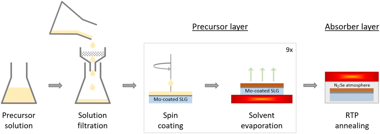 | ||
| Fig. 1 Schematic of the precursor layer fabrication. Reproduced and adapted with permission from Elsevier from ref. 10 under the terms of Creative Commons Attribution License (CC BY), copyright 2023. | ||
X-ray fluorescence (XRF) was used to determine metal ratios using a 45 keV X-ray source (Oxford Instruments, XTF-5011) and a Si p–i–n detector (Amptek, XR-100CR). The peak areas of the Kα lines of Cu, Zn and Sn were used and were compared to a reference samples, which was measured by ICP-MS. Thermogravimetric analysis (TGA) was performed on ∼33 mg of solution in an aluminum crucible using a thermal analyzer (NETZSCH STA 449 F3 Jupiter). The sample was heated to 550 °C at a heat rate of 5 °C min−1 under constant nitrogen purge of 30 ml min−1. The onset temperature of the mass loss was determined at the intersection point of the initial mass baseline and the tangent to the TGA curve at the point of its steepest gradient. X-ray diffraction (XRD) patterns were recorded using a Bruker D8 diffractometer with Cu Kα radiation at a wavelength of 1.5418 Å, beam voltage of 40 kV and beam current of 40 mA. 2θ/θ scans were performed with a step size of 0.02°, a scan rate of 0.1 s per step, and an incident beam size of ∼1 cm for the precursor layer and 2 mm for the absorber layer. High-resolution scans of the absorbers in the 2θ ranges 11–18° and 28–34° were measured using a scan rate of 1.0 s per step. Optical microscope images were recorded using a LEICA EZ4 HD microscope. Scanning electron microscopy with energy-dispersive X-ray spectroscopy (SEM-EDX) experiments were performed on a dual beam FIB-SEM Helios 660 (Thermo Fischer Scientific). 15 kV accelerating voltage and 0.1 nA of beam current were used for both imaging and EDX mapping. J–V curves were recorded under 100 mW cm−2, 22 °C setting temperature and (AM1.5G solar spectrum) using a solar simulator. The solar simulator was calibrated with a certified Si diode. To record external quantum efficiency (EQE) spectra, a chopped white light source (900 W halogen lamp) with a LOT MSH-300 monochromator was used.
3 Results and discussion
Henceforth, samples fabricated from pure chloride solutions will be referred to as Cl-only, samples fabricated from acetate-chloride precursor solutions will be referred to as OAc–Cl, and samples fabricated from nitrate-chloride precursor solutions will be referred to as NO3–Cl.3.1 Results
XRF measurements were performed on precursor and absorber layers to determine metal ratios. Fig. 2 shows the Cu/Sn ratios of the precursor and absorber layer with respect to the Cu/Sn ratio in the solution. The manufacturing steps are illustrated in Fig. 1. The Cu/Sn ratio of the solution was calculated from the concentration of CuCl2 and SnCl2 in the solution. The accuracy of this calculation was verified by ICP-MS measurements of a solution, which was performed by a private company. The target Cu/Sn ratio of the solution (1.12) is in good agreement with the measured Cu/Sn ratio by ICP-MS at 1.10 (ESI, Table S1†). The grey dashed line in Fig. 2 represents the region of no change in Cu/Sn between solution, and precursor and absorber, respectively. It will be referred to as iso-Cu/Sn. The Cu/Sn ratios for the Cl-only precursor samples are found above the dashed line indicating a larger Cu/Sn ratio in the precursor compared to the solution. NO3–Cl samples are also found slightly above the iso-Cu/Sn line, but the deviation is less pronounced than for Cl-only. OAc–Cl samples, on the other hand, are found mostly on the iso-Cu/Sn line. Importantly, deviations from the iso-Cu/Sn line do not depend on the nominal Cu/Sn ratio, but are instead influenced by the type of precursor solution. Therefore, the ranges of nominal Cu/Sn ratio were chosen based on the target composition range for the resulting absorber layer, which determines the device efficiency. | ||
| Fig. 2 Cu/Sn ratio of the precursor layer (hollow markers) and the absorber layer (solid markers) are shown with respect to the Cu/Sn ratio in the solution. Cl-only samples are drawn as orange square markers, OAc–Cl samples are drawn as blue circle markers and NO3–Cl samples are drawn as green diamond markers. The grey dashed line marks identical Cu/Sn ratios between solution and precursor or absorber (iso-Cu/Sn line). | ||
The additional increase in Cu/Sn ratio between the precursor and absorber layer seen in Fig. 2 has been reported before, and has been assigned to evaporation of SnS(e)2−x phases during annealing.20–22 Here, the deviation of Cu/Sn ratio between precursor and absorber is mostly unchanged for the different solution formulations and is hence not part of our study. In the following, we focus on the Cu/Sn ratio variation between solution and precursor.
The origin for Cu/Sn ratio change can occur during filtration, spin coating or solvent evaporation. To pinpoint the occurrence of the deviation, three precursor layers were fabricated from a Cl-only solution with nominal Cu/Sn ratio of 1.15 (Table 1). The first precursor layer was fabricated with the exact same procedure as shown in Fig. 1, for the second sample, the filtration step was omitted and the third sample was fabricated with lower solvent evaporation temperature (250 °C instead of 320 °C). The Cu/Sn ratios of the precursor layers were determined by XRF. While the Cu/Sn ratio of the reference precursor layer was found at 1.44 ± 0.04, the layer with omitted filtration step showed 1.40 ± 0.07, and the layer with lower temperature 1.38 ± 0.04.
| Solution Cu/Sn | Precursor layer Cu/Sn | |
|---|---|---|
| Reference | 1.15 | 1.44 ± 0.04 |
| w/o Filtration | 1.15 | 1.40 ± 0.07 |
| Reduced temperature (250 °C) | 1.15 | 1.38 ± 0.04 |
Due to the apparent influence of temperature on the Cu/Sn ratio, and the risk of incomplete solvent evaporation upon further reduction of temperature given the boiling point of DMSO at 189 °C,23 thermogravimetric analysis was performed. Fig. 3 shows the TGA profiles of the Cl-only and the OAc–Cl solution with the former acting as model solution for Cu/Sn variation and the latter for no Cu/Sn variation, respectively. The blue shaded area represents the relative weight of DMSO + H2O, with the latter originating from hydrated precursor chemicals. The yellow shaded area highlights the sum of Cu, Zn, Sn and Li (Me) plus the sulfur content from thiourea (STu), and the green shaded area represents the remaining organic residuals. The different metal salt concentrations and precursor molecular weights in the two recipes are responsible for the different heights of the shaded areas. The TGA profile of the Cl-only solution reveals four dominant mass loss steps at onset temperatures of 100 °C, 222 °C, 256 °C and 430 °C, respectively. The OAc–Cl solution, on the other hand, has a TGA profile with three mass loss steps at onset temperatures of 101 °C, 277 °C and 432 °C, respectively.
 | ||
| Fig. 3 TGA of the Cl-only (a) and the OAc–Cl (b) precursor solution are shown. The background colors indicate the total mass of the corresponding components, with blue corresponding to solvents, green to organic residuals and yellow to the remaining metals and sulfur originating from thiourea. The dashed transparent line indicates the mass loss rate. (c) XRD patterns of the precursor layers fabricated from the solutions in (a) and (b). (d) TGA measurement of 0.49 M SnCl4 in DMSO. The black dashed line indicates the mass of Sn(DMSO)2Cl4 complex assuming that each Sn(IV) is coordinated. | ||
Clark et al. have recently reported thermogravimetric analysis of a solution containing chloride and acetate salts,24 with similar TGA profile as the OAc–Cl solution here. The first step was assigned to DMSO and H2O evaporation, the second step was explained by decomposition and volatilization of thiourea (Tu) and other organic compounds and the third step indicates the decomposition reaction of CZTS.20,24,25 At about 320 °C, the TGA of Cl-only reaches the total mass of Me + STu, while OAc–Cl is still above this mass level at the same temperature. The negative slope of the curve at this temperature indicates ongoing decomposition of CZTS.
Fig. 3c shows XRD patterns of a Cl-only precursor and OAc–Cl precursor. The Cu/Sn ratios of the precursor layers are 1.58 and 1.57, respectively. The positions of the reflections in the diffractograms are identical for both samples. The peaks at ∼28.4, ∼47.3 and ∼56.2° are assigned to CZTS,26 and the peaks at ∼40.5, ∼58.6 and ∼73.7° are assigned to Mo from the back contact.27 Additional peaks with unknown origin are observed at ∼36.5, and ∼38.7°.
A simplified solution system of 0.49 M SnCl4 in DMSO was fabricated, which is the same Sn-concentration as in the standard Cl-only precursor solution. The solution was analyzed by TGA and the results are shown in Fig. 3d. Two main mass loss steps were found at onset temperatures 104 °C and 232 °C, respectively. During the first step, ∼83% of the total mass is lost, and the remaining 17% is lost in the second step resulting in ∼0% residual mass.
3.2 Model for Sn loss
An increase in Cu/Sn ratio between solution and precursor layer can either be explained by a gain in Cu, or a loss of Sn. Since the solution is the only Cu source, Sn loss is the likely explanation for increasing Cu/Sn ratio. Cl-only precursor layers show the strongest deviation from the iso-Cu/Sn line out of the investigated solutions, which means that Cl-only results in the most pronounced Sn loss. Substitution of Zn(NO3)2 and Li(NO3) for ZnCl2 and LiCl, respectively, mitigates the Sn loss, as the Cu/Sn ratios of the NO3–Cl precursor layers have a smaller deviation from the iso-Cu/Sn line compared to the Cl-only solution (Fig. 2). Substituting Zn(OAc)2 and Li(OAc) for ZnCl2 and LiCl, on the other hand, results in almost no Sn loss between solution and precursor layer making this the most effective Sn loss mitigation strategy.To identify the mechanism for Sn loss between solution and precursor, the path from Sn-chemical – SnCl2·2H2O – to the precursor layer must be understood. Upon dissolving CuCl2 and SnCl2 in DMSO, a certain amount of Sn2+ gets oxidized to Sn4+, as described in eqn (1).12 Correspondingly, twice as many Cu2+ ions are reduced to Cu+. Remaining Sn2+ ions coordinate with thiourea and Cl− anions to form Sn(Tu)xCl2, as reported by Gong et al. through elemental analysis.16 In contrast, the same authors observed that Sn4+ forms a Sn(DMSO)2Cl4 complex when only Cl− anions are present. They also reported that the use of Zn(OAc)2 instead of ZnCl2 prevents the formation of this complex due to reduced Cl− concentration in the solution. However, the exact mechanism remained unclear.16,28
We thus hypothesize that the Sn(IV)-complex composition depends on the availability of ligands, so that Sn(DMSO)2Cl4 can be written as Sn(DMSO)2X4, with X standing for potential ligands. In Cl-only solutions, Cl− is the only available ligand, so that X = Cl. However, upon partial substitution of chloride precursor chemicals by acetate (or nitrate) precursor chemicals, the more general term Sn(DMSO)2X4 should be used. That is, Sn4+ is a hard Lewis acid, and Cl− and OAc− (and also NO3−) are hard Lewis bases. Coordination of Sn4+ by OAc− (or NO3−) instead of Cl− is thus possible, and we do not see any reason that preferential coordination with either ligand would occur, according to HSAB theory. Hence, a complex with mixed ligands should be considered, which, in the case of the OAc–Cl solution, would be Sn(DMSO)xCly(OAc)4−y.
Next, the properties of Sn(DMSO)2Cl4 in Cl-only solutions are investigated. The Sn(DMSO)2Cl4 complex has low solubility in DMSO,16,28 and could therefore precipitate. This could explain the variation in Cu/Sn ratio, if the filtration step is skipped (Table 1), as filtration possibly removes those precipitates from the solution. However, considering the standard deviations in Table 1, the difference in Cu/Sn ratio upon filtration is minor, meaning that it cannot be the main mechanism for Sn loss. Additional ICP-MS measurements performed on a Cl-only solution before and after filtration confirm that Sn loss due to filtration is not significant (ESI, Table S1†).
Besides low solubility, the Sn(DMSO)2Cl4 complex decomposes at elevated temperatures, which results in formation of volatile SnCl4.16 Comparison of the TGA profile of the OAc–Cl solution with the profile of the Cl-only solution reveals many similarities regarding shape and onset temperatures. Consequently, the mass loss steps are believed to be identical: DMSO and H2O evaporation, decomposition and volatilization of thiourea and other organic compounds and decomposition reaction of CZTS. It should be noted that DMSO and H2O evaporation cannot explain the first mass loss step in OAc–Cl alone. It is possible that other residuals already evaporate below 200 °C.24
However, there are two main differences in the TGA curves. On the one hand, the Cl-only solution shows an additional mass loss step at an onset temperature of 222 °C, which is neither seen in the OAc–Cl solution (Fig. 3) nor in the profile reported by Clark et al.24 On the other hand, the mass levels of the two solutions at 320 °C, which is the temperature for solvent evaporation after spin coating, are different. The TGA of the OAc–Cl solution suggests some remaining organic residuals, because the curve has not yet reached the mass of Me + STu. The Cl-only solution, on the other hand, reaches this level at ∼320 °C. One explanation could be that there are less organic residuals remaining. The other explanation is based on the additional loss mechanism in the Cl-only solution, which is absent in the OAc–Cl solution. Interestingly, the discrepancy at 320 °C is about as large as the mass loss during the additional step.
We hypothesize a Sn loss mechanism in the Cl-only solution occurring at an onset temperature of 222 °C via decomposition of the Sn(DMSO)2Cl4 complex. Sn(DMSO)2Cl4 decomposition has been previously reported to occur at 177 °C in DMSO-containing water (20%),29 which is clearly lower than the onset temperature we observed, possibly due to different solvent systems. Given that the decomposition product, SnCl4, has a boiling point of 114 °C,30 it would immediately evaporate after complex decomposition. This mechanism could explain Sn loss. It also aligns well with the results reported in Table 1, which suggest that the temperature rather than the filtration is responsible for Sn loss. A Sn loss mechanism at 222 °C would also explain why the reduction of solvent evaporation temperature to 250 °C showed signs of mitigation, but was not enough to stop Sn loss completely.
The simplified solution system was fabricated to support this hypothesis (Fig. 3d). The first mass loss step is assigned to DMSO evaporation. The second mass loss step, which has a very similar onset temperature as found in Fig. 3a, can only be explained by a Sn compound loss, given that the residual mass drops to ∼0% after this step. The expected weight of a Sn(DMSO)2Cl4 complex, assuming that every Sn in the solution is coordinated by four Cl and two DMSO ligands, is 16.7%, which aligns well with the mass loss in the second step. Consequently, the second step is assigned to the decomposition process of Sn(DMSO)2Cl4, followed by immediate evaporation of all decomposition products. The decomposition temperature of the Sn(DMSO)2Cl4 complex in a pure DMSO solution is hence found at 232 °C, in contrast to the value reported in literature in DMSO-containing H2O.29 The apparent deviation in onset temperature of the decomposition process of the complex in the Cl-only solution and the simplified solution (222 °C vs. 232 °C) could be explained by matrix effects.
To further support the hypothesis of Sn loss at 222 °C, TGA-MS of the Cl-only and the OAc–Cl solutions were performed (ESI, Fig. S1†). We observed signals at atomic mass 35 and 37 in the relevant temperature range in the Cl-only solution, which are absent in the OAc–Cl solution. The ∼3![[thin space (1/6-em)]](https://www.rsc.org/images/entities/char_2009.gif) :1 ratio between the two fragments point to the isotopes 35Cl (relative abundance: 75.8%) and 37Cl (relative abundance: 24.2%).31 The detection of Cl during this step supports the hypothesis of Sn(DMSO)2Cl4 complex decomposition and subsequent SnCl4 evaporation in the Cl-only solution. We further looked for signals at masses corresponding to Sn, SnCl, SnCl2, SnCl3 or SnCl4, but observed none of those. The absence of such fragments could be assigned to matrix effects such as ion suppression, which decrease the concentration of the Sn fragment to values below the detection limit of the machine.32
:1 ratio between the two fragments point to the isotopes 35Cl (relative abundance: 75.8%) and 37Cl (relative abundance: 24.2%).31 The detection of Cl during this step supports the hypothesis of Sn(DMSO)2Cl4 complex decomposition and subsequent SnCl4 evaporation in the Cl-only solution. We further looked for signals at masses corresponding to Sn, SnCl, SnCl2, SnCl3 or SnCl4, but observed none of those. The absence of such fragments could be assigned to matrix effects such as ion suppression, which decrease the concentration of the Sn fragment to values below the detection limit of the machine.32
Sn(DMSO)2Cl4 complex decomposition and subsequent SnCl4 evaporation is the most likely Sn loss mechanism in Cl-only solution. The situation in the OAc–Cl solution, on the other hand, is different. Given the availability of OAc− besides Cl−, the complex Sn(DMSO)xCly(OAc)4−y is expected. The thermal stability of this complex compared to Sn(DMSO)2Cl4 is unknown. However, we assume that the melting points of the stannous salts are a rough indication of the stability of the Sn(DMSO)xCly(OAc)4−y complexes. The melting points of SnCl4, SnCl2(OAc)2 and Sn(OAc)4 are −32 °C,33 213 °C (with decomposition),34 and 241 °C,35 respectively. This would suggest that coordination of acetate ligands stabilizes the complex and it might explain the mitigated Sn loss in the OAc–Cl solution. The comparison can be extended to the NO3–Cl solution: Sn(NO3)4 has a melting point of 91 °C,36 which would suggest a complex with a stability larger than Sn(DMSO)2Cl4 but lower than Sn(DMSO)2(OAc)4. In fact, Fig. 2 suggests that NO3–Cl mitigates Sn loss compared to Cl-only, but still shows more Sn loss than OAc–Cl, which would align well with the predicted stability based on the melting points of the stannous salts.
It should be noted that the metal salt concentrations of the solution systems Cl-only and OAc–Cl (and NO3–Cl), are different. Different metal concentrations were chosen, because using the same concentrations for the OAc–Cl solution and for the Cl-only solution resulted in significantly thinner absorber layers for the former. To avoid a potential effect of absorber thickness on device performance later, the thickness of the OAc–Cl (and NO3–Cl) absorbers was increased by raising the metal salt concentrations in the OAc–Cl (and NO3–Cl) solutions up to the solubility limit. Alternative depiction of the results from Fig. 2 in Fig. S2 (ESI)† do not show any trend for the Cu/Sn ratio with respect to the metal salt concentration or the thiourea concentration on Sn loss.
The mechanism for Sn loss proposed herein, would suggest complete Sn(IV) loss, so that the Cl-only solution eventually only contains Sn2+. Surprisingly, this is not the case. That is, the Cu/Sn ratio in the precursor can be estimated using the Cu/Sn ratio from Table 1 and eqn (1). The detailed calculations are found in ESI.† Under the assumption that Sn(IV) were lost completely, the Cu/Sn ratio in the precursor layer of the reference sample in Table 1 (Cl-only) would be 2.67. However, measurements report a significantly smaller value of 1.44 (Table 1). A possible explanation would be incomplete reaction of eqn (1), which would leave a larger concentration of Sn2+ behind. On the one hand, this would also result in Cu(II)-complexes in the solution, which would tint the solution blue due to d–d transitions, which was not observed. On the other hand, while it has been reported in literature, that the kesterite phase can form from Sn(II), the formation mechanism in that case involves several secondary phases in the precursor layer.16 These phases would then be turned into CZTSSe during annealing. In contrast, kesterite formation via Sn(IV) occurs via CZTS phase with low crystallinity in the precursor.16 Our results clearly suggest the presence of CZTS phase with low crystallinity (Fig. 3c), so called amorphous CZTS,16 or a-CZTS, and the reproducibility of this measurement was confirmed by additional measurements of identical absorbers shown in Fig. S3 (ESI).† Although there are a few unidentified reflections in the XRD (36.5 and 38.7°) besides the a-CZTS peak in the precursor film, their peak positions do not align with the phases expected from the Sn(II) formation route such as ZnS, SnS and Cu2−xS.16,17 Additional Raman measurements (ESI Fig. S3†) did also not reveal signals linked to such secondary phases. In addition, the intensity of the unknown phases in Fig. 3c is low compared to a-CZTS. Consequently, kesterite formation via Sn(II) is probably negligible and the Sn(IV) formation route is expected to be the dominant CZTSSe formation path in our system. This conclusion also dismisses the hypothesis of an incomplete reaction of eqn (1), which would require kesterite formation via Sn(II).
Instead, we propose the presence of another, unidentified Sn(IV)-complex besides Sn(DMSO)2X4, which remains in the precursor layer after solvent evaporation. This would explain, why Sn(IV) is only partly lost during Cl-only precursor fabrication.
3.3 Consequences of Sn loss
As it can be seen in Fig. 2, targeting an absorber Cu/Sn ratio using a Cl-only solution requires Sn excess in the solution to accommodate for Sn loss. To investigate the effect of different Cu/Sn ratios in the solution on absorbers, four solutions were made, with low and high Cu/Sn ratio for both, Cl-only and OAc–Cl, respectively. From these solutions, absorbers were fabricated and characterized by XRD. Fig. 4a shows diffraction patterns for absorbers fabricated from Cl-only solutions, and Fig. 4b shows diffraction patterns for absorbers fabricated from OAc–Cl solutions. The numbers in brackets in Fig. 4 stand for the Cu/Sn ratio of the solution. The Cl-only absorber fabricated from a solution with a Cu/Sn ratio of 1.15 was measured twice on different spots. Only the ranges 11–18° and 28–34° are shown, with full range scans shown in Fig. S4 (ESI)† for selected samples. The peaks at ∼15.7, ∼17.5 and ∼28.4° are assigned to CZTSSe,37 and are found in all patterns. The broad peak at ∼31.9° is assigned to MoSe2,38 and is present in all patterns. The patterns corresponding to low Cu/Sn ratio in the solution show additional peaks at ∼14.4, ∼29.1 and ∼30.8°. An additional absorber fabricated from a Cl-only solution with low Cu/Sn ratio was analyzed by XRD and shows a similar pattern (ESI, Fig. S5†). | ||
| Fig. 4 (a) XRD patterns for Cl-only absorber layers fabricated from solutions with various Cu/Sn ratio (number in brackets). Two measurement spots on the absorber fabricated from a solution with Cu/Sn ratio of 1.15 are shown. (b) XRD patterns for OAc–Cl absorber layers fabricated from solutions with various Cu/Sn ratio (number in brackets). | ||
The additional reflections in absorbers fabricated from low Cu/Sn solutions in Fig. 4 are assigned to SnSe2.39 Interestingly, the SnSe2 secondary phases accumulate in certain areas, so that they are not found on the whole absorber, as confirmed by the different measuring spots on the Cl-only (1.15) absorber. Low Cu/Sn ratios in the solution result in residual Sn2+ due to an incomplete reaction (eqn (1)). Part of this remaining Sn(II) could be oxidized to Sn(IV) with a different mechanism. One such mechanism involving DMSO has been proposed using iodine salts.40,41 Yet, this particular reaction would form SnO2 as a byproduct, which could not be evidenced by XRD, neither in the precursor nor in the absorber layer (Fig. 3c and 4). Remaining Sn(II), will, in contrast to Sn(IV), coordinate with Tu to form Sn(Tu)xCl2, which will decompose to SnS at elevated temperatures.16,42 The concentration of Sn2+, and later SnS, is too low to be identified by e.g., XRD in the precursor layer (Fig. 3c). Yet, once SnS turns into SnSe2 in chalcogen atmosphere with sufficient partial pressure, it becomes visible in XRD.17,20 Therefore, excessive presence of Sn2+ in the precursor solution will eventually result in SnSe2 formation in the absorber layer, which explains the presence of SnSe2 peaks in the XRD patterns for low nominal Cu/Sn ratios.
This mechanism becomes relevant when using a solution subject to Sn loss (e.g., Cl-only). While the occurrence of secondary phases is not directly explained by the choice of the solution system, it is an indirect consequence. Using a Cl-only solution for absorber fabrication results in Sn loss as discussed in the previous section. Sn loss occurs via the Sn(DMSO)2Cl4 complex, meaning that Sn is lost as Sn(IV). Accommodating for this Sn loss by fabricating Sn-rich solutions is only a partial solution. The Sn concentration in the absorber can indeed be tuned thereby. However, doing so increases concentration of Sn2+ instead of Sn4+, due to the stoichiometry of eqn (1), causing SnSe2 formation. Consequently, the Cu/Sn ratio in the precursor solution of a Cu2+–Sn2+ system determines the appearance of SnSe2 secondary phases in the absorber.
Finally, it is noted that the area under the peak assigned to MoSe2 decreases for decreasing Cu/Sn ratio. As demonstrated before, lower Cu/Sn ratio eventually results in the formation of SnSe2 phases in the absorber. It is possible that the Se consumption for this reaction reduces the availability of Se to form MoSe2, so that the amount of MoSe2 is lower when using lower nominal Cu/Sn ratio.
3.4 Solar cells
Solar cells are fabricated from the four absorbers used in the previous section, to investigate the influence of Sn loss on the PV performance. XRF measurements were performed on the respective precursors and absorbers and the results are reported in Table 2. The observed appearance of SnSe2 by XRD is summarized in a separate column. The last column additionally shows the average power conversion efficiency. The Cl-only samples show a significant Sn loss between solution and precursor, in accordance with previous results. The best PV performance is reached for absorbers with Cu/Sn ratio of 1.68 (Cu/Sn solution ratio 1.15 for Cl-only and 1.58 for OAc–Cl), while both lower and higher Cu/Sn ratios in the absorber result in very low efficiencies. The standard deviation of the cells fabricated from Cl-only (1.15) is higher than for the other samples.| Cu/Sn solution | Cu/Sn precursor | Cu/Sn absorber | Presence of SnSe2 in absorber (XRD) | PCE (%) | |
|---|---|---|---|---|---|
| Cl-only (1.15) | 1.15 | 1.58 | 1.68 | Yes | 9.6 ± 1.1 |
| Cl-only (1.56) | 1.56 | 1.96 | 2.16 | No | 0.2 ± 0.1 |
| OAc–Cl (1.14) | 1.14 | (no data) | 1.26 | Yes | 1.3 ± 0.2 |
| OAc–Cl (1.58) | 1.58 | 1.56 | 1.68 | No | 9.1 ± 0.2 |
The results in Table 2 confirm the need for favorable Cu/Sn ratio in the absorber as only absorbers with a Cu/Sn ratio of 1.68 achieve an average power conversion efficiency >9%. The other absorbers result in very poor PV performance. Therefore, to properly compare the PV performance originating from the different solutions, the conditions Cl-only (1.15) and OAc–Cl (1.58) were used, and more absorbers were fabricated targeting an absorber Cu/Sn ratio in the range 1.65–1.75. This is, because samples with Cu/Sn < 1.65 often feature SnSe2 secondary phases, which could mask the influence originating from the anion selection.43 Sn-poor absorbers (Cu/Sn > 1.75) usually do not contain SnSe2, but at the cost of low PV performance (Fig. 4 and Table 2). To fabricate absorbers with corresponding Cu/Sn ratios, the ratios in Table 2 were targeted, which means that Cl-only solutions were Sn-rich.
Fig. 5a and b depict JV curves of devices fabricated from Cl-only solutions and OAc–Cl solutions, respectively. The devices do not have an anti-reflective coating. For each sample, the best and worst JV curves are shown as dashed and solid lines, respectively. The deviation between best and worst JV curve is larger for the Cl-only than for the OAc–Cl devices. Fig. 5c–f show VOC, short circuit current density (JSC), fill factor (FF) and power conversion efficiency (PCE) for each cell, plotted vs. the difference in Sn concentration between solution and absorber, since the Sn loss between precursor and absorber is similar for all solution systems (Fig. 2). The efficiency of Cl-only devices is higher than OAc–Cl devices, which seems to arise mainly from the higher JSC in the Cl-only devices. Despite the better performance of Cl-only devices, Fig. 5 further reveals that devices without, or only minor, Sn loss (OAc–Cl) show a narrower distribution of VOC, FF and PCE within the same sample. Most Cl-only devices, on the other hand, contain at least one cell, which performs significantly worse than the average performance on the same sample.
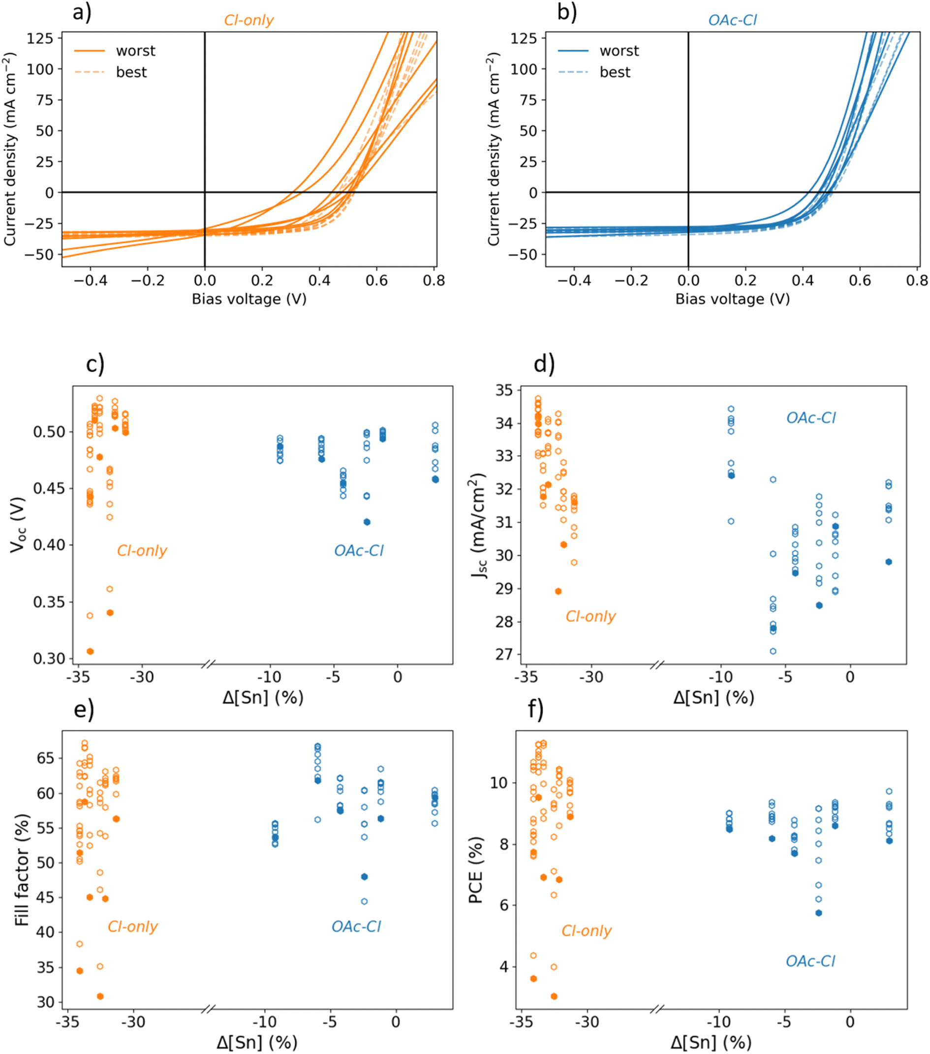 | ||
| Fig. 5 JV performance of Cl-only (orange) and OAc–Cl (blue) solar cells. In (a) and (b), JV curves of the best (transparent, dashed) and the worst (opaque, solid) cell for each sample are shown. The distribution of VOC, JSC, fill factor and power conversion efficiency with respect to the Sn loss between solution and absorber are shown in (c)–(f), respectively. For each sample, the worst cell is marked in subfigures (c)–(f) as a filled data point. The uniformity of the PV performance is improved in OAc–Cl devices compared to Cl-only devices. | ||
To visualize the influence of Sn loss on performance, Fig. 5c–f shows performance metrics (VOC, JSC, FF, PCE) against Sn loss. It is observed that the performance level of Cl-only samples tends to be higher than for the OAc–Cl samples. This also results in the best device of this series being fabricated with a Cl-only solution. After deposition of an anti-reflective coating on this particular device a power conversion efficiency of 11.8% (12.5% active area) was reached (Fig. S6 in the ESI†). The higher performance level of Cl-only stems from higher JSC values compared to OAc–Cl.
The JSC loss for OAc–Cl samples is related to long-wavelength photons (see EQE spectra in ESI, Fig. S7†). SEM cross-section images (ESI, Fig. S8†) show that the OAc–Cl absorbers are considerably thinner (1.21 ± 0.11 μm) than the Cl-only absorbers (2.35 ± 0.19 μm), despite higher metal salt concentration in the solution. The variation in thickness may arise from changes in solution properties that influence the spin coating process, such as alterations in the viscosity of the precursor solution.44 Since absorber thickness can affect morphology,45 the observed differences – such as smaller grains and the absence of a double layer in the OAc–Cl sample – could be attributed to this thickness variation. The thinner OAc–Cl absorber layer could result in decreased absorption of long-wavelength photons, which would reflect in lower JSC. However, the absorption coefficient of kesterite is high (>104 cm−1),46 so that the penetration depth of long-wavelength photons is rather shallow. Therefore, the JSC loss could instead be explained by a collection problem, given the commonly short minority carrier lifetime and corresponding short diffusion length in kesterite absorbers,47 or by more detrimental rear-interface recombination in the thinner OAc–Cl absorbers. Yet, it should be noted that the Cl-only fabrication process has been optimized for years in our laboratory. The OAc–Cl route, on the other hand, has only been introduced in our laboratory recently, and it could be that certain parameters will improve with fine-tuning of the process.
Most Cl-only samples shown in Fig. 5 contain at least one clearly underperforming cell. The PCE of those cells is mainly affected by FF, but also by VOC to some extent. It can be seen in Fig. 5a (and ESI, Fig. S9†) that the fill factor loss mainly originates from low parallel resistance (Rp) and high diode ideality factor (n). Some cells additionally show an increase in series resistance (Rs).
A possible explanation for low Rp and high n for the Cl-only samples is the occurrence of SnSe2 secondary phases. It was shown before that the Cl-only solution resulting in favorable Cu/Sn ratio in the absorber results in SnSe2 formation (Fig. 4). To investigate further, optical and electron microscopy was employed. Fig. 6a shows a top-view image of a Cl-only device recorded by an optical microscope. Under grazing incidence illumination, small dots become visible due to light reflection. An SEM top-view image of such a small dot reveals disk-shaped secondary phases in the micrometer range, which explains the visibility of the impurities by naked eye (Fig. 6b). EDX measurements indicated that these secondary phases are rich in Sn and Se. The secondary phase found in Fig. 6 is thus assigned to SnSe2, in accordance with previous results.17,48 Fig. S10 in the ESI† shows additional top-view SEM images of the same absorber revealing more SnSe2 phases. Interestingly, the SnSe2 phases in the Cl-only absorber are not homogeneously distributed, but are concentrated, here, on the two cells at the top of Fig. 6a. This supports the observation from XRD in Fig. 4a, where secondary phases were found only on certain areas of the absorber.
 | ||
| Fig. 6 (a) Top-view optical microscopy image Cl-only sample showing several cells. The bright dots towards the top of the image are identified by top-view SEM image of a Cl-only absorber (b) with corresponding EDX maps. | ||
Temgoua et al. demonstrated that high surface density of SnSe2 is detrimental for Rp.48 Furthermore, Gong et al. reported high diode ideality factors (>2) for SnSe2-containing devices. They explained this observation by a high concentration of defects near the absorber surface, which causes severe Shockley-Read-Hall recombination.17 This manifests in an increased J0, which is also observed here. Worst cells shown in Fig. 5a exhibit J0 values, which are at least one order of magnitude higher than the J0 of the best cells of the respective sample (data not shown). The non-uniform distribution of SnSe2 in Cl-only devices then results in Rp and n degradation only for some cells on the sample, which causes the non-uniform PV performance.
Therefore, the choice of the anion can be linked to the uniformity of the PV performance. However, we want to emphasize that the choice of the anion is not directly responsible for non-uniformity. It is a consequence of Sn loss compensation by Sn-rich solutions, which suggests that only by making a Cu2+–Sn2+ solution resistant to Sn loss, an acceptable Cu/Sn ratio without secondary phases can be achieved in the absorber. And only the absence of secondary phases such as SnSe2 enables the uniformity of the device.
Finally, it should be noted that the aim to fabricate Cu-poor and Zn-rich absorbers driven by material quality considerations is a general disadvantage of the Cu2+–Sn2+ precursor system, compared to the Cu+–Sn4+ one. Although Cu-poor conditions result in better PV performance,49,50 they also result in off-stoichiometry of eqn (1), even if a Sn-loss-free solution such as OAc–Cl is used. As demonstrated in this work, Cu-poor, hence Sn-rich, solutions yield residual Sn2+, which can be turned into SnSe2. The extent of SnSe2 in OAc–Cl may only be minor and was not detected by any method in our work, but it might still negatively affect the performance level of absorbers fabricated from a Cu2+–Sn2+ precursor system. Given that the Cu/Sn ratio in the solution of the Cu2+–Sn2+ system should be 2, and <2 in the absorber, mitigating Sn loss might not be enough. In fact, hypothetical Cu loss could be desirable in the Cu2+–Sn2+ system. Alternatively, another strategy to oxidize Sn2+ could also be an approach to circumvent this potential limitation.
4 Conclusion
In this work, we investigated the Cu2+–Sn2+ precursor system for solution-processed CZTSSe absorber fabrication, with the goal to address Sn loss during processing. We compared solutions fabricated from metal salts with different anions and found that high abundance of Cl− anions in the solution results in Sn(IV) loss during high temperature solvent evaporation via the decomposition of the Sn(DMSO)2Cl4 complex into volatile products. The common strategy to accommodate for Sn(IV) loss by fabricating Sn-rich precursor solutions is not optimal, as it results in excess Sn2+, and ultimately in undesired SnSe2 secondary phase formation in the absorber. Local shunt paths are formed leading to non-uniform PV performance. We demonstrated that partial substitution of acetate salts for chloride salts mitigates Sn(IV) loss, as it avoids the formation of the problematic Sn(IV)-complex. The resulting CZTSSe devices do not show SnSe2 secondary phases, and have thus higher uniformity and higher reproducibility, which is a crucial aspect in view of module fabrication. Further adjustment on the absorber layer thickness of the acetate-chloride recipe is required to achieve higher power conversion efficiency.Data availability
Data for this article are available at https://zenodo.org/communities/custom-art/ under DOI https://doi.org/10.5281/zenodo.11369961 (once the manuscript has been accepted).Author contributions
S. Moser: conceptualization, methodology, validation, investigation, data curation, writing – original draft, writing – review and editing, visualization. J. Krummenacher: methodology, validation, investigation, data curation, writing – review and editing. A. Aribia: methodology, validation, writing – review and editing. J. Morzy: methodology, validation, investigation, data curation, writing – review and editing. R. Carron: conceptualization, methodology, writing – review and editing, supervision, project administration, funding acquisition.Conflicts of interest
There are no conflicts of interest to declare.Acknowledgements
This project has received funding from the European Union's Horizon 2020 research and innovation program under grant agreement no 952982 (Custom-Art). PD Dr Arndt Remhof from the Materials for Energy Conversion Laboratory at Empa is gratefully acknowledged for assistance regarding Thermogravimetric analysis. The Materials for Energy Conversion Laboratory is further acknowledged for granting access to TGA measurement facilities. Rico Muff from the Transport at Nanoscale Interfaces Laboratory at Empa is gratefully acknowledged for carrying out Raman measurements. The Transport at Nanoscale Interfaces Laboratory is further acknowledged for granting access to SEM and Raman measurement facilities. The Laboratory for Surface Science & Coating Technologies at Empa is gratefully acknowledged for granting access to XRD measurement facilities.References
- M. He, C. Yan, J. Li, M. P. Suryawanshi, J. Kim, M. A. Green and X. Hao, Kesterite Solar Cells: Insights into Current Strategies and Challenges, Adv. Sci., 2021, 8, 2004313, DOI:10.1002/advs.202004313.
- A. Wang, M. He, M. A. Green, K. Sun and X. Hao, A Critical Review on the Progress of Kesterite Solar Cells: Current Strategies and Insights, Adv. Energy Mater., 2022, 13, 2203046, DOI:10.1002/aenm.202203046.
- M. A. Green, E. D. Dunlop, M. Yoshita, N. Kopidakis, K. Bothe, G. Siefer, D. Hinken, M. Rauer, J. Hohl-Ebinger and X. Hao, Solar cell efficiency tables (Version 64), Prog. Photovolt. Res. Appl., 2024, 32(7) DOI:10.1002/pip.3831.
- S. Hegedus, Thin Film Solar Modules: The Low Cost, High Throughput and Versatile Alternative to Si Wafers, Prog. Photovoltaics Res. Appl., 2006, 14, 393–411, DOI:10.1002/pip.1160.
- T. K. Todorov, K. B. Reuter and D. B. Mitzi, High-Efficiency Solar Cell with Earth-Abundant Liquid-Processed Absorber, Adv. Mater., 2010, 22, E156–E159, DOI:10.1002/adma.201090073.
- T. Todorov, H. W. Hillhouse, S. Aazou, Z. Sekkat, O. Vigil-Galán, S. D. Deshmukh, R. Agrawal, S. Bourdais, M. Valdés, P. Arnou, D. B. Mitzi and P. J. Dale, Solution-based synthesis of kesterite thin film semiconductors, JPhys Energy, 2020, 2, 012003, DOI:10.1088/2515-7655/ab3a81.
- L. Wang, Y. Wang, Z. Zhou, W. Zhou, D. Kou, Y. Meng, Y. Qi, S. Yuan, L. Han and S. Wu, Progress and prospectives of solution-processed kesterite absorbers for photovoltaic applications, Nanoscale, 2023, 15, 8900–8924, 10.1039/d3nr00218g.
- A. Cabas-Vidani, S. G. Haass, C. Andres, R. Caballero, R. Figi, C. Schreiner, J. A. Márquez, C. Hages, T. Unold, D. Bleiner, A. N. Tiwari and Y. E. Romanyuk, High-Efficiency (LixCu1−x)2ZnSn(S,Se)4 Kesterite Solar Cells with Lithium Alloying, Adv. Energy Mater., 2018, 8, 1801191, DOI:10.1002/aenm.201801191.
- S. Moser, A. Aribia, R. Scaffidi, E. Gilshtein, G. Brammertz, B. Vermang, A. N. Tiwari and R. Carron, Controlled Li Alloying by Postsynthesis Electrochemical Treatment of Cu2ZnSn(S, Se)4 Absorbers for Solar Cells, ACS Appl. Energy Mater., 2023, 6, 12515–12525, DOI:10.1021/acsaem.3c02483.
- S. Moser, A. N. Tiwari and R. Carron, Interplay between Li and Na amid co-doped solution-processed Cu 2 ZnSn (S, Se) 4 absorbers for solar cells, Sol. Energy Mater. Sol. Cells, 2023, 250, 112094, DOI:10.1016/j.solmat.2022.112094.
- Y. Gong, Q. Zhu, B. Li, S. Wang, B. Duan, L. Lou, C. Xiang, E. Jedlicka, R. Giridharagopal, Y. Zhou, Q. Dai, W. Yan, S. Chen, Q. Meng and H. Xin, Elemental de-mixing-induced epitaxial kesterite/CdS interface enabling 13%-efficiency kesterite solar cells, Nat. Energy, 2022, 7, 966–977, DOI:10.1038/s41560-022-01132-4.
- H. Xin, J. K. Katahara, I. L. Braly and H. W. Hillhouse, 8% Efficient Cu2ZnSn(S,Se)4 solar cells from redox equilibrated simple precursors in DMSO, Adv. Energy Mater., 2014, 4, 1301823, DOI:10.1002/aenm.201301823.
- J. Zhou, X. Xu, H. Wu, J. Wang, L. Lou, K. Yin, Y. Gong, J. Shi, Y. Luo, D. Li, H. Xin and Q. Meng, Control of the phase evolution of kesterite by tuning of the selenium partial pressure for solar cells with 13.8% certified efficiency, Nat. Energy, 2023, 8, 526–535, DOI:10.1038/s41560-023-01251-6.
- Y. Gong, R. Qiu, C. Niu, J. Fu, E. Jedlicka, R. Giridharagopal, Q. Zhu, Y. Zhou, W. Yan, S. Yu, J. Jiang, S. Wu, D. S. Ginger, W. Huang and H. Xin, Ag Incorporation with Controlled Grain Growth Enables 12.5% Efficient Kesterite Solar Cell with Open Circuit Voltage Reached 64.2% Shockley–Queisser Limit, Adv. Funct. Mater., 2021, 31, 2101927, DOI:10.1002/adfm.202101927.
- Y. Sun, P. Qiu, W. Yu, J. Li, H. Guo, L. Wu, H. Luo, R. Meng, Y. Zhang and S. Liu, N-Type Surface Design for p-Type CZTSSe Thin Film to Attain High Efficiency, Adv. Mater., 2021, 33, 2104330, DOI:10.1002/adma.202104330.
- Y. Gong, Y. Zhang, E. Jedlicka, R. Giridharagopal, J. A. Clark, W. Yan, C. Niu, R. Qiu, J. Jiang, S. Yu, S. Wu, H. W. Hillhouse, D. S. Ginger, W. Huang and H. Xin, Sn4+ precursor enables 12.4% efficient kesterite solar cell from DMSO solution with open circuit voltage deficit below 0.30 V, Sci. China Mater., 2021, 64, 52–60, DOI:10.1007/s40843-020-1408-x.
- Y. Gong, Y. Zhang, Q. Zhu, Y. Zhou, R. Qiu, C. Niu, W. Yan, W. Huang and H. Xin, Identifying the origin of the Voc deficit of kesterite solar cells from the two grain growth mechanisms induced by Sn2+ and Sn4+ precursors in DMSO solution, Energy Environ. Sci., 2021, 14, 2369–2380, 10.1039/d0ee03702h.
- P. Billik and M. Čaplovičová, Synthesis of nanocrystalline SnO2 powder from SnCl4 by mechanochemical processing, Powder Technol., 2009, 191, 235–239, DOI:10.1016/j.powtec.2008.10.017.
- Y. Gong, A. Jimenez-Arguijo, A. G. Medaille, S. Moser, A. Basak, R. Scaffidi, R. Carron, D. Flandre, B. Vermang, S. Giraldo, H. Xin, A. Perez-Rodriguez and E. Saucedo, Li-Doping and Ag-Alloying Interplay Shows the Pathway for Kesterite Solar Cells with Efficiency Over 14, Adv. Funct. Mater., 2024, 2404669, DOI:10.1002/adfm.202404669.
- J. J. Scragg, T. Ericson, T. Kubart, M. Edoff and C. Platzer-Björkman, Chemical Insights into the Instability of Cu2ZnSnS4 Films during Annealing, Chem. Mater., 2011, 23, 4625–4633, DOI:10.1021/cm202379s.
- C. M. Sutter-Fella, A. R. Uhl, Y. E. Romanyuk and A. N. Tiwari, Large-grained Cu2ZnSnS4layerssintered from Sn-rich solution-deposited precursors, Phys. Status Solidi A, 2015, 212, 121–125, DOI:10.1002/pssa.201431147.
- D. Nowak, F. Atlan, D. Pareek, M. Guc, A. Perez-Rodriguez, V. Izquierdo-Roca and L. Gütay, Influence of the precursor composition on the resulting absorber properties and defect concentration in Cu2ZnSnSe4 absorbers, Sol. Energy Mater. Sol. Cells, 2023, 256, 112342, DOI:10.1016/j.solmat.2023.112342.
- H. L. Schläfer and W. Schaffernicht, Dimethylsulfoxyd als Losungsmittel für anorganische Verbindungen, Angew. Chem., 1960, 72, 618–626 CrossRef.
- J. A. Clark, A. R. Uhl, T. R. Martin and H. W. Hillhouse, Evolution of Morphology and Composition during Annealing and Selenization in Solution-Processed Cu2ZnSn(S,Se)4, Chem. Mater., 2017, 29, 9328–9339, DOI:10.1021/acs.chemmater.7b03313.
- J. Madarász, P. Bombicz, M. Okuya and S. Kaneko, Thermal decomposition of thiourea complexes of Cu(I), Zn(II), and Sn(II) chlorides as precursors for the spray pyrolysis deposition of sulfide thin films, Solid State Ionics, 2001, 141(142), 439–446, DOI:10.1016/S0167-2738(01)00740-8.
- A. Ritscher, M. Hoelzel and M. Lerch, The order-disorder transition in Cu2ZnSnS4 - A neutron scattering investigation, J. Solid State Chem., 2016, 238, 68–73, DOI:10.1016/j.jssc.2016.03.013.
- C. Bernuy-Lopez, M. Allix, C. A. Bridges, J. B. Claridge and M. J. Rosseinsky, Sr2MgMoO6-δ: Structure, Phase Stability, and Cation Site Order Control of Reduction, Chem. Mater., 2007, 19, 1035–1043, DOI:10.1021/cm0624116.
- Y. Gong, Y. Zhang, E. Jedlicka, R. Giridharagopal, J. A. Clark, W. Yan, C. Niu, R. Qiu, J. Jiang, S. Yu, S. Wu, H. W. Hillhouse, D. S. Ginger, W. Huang and H. Xin, Erratum to: Sn4+ precursor enables 12.4% efficient kesterite solar cell from DMSO solution with open circuit voltage deficit below 0.30 V, Sci. China Mater., 2021, 64, 52–60 ( Sci. China Mater. , 2021 , 64 , 1304 ) CrossRef CAS.
- M. R. Caira, L. R. Nassimbeni, A. M. Stephen and T. G. Van Schalkwyk, Geometry of the iminium moiety IV Structure of 4,5-dihydro-3,5,5-trimethyl- pyrazolium Aquapentachlorostannate Monohydrate, Acta Crystallogr., Sect. C, 1993, 49, 26–30, DOI:10.1107/S0108270192005146.
- H. Sackmann and A. Boczek, Das Verhalten binärer flüssiger Mischphasen, II1, Z. Phys. Chem., 1961, 29, 329–338 CrossRef CAS.
- M. Berglund and M. E. Wieser, Isotopic compositions of the elements 2009 (IUPAC technical report), Pure Appl. Chem., 2011, 83, 397–410, DOI:10.1351/PAC-REP-10-06-02.
- A. Furey, M. Moriarty, V. Bane, B. Kinsella and M. Lehane, Ion suppression; A critical review on causes, evaluation, prevention and applications, Talanta, 2013, 115, 104–122, DOI:10.1016/j.talanta.2013.03.048.
- J. C. Sheldon and S. Y. J. Tyree, The Donor Properties of POCl3, SeOCl2, CH3COCl, SOCl2 and VOCl3, J. Am. Chem. Soc., 1961, 81, 2290–2296, DOI:10.1021/ja01519a003.
- J. Amaudrut and C. Devin, Préparation de quelques dichlorures dialcanoates d’étain, C. R. Hebd. Seances Acad. Sci. Ser. C Sci. Chim., 1970, 271, 299–302 CAS.
- A. K. Sawyer, C. Frey, R. A. Collupy and R. I. Chase, The action of acetic acid and/or acetic anhydride on either tetraphenyltin or diphenyltin oxide to form tin(IV) acetate, Synth. React. Inorg. Met. Org. Chem., 1989, 19, 969–982, DOI:10.1080/00945718908050648.
- C. C. Addison and W. B. Simpson, Tin(IV) Nitrate: The Relation between Structure and Reactivity of Metal Nitrates, J. Chem. Soc., 1965, 598–602, 10.1039/JR9650000598.
- I. D. Olekseyuk, L. D. Gulay, I. V. Dydchak, L. V. Piskach, O. V. Parasyuk and O. V. Marchuk, Single crystal preparation and crystal structure of the Cu2Zn/Cd,Hg/SnSe4 compounds, J. Alloys Compd., 2002, 340, 141–145, DOI:10.1016/S0925-8388(02)00006-3.
- P. B. James and M. T. Lavik, The crystal structure of MoSe2, Acta Crystallogr., 1963, 16, 1183, DOI:10.1107/s0365110x6300311x.
- K. Liu, H. Liu, J. Wang and L. Feng, Synthesis and characterization of SnSe2 hexagonal nanoflakes, Mater. Lett., 2009, 63, 512–514, DOI:10.1016/j.matlet.2008.10.054.
- M. I. Saidaminov, I. Spanopoulos, J. Abed, W. Ke, J. Wicks, M. G. Kanatzidis and E. H. Sargent, Conventional Solvent Oxidizes Sn(II) in Perovskite Inks, ACS Energy Lett., 2020, 5, 1153–1155, DOI:10.1021/acsenergylett.0c00402.
- J. Pascual, G. Nasti, M. H. Aldamasy, J. A. Smith, M. Flatken, N. Phung, D. Di Girolamo, S. H. Turren-Cruz, M. Li, A. Dallmann, R. Avolio and A. Abate, Origin of Sn(ii) oxidation in tin halide perovskites, Adv. Mater., 2020, 1, 1066–1070, 10.1039/d0ma00245c.
- J. Zhao, F. Wu and X. Han, Impact of Sn4+/Sn2+ ratio in the precursor solution on the performance of CZTSSe solar cell, Mater. Sci. Semicond. Process., 2023, 158, 107359, DOI:10.1016/j.mssp.2023.107359.
- S. G. Haass, C. Andres, R. Figi, C. Schreiner, M. Bürki, Y. E. Romanyuk and A. N. Tiwari, Complex Interplay between Absorber Composition and Alkali Doping in High-Efficiency Kesterite Solar Cells, Adv. Energy Mater., 2018, 8, 1701760, DOI:10.1002/aenm.201701760.
- A. S. H. Makhlouf, 1 – Current and advanced coating technologies for industrial applications, in Woodhead Publishing Series in Metals and Surface Engineering, ed. A. S. H. Makhlouf and I. Tiginyanu, 2011, pp. 3–23, DOI:10.1533/9780857094902.1.3.
- F. Martinho, S. Lopez-Marino, M. Espíndola-Rodríguez, A. Hajijafarassar, F. Stulen, S. Grini, M. Döbeli, M. Gansukh, S. Engberg, E. Stamate, L. Vines, J. Schou, O. Hansen and S. Canulescu, Persistent Double-Layer Formation in Kesterite Solar Cells: A Critical Review, ACS Appl. Mater. Interfaces, 2020, 12, 39405–39424, DOI:10.1021/acsami.0c10068.
- C. Persson, R. Chen, H. Zhao, M. Kumar and D. Huang, Electronic Structure and Optical Properties from First-Principles Modeling, in Copper Zinc Tin Sulfide-Based Thin-Film Solar Cells, 2014, pp. 75–105, DOI:10.1002/9781118437865.ch4.
- C. J. Hages, A. Redinger, S. Levcenko, H. Hempel, M. J. Koeper, R. Agrawal, D. Greiner, C. A. Kaufmann and T. Unold, Identifying the Real Minority Carrier Lifetime in Nonideal Semiconductors: A Case Study of Kesterite Materials, Adv. Energy Mater., 2017, 7, 1700167, DOI:10.1002/aenm.201700167.
- S. Temgoua, R. Bodeux, N. Naghavi and S. Delbos, Effects of SnSe2 secondary phases on the efficiency of Cu2ZnSn(Sx,Se1−x)4 based solar cells, Thin Solid Films, 2015, 582, 215–219, DOI:10.1016/j.tsf.2014.10.058.
- L. E. Valle Rios, K. Neldner, G. Gurieva and S. Schorr, Existence of off-stoichiometric single phase kesterite, J. Alloys Compd., 2016, 657, 408–413, DOI:10.1016/j.jallcom.2015.09.198.
- H. Katagiri, K. Jimbo, M. Tahara, H. Araki and K. Oishi, The influence of the composition ratio on CZTS-based thin film solar cells, MRS Online Proc. Libr., 2009, 1165, 401, DOI:10.1557/PROC-1165-M04-01.
Footnote |
| † Electronic supplementary information (ESI) available. See DOI: https://doi.org/10.1039/d4ta04539d |
| This journal is © The Royal Society of Chemistry 2024 |