
 Open Access Article
 This Open Access Article is licensed under a Creative Commons Attribution-Non Commercial 3.0 Unported Licence
Spin-coated films of gadolinium formate for cryogenic cooling†
Inés
Tejedor
 a,
María Isabel
Calvo
a,
Jesús
Gandara-Loe
b,
Víctor
Rubio-Giménez
b,
Rob
Ameloot
b,
Ignacio
Gascón
a and
Olivier
Roubeau
*a
a,
María Isabel
Calvo
a,
Jesús
Gandara-Loe
b,
Víctor
Rubio-Giménez
b,
Rob
Ameloot
b,
Ignacio
Gascón
a and
Olivier
Roubeau
*a
aInstituto de Nanociencia y Materiales de Aragón (INMA), CSIC and Universidad de Zaragoza, Zaragoza 50009, Spain. E-mail: roubeau@unizar.es
bCentre for Membrane Separation, Adsorption, Catalysis and Spectroscopy (cMACS), KU Leuven, Celestijnenlaan 200F, Leuven 3001, Belgium. E-mail: rob.ameloot@kuleuven.be
First published on 5th September 2024
Abstract
Continuous and homogenous films of spin-coated gadolinium formate provide a solution for efficient local cryogenic magnetic refrigeration. The films possess unprecedentedly high surface cooling power, enough to cool a 325 μm silicon wafer down to sub-K temperatures by a single demagnetization step from 2 K or even liquid He temperatures.
Most technological advances and improvements in electronic devices involve chip miniaturization, eventually leading to increased heat production at the nanoscale. This is also true for future quantum devices, which in addition require, a priori, cryogenic sub-K temperatures.1 Although cryogenic refrigeration processes are well-established, most setups are bulky, mismatching the devices to be cooled and limiting widespread applications.2 In particular, cooling increasingly large volumes and heat loads may become critically expensive.3 To reduce the heat load in low-temperature devices, there has been an intense research activity towards the development of on-chip coolers,4 although mostly focused on <500 mK or even lower initial temperatures. With the increasingly expensive and critical 3He-based refrigeration processes,5 development of local cooling from temperatures easily attainable using 4He or standard cryo-free setups is therefore relevant. For this temperature range, typically 2 to 20 K, magnetic refrigeration is ideally suited.6 Cryogenic magnetic cooling relies on materials having a high magnetocaloric effect (MCE),7 which is defined as the changes in adiabatic temperature ΔTad or in magnetic entropy ΔSm of a material resulting from a change in magnetic field. Although miniature adiabatic demagnetization refrigerators (ADRs) are being developed for space applications,8 cryogenic magnetic cooling has so far not been considered for direct on-chip cooling. A possible reason is the difficulty in making thin films of the materials used in ADRs, such as Gadolinium Gallium Garnet (GGG). A route around this issue would be to focus instead on alternative, solution-processable molecular-based coolers.9 In particular, the regular and dense organization of Gd(III) nodes in metal–organic frameworks (MOFs) has made possible the design of materials presenting volumetric MCE values that outperform those of GGG,10 the reference material for magnetic cooling in the 20–0.5 K range.11
We have previously reported the growth of one of these high-MCE MOFs, gadolinium formate or Gd(HCOO)3, on Si functionalized with carboxylic acid functions through hydrosilylation.12 Nevertheless, the method only allowed deposits with <30 nm thickness and, therefore, limited cooling power, with the drawback of an additional insulating organic layer. Very recently, the growth of a 2D Gd MOF on silanized Si has also been reported.13 However, the used MOF has only moderate MCE properties, while the inhomogeneous films formed are made of flakes of <10 nm thick together with a few larger crystallites. Looking for a method to form films of high MCE materials with controlled thickness and on unmodified substrates, we report here the spin-coating of homogeneous and crystalline films of Gd(HCOO)3 on bare silicon substrates, and the study of their MCE properties (Scheme 1).
 | ||
| Scheme 1 Strategy used in this work to provide local magnetic cooling to a device. | ||
Spin-coating is one of the easiest means to form continuous films, a technique widely applied to many materials. Although ideally used with concentrated solutions of molecular or polymeric materials in volatile organic solvents, spin-coating from aqueous solutions or using dispersions of nanoparticles can also be efficient.14 We first attempted direct spin-coating of concentrated aqueous solutions of gadolinium formate, taking advantage of its high solubility. This, however, proved unsuccessful (see ESI, Fig. S1†), most likely due to the extended framework nature of the material, which requires time to crystallize on the surface. We then considered making dispersions of pre-formed sub-micronic particles of Gd(HCOO)3 in a volatile organic solvent. We found that Gd(HCOO)3 is readily made in ca. 270 nm particles with relatively good size homogeneity and can be dispersed in methanol with a <0.2 polydispersity index (Fig. S2–S4†). Unfortunately, spin-coating from these methanol dispersions resulted in no material left on the substrate (Fig. S5†). We also attempted to use MeOH![[thin space (1/6-em)]](https://www.rsc.org/images/entities/char_2009.gif) :CHCl3 dispersions to prepare films through the Langmuir–Blodgett technique, as recently done with sub-micronic particles of Gd@YOH(CO3),15 again without success (see ESI, Fig. S6–S10†). Eventually, we considered making films of Gd2O3 that would then be reacted with formic acid vapours. A similar approach has been used successfully to form Mg(HCOO)2 films.16 We found that exposure of Gd2O3 powders to formic acid vapours, even at low temperatures, results in the full transformation to Gd(HCOO)3 (Fig. S11†). Unfortunately, making good-quality homogenous films of Gd2O3 particles through spin-coating proved to be problematic (see ESI, Fig. S12–S15†), even though the obtained spin-coated Gd2O3 films were successfully transformed into Gd(HCOO)3 by exposure to formic acid (Fig. S16 and S17†).
:CHCl3 dispersions to prepare films through the Langmuir–Blodgett technique, as recently done with sub-micronic particles of Gd@YOH(CO3),15 again without success (see ESI, Fig. S6–S10†). Eventually, we considered making films of Gd2O3 that would then be reacted with formic acid vapours. A similar approach has been used successfully to form Mg(HCOO)2 films.16 We found that exposure of Gd2O3 powders to formic acid vapours, even at low temperatures, results in the full transformation to Gd(HCOO)3 (Fig. S11†). Unfortunately, making good-quality homogenous films of Gd2O3 particles through spin-coating proved to be problematic (see ESI, Fig. S12–S15†), even though the obtained spin-coated Gd2O3 films were successfully transformed into Gd(HCOO)3 by exposure to formic acid (Fig. S16 and S17†).
In the course of these unsuccessful attempts, we found that Gd2O3 powders with sub-micronic grain size readily react in formic acid to form dispersions of Gd(HCOO)3 particles at RT and within minutes of simple bath ultrasonication (Fig. S18 and S19†). Additionally, the obtained dispersions show a surprisingly good size homogeneity and stability. Dynamic Light Scattering (DLS) measurements of a freshly prepared dispersion are highly reproducible over repeated successive measuring cycles, giving an average particle size of 175(45) nm with <0.2 polydispersity index. DLS results are very similar after 1 and 7 days, with average sizes of 166(44) and 165(45) nm, respectively, maintaining the <0.2 polydispersity index (Fig. 1a and S20†). These hydrodynamic sizes are in good agreement with the particle size distribution derived from analysis of SEM images of spin-coated films successfully obtained from the same dispersions (see below), respectively 163(43), 140(48), and 151(27) nm (see below, Fig. 1b and S20†). Because the formed Gd(HCOO)3 particles are far more monodisperse and very different in size than the starting solid, the mechanism probably involves dissolution of the latter until supersaturation, which results in the formation of massive numbers of Gd(HCOO)3 nuclei, following a LaMer burst mechanism.17 Although not an ideal dispersant, formic acid has already been used for spin-coating.18 Optimal conditions for spin-coating of the Gd(HCOO)3 dispersions in formic acid were therefore investigated, using a 0.5 mg mL−1 concentration and pieces of cleaned but unmodified Si wafers as substrate. The quality of the resulting deposits was analysed based on SEM observations and estimation of the mass of Gd(HCOO)3 deposited by determining the deposit's magnetic properties (Fig. S21–S23, Table S1†). At RT (ca. 22 °C) optimal conditions were casting the dispersion at 0.25 mL min−1 and spinning at 4000 rpm, providing a homogeneous, though not fully continuous, coverage of the Si surface (Fig. 1b). Lower flux down to 0.1 mL min−1 or a higher speed result in poorer homogeneity and reproducibility of the film, while a higher flux of 0.5 mL min−1 yields poor and inhomogeneous coverage of the substrate. Spin-coating more material also proved counter-productive, resulting in a relatively lower amount of material deposited and less homogeneous films (Fig. S23†). These observations point to a relatively poor interparticle adherence of the material. Eventually, spin-coating was performed using the same optimal conditions, but with the Si substrate heated at 50 °C. The resulting film exhibits a higher thickness of ca. 0.65 μm with a continuous layer of particles covering the whole substrate (Fig. 1c and S24†). The deposit surface density of 0.231 mg cm−2 (0.79 mmol cm−2) is over 7 times that obtained with the substrate at RT, 0.031 mg cm−2 (0.11 mmol cm−2). Most likely, this is due to the ca. four times higher vapour pressure of formic acid at 50 °C, 16 kPa, and the associated faster evaporation. The surface densities obtained through spin-coating at RT and 50 °C respectively represent ca. 7- and 50-fold increases with respect to our previous best Gd(HCOO)3 films grown on functionalized Si substrates (0.0048 mg cm−2).12
 | ||
Fig. 1 (a) Dynamic light scattering correlation function and hydrodynamic size distribution of a 0.5 mg mL−1 dispersion of Gd(HCOO)3 particles in formic acid. The green line is the average of six separate measurements shown as grey lines. (b) and (c) Representative SEM images at 2 magnifications of spin-coated films of Gd formate particles on a Si substrate under optimal conditions at RT and 50 °C, respectively. (d) GIXRD patterns (green line) for a spin-coated film of Gd(HCOO)3 obtained at RT under optimal conditions. The grey line depicts the patterns calculated from the reported single-crystal structure10a and the FWHM of 0.51° estimated for the 2![[1 with combining macron]](https://www.rsc.org/images/entities/char_0031_0304.gif) 0 peak. A view of the Gd(HCOO)3 structure along its c axis is shown in inset (Gd, O and C are, respectively, green, orange and grey, while hydrogens are not shown for clarity). (e) Raman spectra of the same spin-coated film, compared with that of the bulk material. The spectrum of the Si substrate is also shown to evidence the origin of a broad band at ca. 1450 cm−1. 0 peak. A view of the Gd(HCOO)3 structure along its c axis is shown in inset (Gd, O and C are, respectively, green, orange and grey, while hydrogens are not shown for clarity). (e) Raman spectra of the same spin-coated film, compared with that of the bulk material. The spectrum of the Si substrate is also shown to evidence the origin of a broad band at ca. 1450 cm−1. | ||
Grazing incidence X-ray diffraction (GIXRD) patterns of the optimized spin-coated films agree with those of the bulk material (Fig. 1d), confirming the nature and crystallinity of the deposited Gd(HCOO)3 particles. The patterns show a peak broadening that can be ascribed to the effect of particle size. For spin-coated film at RT, the Scherrer equation gives a crystalline domain mean size of 161 nm,‡ in line with the average particle sizes derived from DLS and analysis of SEM images. This indicates that the formed particles are single crystalline domains and take a random orientation upon spin-coating, given the apparent absence of preferential orientation in the GIXRD patterns. The film's Raman spectra are also identical to that of the bulk (Fig. 1e), dominated by the O–C–O symmetric stretching at ca. 1370 cm−1 and the C–H stretching at ca. 2580 cm−1. Eventually, the coatings fully maintain the bulk magneto-thermal properties. The scaled isothermal magnetization M vs. magnetic field B data at 2 K are close to the Brillouin function for a Gd(III) ion with g = 2.02 and S = 7/2 and the temperature dependence of the scaled magnetic susceptibility (χ) of the deposits follows the same Curie–Weiss law (Fig. S25†), while the temperature dependence of the scaled zero-field heat capacity perfectly matches that previously reported for the bulk solid (Fig. 2a).10a In particular, the observation of the peak at ca. 0.8 K associated with the long-range magnetic order in Gd(HCOO)3 confirms the crystalline nature of the deposited particles.
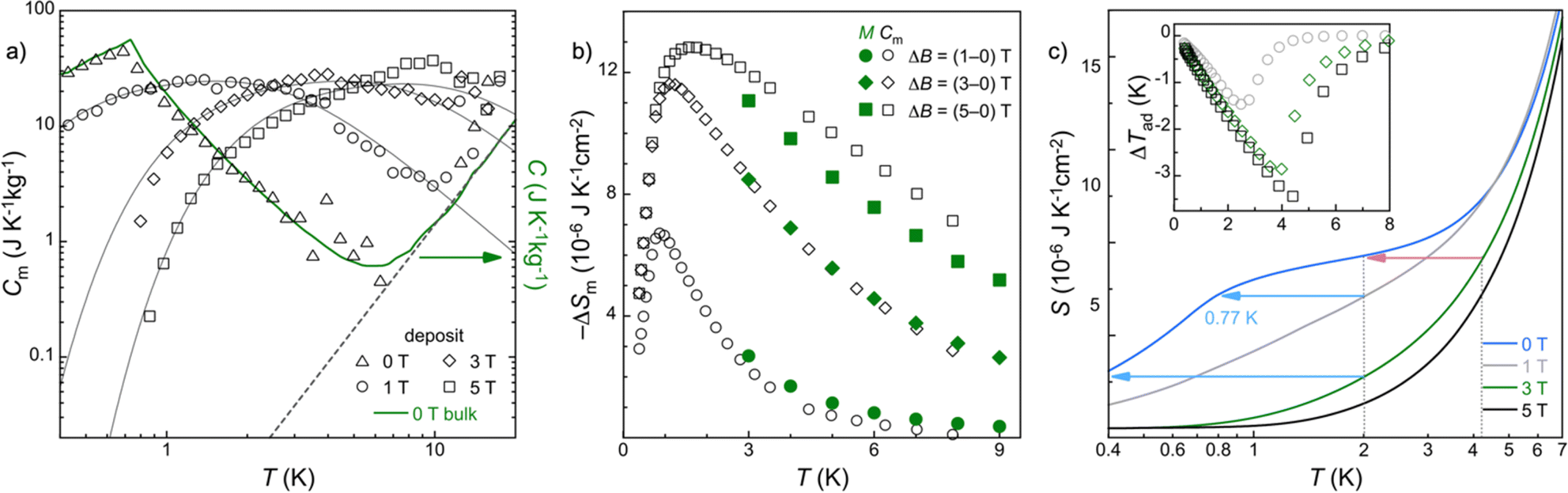 | ||
| Fig. 2 (a) Temperature dependence of Cm for a film of Gd formate particles spin-coated with the Si substrate at 50 °C for different applied fields B. The zero-field Cp data for bulk Gd(HCOO)3 is shown for comparison as a green line. Solid grey lines are calculated Schottky contributions for 1, 3 and 5 T. The dashed grey line is the lattice contribution calculated for a Debye temperature θD = 168 K.10a (b) Temperature dependence of −ΔSm per substrate area for different ΔB, derived from magnetic heat capacity and magnetization data. (c) Temperature dependence of the total S per substrate area at different fields for the {Si + Gd(HCOO)3 spin-coated film}. Arrows show the cooling produced by adiabatic demagnetization processes starting from either 2 or 4.2 K. Inset: temperature dependence of ΔTad for adiabatic demagnetizations from 1, 3, and 5 T. The x axis represents the starting temperature of the adiabatic process. | ||
We then studied the MCE characteristics of the Gd(HCOO)3 film spin-coated with the Si substrate at 50 °C. Using isothermal magnetization vs. field measured in the 2 to 10 K temperature range and Maxwell equations, we derived the magnetic entropy variations ΔSm resulting from different applied field changes ΔB, which are in excellent agreement with those reported for the bulk material (Fig. S26†).10a Expressed in surface units −ΔSm reaches for ΔB = 1 and 3 T values of 2.69 and 8.48 10−6 J K−1 cm2 at 3 K (Fig. 2b), which corresponds to 44.8 and 141.5 mJ K−1 cm3 mJ K−1 cm−3 respectively. As expected, these values are over 50 times higher than those estimated in the only previous report on the MCE per surface of MOF films.12 Alternatively, the magnetic entropy Sm can be determined using the magnetic component Cm of the heat capacity. Cm is calculated by subtracting the lattice contribution previously determined for the bulk material10a and the heat capacity of the Si, as determined experimentally under the same experimental conditions. Fig. 2a shows again the excellent agreement between data for the scaled deposit and bulk material. Applying a 1 T field is sufficient to cancel the magnetic order, and the Cm(T) data agree well with the Schottky contributions for an S = 7/2 system at all applied fields. From the Sm(T) curves derived by integration of the Cm data (Fig. S27†), both magnitudes defining the MCE, ΔSm, and ΔTad are then obtained numerically (Fig. 2b and c).
The change in magnetic entropy ΔSm of the deposits as determined through calorimetric and magnetic data for the lower 1 and 3 T fields (Fig. 2b) are overall in good agreement while being similar to those of the bulk material,10a altogether confirming the material's MCE is maintained in the deposit. To determine the cooling capacity of the spin-coated film, we now consider the total entropy S(T) data at the different applied fields for the {Si + film} entity, determined by integration of the as-measured total heat capacity (Fig. 2d). These indeed allow to predict the overall reduction in temperature that would result from adiabatic demagnetization processes (horizontal arrows in Fig. 2d).§ Thus, the spin-coated film deposited with the Si substrate at 50 °C would be able to cool itself and the 325 μm Si substrate down to 0.77 K from 2 K by removing a modest magnetic field of 1 T or from 4.2 K, i.e., liquid 4He bath temperature, removing a field of 5 T. Using a magnetic field of 3 T would allow cooling the substrate from 2 K to < 0.40 K, also in one demagnetization step. Alternatively, the deposit would cool its substrate from 4.2 K to below 1 K in just two adiabatic demagnetization steps, a first from 3 T and a second from 1 T, although this would require a step during which the heat generated by the application of the magnetic field is expelled through some kind of heat-switch/connection. While not unfeasible, this could be very challenging for a relatively soft and thin film such as those we report.
Conclusions
Homogeneous films of particles of the Gd(HCOO)3 MOF can be formed on unmodified silicon substrates by spin-coating formic acid dispersions. When the coating is made with the Si substrate at 50 °C, the film is continuous and ca. 5 times thicker, up to ca. 0.65 μm. As a result, this film provides an unprecedentedly high surface cooling capacity, thanks to the very high magnetocaloric performance of the bulk material, which is maintained once deposited. Indirect determination of the magnetic entropy and adiabatic temperature changes upon removal of an applied magnetic field show that the spin-coated film will be able to cool itself and a 325 μm thick Si wafer from 2 K or even from liquid He temperatures to <1 K by one sole demagnetization step under adiabatic conditions. This study demonstrates the potential of magnetic MOF films for local on-chip magnetic refrigeration to sub-K temperatures while providing an easy-to-use method to make such high-quality films.Data availability
All experimental data are available from the corresponding author upon fair request.Author contributions
I. T.: investigation, visualization, writing – review and editing; M. I. C.: investigation; J. G. L.: investigation, supervision; V. R. G.: investigation, supervision; I. G.: investigation, supervision, writing – review and editing; R. A.: supervision, funding acquisition, writing – review and editing; O. R.: conceptualization, investigation, visualization, supervision, funding acquisition, writing – original draft, writing – review and editing.Conflicts of interest
There are no conflicts to declare.Acknowledgements
The research described here was supported by the Spanish MICIN/AEI/10.13039/501100011033 and ERDF “A way of making Europe” (projects PID2019-105881RB-I00 and PID2020-1183294RB-I00) and the Aragón government (PLATON E31_20R and E31_23R, doctoral grant to IT). IT is grateful to Campus Iberus and Programa Ibercaja-CAI for supporting her research stay at KU Leuven. The authors acknowledge the Research Foundation Flanders (FWO Vlaanderen) for support in research projects G087422N and G85720N and the junior postdoctoral fellowships of JGL (12E5123N) and VRG (1263622N). KU Leuven is acknowledged for funding in research project C14/20/085.Notes and references
- A. J. Heinrich, W. D. Oliver, L. M. K. Vandersypen, A. Aradvan, R. Sessoli, D. Loss, A. Bleszynski Jayich, J. Fernandez-Rossier, A. Laucht and A. Morello, Nat. Nanotechnol., 2021, 16, 1318 CrossRef CAS PubMed; J. Clarke and F. K. Wilhelm, Nature, 2008, 453, 1031 CrossRef PubMed; M. H. Devoret and R. J. Schoelkopf, Science, 2013, 339, 1169 CrossRef PubMed.
- H. Cao, J. Low Temp. Phys., 2021, 204, 175 CrossRef CAS; J. M. Duval, T. Prouvé, P. Shirron, K. Shinozaki, Y. Sekimoto, T. Hasebe, G. Vermeulen, J. André, M. Hasumi, L. Montier and B. Mot, J. Low Temp. Phys., 2020, 199, 730–736 CrossRef.
- (a) A. Auffèves, The energetic footprint of quantum technologies is only starting to be tackled, see, PRX Quantum, 2022, 3, 020101 CrossRef; (b) IBM is developing a “super-fridge” specifically for future quantum computers but will still fall short, see https://www.ibm.com/quantum/blog/goldeneye-cryogenic-concept-system, consulted 29/02/2024; (c) C. Bucci, et al., large cryogenic set-ups are typically developed for particle physics applications, Prog. Part. Nucl. Phys., 2022, 122, 103902 CrossRef.
- F. Giazotto, T. T. Heikkilä, A. Luukanen, A. M. Savin and J. K. Pekola, Rev. Mod. Phys., 2006, 78, 217 CrossRef CAS; J. T. Muhonen, M. Meschke and J. P. Pekola, Rep. Prog. Phys., 2012, 75, 046501 CrossRef PubMed.
- (a) A. Cho, Science, 2009, 326, 778 CrossRef CAS PubMed; (b) Responding to the US Research Community's Liquid Helium Crisis, APS-MRS-ACS Science Policy report, https://www.aps.org/policy/reports/popa-reports/upload/HeliumReport.pdf; (c) D. Kramer, Phys. Today, 2023, 76, 18 Search PubMed.
- P. J. Shirron, Cryogenics, 2014, 62, 130 CrossRef CAS.
- V. Pecharsky and K. A. Gschneidner Jr, J. Magn. Magn. Mater., 1999, 200, 44 CrossRef CAS.
- J. Bartlett, G. Hardy, M. Whillock, M. Hailey, P. Coker, C. Theobald, I. D. Hepburn and A. Smith, Cryogenics, 2022, 128, 103592 CrossRef CAS.
- (a) M. Evangelisti, O. Roubeau, E. Palacios, A. Camón, T. N. Hooper, E. K. Brechin and J. J. Alonso, Angew. Chem., Int. Ed., 2011, 50, 6606 CrossRef CAS PubMed; (b) L.-X. Chang, G. Xiong, L. Wang, P. Cheng and B. Zhao, Chem. Commun., 2013, 49, 1055 RSC; (c) F.-S. Guo, Y.-C. Chen, L.-L. Mao, W.-Q. Li, J.-D. Leng, R. Tarasenko, M. Orendác, J. Prokleska, V. Schovsky and M.-L. Tong, Chem.–Eur. J., 2013, 19, 14876 CrossRef CAS PubMed.
- (a) G. Lorusso, J. W. Sharples, E. Palacios, O. Roubeau, E. K. Brechin, R. Sessoli, A. Rossin, F. Tuna, E. J. L. McInnes, D. Collison and M. Evangelisti, Adv. Mater., 2013, 25, 4653 CrossRef CAS PubMed; (b) R. Sibille, T. Mazet, B. Malaman and M. François, Chem.–Eur. J., 2012, 18, 12970 CrossRef CAS PubMed; (c) G. Lorusso, M. A. Palacios, G. S. Nichol, E. K. Brechin, O. Roubeau and M. Evangelisti, Chem. Commun., 2012, 48, 7592 RSC; (d) Y.-C. Chen, L. Qin, Z.-S. Meng, D.-F. Yang, C. Wu, Z. Fu, Y.-Z. Zheng, J.-L. Liu, R. Tarasenko, M. Orendác, J. Prokleska, V. Sechosky and M.-L. Tong, J. Mater. Chem. A, 2014, 2, 9851 RSC; (e) C. Das, A. Upadhyay, K. Uddin Ansari, N. Ogiwara, T. Kitao, S. Horike and M. Shanmugam, Inorg. Chem., 2018, 57, 6584 CrossRef CAS PubMed.
- J. A. Barclay and W. A. Steyert, Cryogenics, 1982, 22, 73 CrossRef CAS; P. Wikus, et al. , Cryogenics, 2014, 62, 150 CrossRef.
- G. Lorusso, E. Natividad, M. Evangelisti and O. Roubeau, Mater. Horiz., 2019, 6, 144 RSC.
- S. Kumar, G. Gabarró Riera, A. Arauzo, J. Hrubý, S. Hill, L. Bogani, J. Rubio-Zuazo, J. Jover, E. Bartolomé and E. C. Sañudo, J. Mater. Chem. A, 2024, 12, 6269 RSC.
- See for example (a) D. Wang and H. Möhwald, Adv. Mater., 2004, 16, 244 CrossRef CAS; (b) T. O. Løveng Sunde, E. Garskaite, B. Otter, H. E. Fossheim, R. Sæterli, R. Holmestad, M.-A. Einarsrud and T. Grande, J. Mater. Chem., 2012, 22, 15740 RSC.
- I. Tejedor, A. Urtizberea, E. Natividad, J. I. Martínez, I. Gascón and O. Roubeau, Mater. Horiz., 2023, 10, 5214 RSC.
- D. E. Kravchenko, A. J. Cruz, S. Rodríguez-Hermida, N. Wauteraerts, T. Hauffman and R. Ameloot, Chem. Mater., 2020, 32, 10469 CrossRef CAS.
- (a) V. K. LaMer and R. H. Dinegar, J. Am. Chem. Soc., 1950, 72, 48478 CrossRef; (b) V. K. LaMer, Ind. Eng. Chem., 1952, 44, 1270 CrossRef CAS; (c) D. B. K. Chu, J. S. Owen and B. Peters, J. Phys. Chem. A, 2017, 121, 7511 CrossRef CAS PubMed.
- A. P. de Sousa, A. K. Barbosa da Silva, L. R. Fernandes Figueiredo, E. Souto de Medeiros, T. A. Passos, D. Ferreira de Oliveira and D. Guedes de Lima Cavalcante, Mater. Res. Express, 2022, 9, 116404 CrossRef CAS.
Footnotes |
| † Electronic supplementary information (ESI) available: Experimental details, additional SEM observations, DLS, PXRD and magneto-thermal data. See DOI: https://doi.org/10.1039/d4ta03541k |
‡ Using the Scherrer equation τ = Kλ/β![[thin space (1/6-em)]](https://www.rsc.org/images/entities/i_char_2009.gif) cosθ, where τ is the mean size of crystalline domains, and using the 20 peak at 2θ = 17.35°, its estimated FWHM of 0.51° as line broadening β, K = 0.89 and λ = 1.54 Å (Cu Kα). cosθ, where τ is the mean size of crystalline domains, and using the 20 peak at 2θ = 17.35°, its estimated FWHM of 0.51° as line broadening β, K = 0.89 and λ = 1.54 Å (Cu Kα). |
| § One important aspect for this is an efficient heat transfer through the Si substrate and the sapphire sample platform of the setup (see Scheme S1 and Fig. S28†). |
| This journal is © The Royal Society of Chemistry 2024 |