
 Open Access Article
 This Open Access Article is licensed under a Creative Commons Attribution-Non Commercial 3.0 Unported Licence
Hydrogen absorption boosting in mildly annealed bulk MoS2†
Jairo
Obando-Guevara
 *ab,
Álvaro
González-García
a,
Marcin
Rosmus
c,
Natalia
Olszowska
c,
César
González
ad,
Guillermo
Morón-Navarrete
a,
Jun
Fujii
e,
Antonio
Tejeda
b,
Miguel Ángel
González-Barrio
a and
Arantzazu
Mascaraque
a
*ab,
Álvaro
González-García
a,
Marcin
Rosmus
c,
Natalia
Olszowska
c,
César
González
ad,
Guillermo
Morón-Navarrete
a,
Jun
Fujii
e,
Antonio
Tejeda
b,
Miguel Ángel
González-Barrio
a and
Arantzazu
Mascaraque
a
aDto. de Física de Materiales, Universidad Complutense de Madrid, 28040 Madrid, Spain. E-mail: jairoban@ucm.es
bLaboratoire de Physique des Solides, CNRS, Université Paris-Saclay, 91405 Orsay, France
cNational Synchrotron Radiation Centre SOLARIS, Jagiellonian University, Czerwone Maki 98, PL-30392 Kraków, Poland
dInstituto de Magnetismo Aplicado UCM-ADIF, E-28232 Las Rozas de Madrid, Spain
eIstituto Officina dei Materiali (IOM)-CNR, Laboratorio TASC, I-34149 Trieste, Italy
First published on 20th July 2024
Abstract
The basal plane of MoS2 has been considered a potential source of active catalytic sites in hydrogen absorption. Sulfur vacancies can activate the inert basal plane of MoS2; however, achieving sufficient catalytic efficiency requires a high defect concentration of about 12%. We investigated the effect of defects on the hydrogen adsorption on the basal plane of MoS2 using angle-resolved photoemission spectroscopy (ARPES) and density functional theory (DFT) calculations. Mild annealing in terms of temperature and time effectively introduces single sulfur vacancy (VS) defects, as observed from the electronic structural changes that are in excellent agreement with DFT calculations for a VS concentration of ∼4%. Subsequent exposure to molecular hydrogen showed that the higher hydrogen pressure facilitates hydrogen adsorption, as predicted by theoretical calculations. Interestingly, hydrogen exposure restores the electronic structure to a state similar to that of pristine MoS2. These results suggest that the controlled introduction of VS defects via annealing is a promising strategy for enhancing hydrogen adsorption on MoS2, paving the way for its potential use in future catalytic applications.
1. Introduction
High-efficiency devices for renewable and sustainable energy conversion are essential to reduce dependence on conventional fossil fuels and address global environmental and resource challenges.1–5 Hydrogen, a clean fuel and energy carrier, is currently enjoying unprecedented political favour and business momentum, with a rapidly increasing number of policies around the world and being at the core of the circular economy.6 Addressing the challenges of hydrogen implementation as an alternative fuel could significantly mitigate greenhouse gas emissions and have a positive environmental impact.7Electrochemical water splitting (WS) stands out as one of the most eco-friendly approaches for hydrogen production.8–10 This process involves two half-reactions: hydrogen evolution reaction (HER: 2H+ + 2e− → H2) occurring at the cathode and oxygen evolution reaction (OER: 2H2O → O2 + 4H+ + 4e−) at the anode.11,12 Catalysts play a crucial role in enhancing the efficiency of electrochemical devices by speeding up reactions and reducing the required energy input.8–10 Although platinum group metals (PGMs) are often used as catalysts due to their exceptional performance in a wide range of applications, there is a strong interest in finding alternative catalysts for economic, environmental, and technological reasons.13,14
MoS2 has emerged as a promising alternative for PGMs in the HER, driven by various advantageous features.15,16 Its catalytic activity can be modulated by altering its structure through diverse approaches, such as layer number manipulation,17 Mo-edge exposure,18–20 nanostructuring,21–24 phase engineering,25 doping with metal-26,27 and non-metal atoms28,29 or defect introduction,30 thereby rendering it adaptable to specific requirements. Furthermore, MoS2 demonstrates stability under a broad range of electrochemical conditions, retaining its catalytic performance even in harsh environments.31–33
Defects play a pivotal role in MoS2, significantly impacting its physicochemical properties and offering a rich test field for tailoring and introducing new functionalities. Notably, single sulfur vacancies (VS) at the basal plane have been identified as catalytic centres for the adsorption of hydrogen intermediates.34–37 VS is the most prevalent defect in MoS2 since its enthalpy of formation is the lowest compared to that of other defects.38–40 This indicates that VS has a lower tendency to combine. Additionally, Mo and S antisites are rarely observed due to their higher enthalpies of formation.41 However, achieving good catalytic efficiency requires a high defect concentration of approximately 12% under normal conditions.34,35 The approaches described above for adjusting the catalytic activity of MoS2 vary in complexity. Among these, thermal annealing is recognized as the most straightforward for generating VS. Thermal annealing, yielding S sublimation in the basal plane, has been previously reported for single-layered42–45 and bulk46 MoS2. The threshold temperature at which the defect-related effects are observed in a single layer is 200 °C. While for the bulk case, a threshold temperature is less known. No signs of defect-related effects are observed below 400 °C,42 whereas surface defects have been observed microscopically at 650 °C.46 These studies consistently employ temperatures below 900 °C, which is the point at which MoS2 degradation begins.47 It is important to consider that, the annealing treatment in previous works typically maintain the target temperature for periods ranging from 30 (ref. 43 and 45) to 120 (ref. 44) minutes, after which defect-related effects become evident.
In this study, we investigated the role of S defects and the underlying physical mechanisms driving the enhancement of hydrogen adsorption on the MoS2 basal plane. To this end, we employed mild annealing, i.e. at a relatively low temperature and of short duration, under ultra-high vacuum as a simple and reliable method to create S defects in the basal plane. We monitored the appearance of novel spectral signatures in the band structure upon defect creation and further hydrogen exposure using angle-resolved photoemission spectroscopy (ARPES). The comparison of the experimental results with density functional theory (DFT) band structure calculations for pristine and VS-defective MoS2 before and after hydrogenation allows us to identify which electronic states are involved in hydrogen absorption boosting.
2. Methods
2.1. Sample preparation
The samples used were synthetic bulk-like p-doped 2H-MoS2 (Nb concentration ∼ 2 × 1017 cm−3) crystals from 2DSemiconductors, 3 × 3 mm2 approx. in the lateral size. Structural and morphological information, including photoluminescence, Raman spectroscopy, X-ray diffraction and transmission electron microscopy, is available elsewhere.48 Three samples were exfoliated in an ultra-high vacuum (UHV) chamber at a pressure of 5 × 10⁻⁸ mbar, which produces flat surfaces with large terrace widths. Following exfoliation, the samples were transferred to a preparation chamber (base pressure ∼ 2 × 10⁻¹⁰ mbar). Any possible surface adsorbates were removed by a cleaning method that involved annealing with a resistive heater at 150 °C for 15 min (temperature was monitored with a thermocouple attached to the back of a sample holder). Controlled annealing was performed by electron bombardment (temperature was monitored with a calibrated pyrometer aimed at the sample surface centre). The increasing temperature ramp lasted Δt = 10 min and the final temperature preparation was kept constant for 5 min. The hydrogenation treatment involved exposing the samples to pure H2 (purity better than 99.999%). For this purpose, a preparation chamber operating at room temperature (RT) and a base pressure below 5 × 10⁻¹⁰ mbar was filled with hydrogen up to a target partial pressure. Total exposures were achieved by maintaining a constant H2 partial pressure while varying the exposure time. The exposures are expressed in Langmuir units (L).2.2. ARPES
ARPES measurements were performed at the URANOS beamline of the SOLARIS National Synchrotron Radiation Centre (Krakow, Poland) and the APE-LE beamline at ELETTRA Sincrotrone (Trieste, Italy). All spectra were measured using light linearly polarised in the horizontal plane with a photon energy of hν = 70 eV and at a temperature of 110 K. The maximum beamline spot size was 65 × 130 μm2 (vertical and horizontal, respectively). Photoelectrons were collected using a Scienta Omicron DA30-L electron spectrometer with energy and angle resolutions better than 16 meV and 0.1°, respectively. The Fermi level was determined by measuring a poly-crystalline Au mounted in electrical contact with the sample. As MoS2 is semiconducting, we employed the standard approach to give any energy reference or displacement with respect to the valence band maximum (VBM) (see Fig. S1c† for the determination of the VBM).2.3. DFT calculations
DFT calculations were performed using the plane-wave Quantum ESPRESSO (QE) package.49 We used the generalized gradient approximation (GGA) developed by Perdew–Burke–Ernzerhof (PBE) for the exchange and correlation functional50 as well as the projector-augmented wave (PAW) pseudo-potentials.51 The cut-off used for the plane waves was 49 Ry. The calculations converged until the difference in the energy (force) was less than 5 × 10⁻⁵ Ry (4 × 10⁻⁴ Ry per bohr radius). The pristine band structure was calculated before simulating the VS inclusion and hydrogen exposure. The pristine monolayer structure consisted of a S–Mo–S trilayer (a MoS2 single-layer) with 1 × 1 periodicity. We included a vacuum of 15 Å to reduce the interaction between neighbouring layers. The two-dimensional first Brillouin zone (1BZ) k-mesh has a 12 × 12 size. The lattice parameter obtained was 3.167 Å, leading to a band structure with a direct band gap of 1.8 eV at the K point. To simulate the VS defects, we expanded the periodicity of the pristine structure to a 5 × 5 supercell by removing one atom from the cell. This situation corresponds to a 4% VS concentration. Once we had created the vacancy, we introduced H2 molecules around. The calculations with the larger size used 16 k-points in the 1BZ. With the relaxed structures, we calculate the corresponding band structure of the 5 × 5 supercell using now 91 k-points along the M–G–K direction. To compare the calculations with the experimental results, we converted the supercell band structure into unfolded bands in the 1 × 1 unit cell with the extensively used unfolding methodology explained before52 and implemented in the unfold-x code, suitable for the QE package.3. Results and discussion
Fig. 1a shows the 2H-MoS2 structure consisting of a hexagonal unit cell of two rotated hexagonal S–Mo–S trilayers (space group symmetry is P63/mmc). In this structure, the Mo atoms of one layer are covalently bonded to the neighbouring S atoms layers. S–Mo–S trilayers (hereafter referred to as single-layers) are bonded to each other by van der Waals (vdW) forces and stack to form the bulk. Fig. 1b presents the BZ and the projected BZ of the reciprocal space.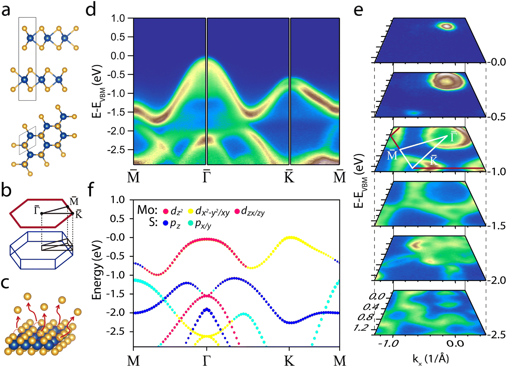 | ||
Fig. 1 (a) Side and top view of the 2H-MoS2 crystalline structure. Mo atoms (blue) and S atoms (orange). (b) Hexagonal BZ (dark blue line) and its high-symmetry points. On top, we depict the projected BZ (red line). (c) Schematic representation of VS defects generation by thermal annealing. (d) ARPES intensity showing the MoS2 band structure along the  high-symmetry points path. (e) Stack of constant energy maps at different binding energies. (f) DFT orbital-projected band structure calculated for a single-layer of MoS2 along the MΓKM path. The symbol size is proportional to the weight of the state. high-symmetry points path. (e) Stack of constant energy maps at different binding energies. (f) DFT orbital-projected band structure calculated for a single-layer of MoS2 along the MΓKM path. The symbol size is proportional to the weight of the state. | ||
Panel d in Fig. 1 shows the valence band (VB) of a Nb-doped MoS2 sample. The strong dispersion features two minima, about halfway between the M and Γ points and between the Γ and K points. Notably, Nb doping does not alter the electronic structure shape;53 however, it induces a significant p-type rigid shift of ∼0.63 eV in the electronic band structure, placing the VBM very close to the Fermi level (see Fig. S1 and S2†). Doping with Nb has a beneficial effect on hydrogen adsorption by bringing the d-band centre closer to the Fermi level,27,54 thereby reducing the free energy of hydrogen adsorption on the basal plane.55 In addition, the increased conductivity mitigates sample charge problems, ensuring reliable ARPES measurements.
The electronic structure around the K point shows spin–orbit splitting (160 meV), indicating the high crystalline quality of the samples56 (see Fig. S1d†). Unlike single-layer MoS2, in bulk MoS2 the VBM is at the Γ point, leading to an indirect band gap of 1.2 eV (the Γ point is ∼0.6 eV higher than the K point).56,57 As a result, the constant energy contour plots shown in Fig. 1e present the characteristic circle and triangles centred at the Γ and K points, highlighting the crystalline symmetry.
To identify the orbital origin of the VB, in Fig. 1f we display the VB orbital projection calculated for a single-layer of MoS2. The top band is dominated by Mo d orbitals ranging from dz2 at the Γ point to dx2+y2/dxy near the K point. In contrast, the two adjacent bands at higher binding energy mainly consist of S p orbitals. Knowing the orbital origin of the bands is crucial in elucidating the physical origin of the changes observed after annealing and hydrogenation.
The electronic structures upon annealing at 600 °C and 700 °C are displayed in Fig. 2. We focus on the ΓK direction, as this is the region that exhibits the relevant changes. The quality of the ARPES maps demonstrates that annealing at these temperatures effectively preserves the overall crystallinity of the sample. This preservation is particularly evident at the K point, where the spin splitting remains well resolved.56
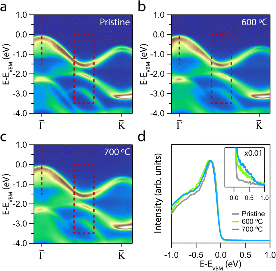 | ||
Fig. 2 ARPES intensity showing the evolution of the MoS2 dispersion along the  direction after annealing: (a) pristine, (b) 600 °C and (c) 700 °C. The dashed lines and rectangles mark the regions from which EDCs are taken. (d) EDCs at direction after annealing: (a) pristine, (b) 600 °C and (c) 700 °C. The dashed lines and rectangles mark the regions from which EDCs are taken. (d) EDCs at ![[capital Gamma, Greek, macron]](https://www.rsc.org/images/entities/i_char_e0ba.gif) integrated over a Δk = 0.1 A−1. The EDCs of the annealed samples were shifted towards their respective pristine VBM for comparison. Inset: enlarged region near the VBM, all the EDCs are multiplied by 0.01. integrated over a Δk = 0.1 A−1. The EDCs of the annealed samples were shifted towards their respective pristine VBM for comparison. Inset: enlarged region near the VBM, all the EDCs are multiplied by 0.01. | ||
Although qualitative changes are apparent in the marked regions, a deeper insight into the effect of annealing is obtained by analyzing the energy dispersion curves (EDCs). Fig. 2d presents the EDCs centred at Γ of the annealed samples. A distinctly sharp VB edge can be observed, indicating the crystallinity preservation following the annealing treatments. However, while the EDC of the pristine sample exhibits a steep drop, a gradual emergence of tail states can be noted for each of the annealed samples. According to the Anderson model, a disordered lattice structure leads to the formation of localised electronic states immediately above (below) the valence (conduction) band.58,59 This tail states constitutes an exponentially decaying density of states that extends into the gap59,60 that we can assign to the generation of defects.61,62
The formation of VS implies a broken Mo–S bond, so regions of the reciprocal space with well-differentiated S p and Mo d orbital contributions are more likely to show modifications. Thus, the region prone to exhibit changes due to the presence of VS is marked with a dashed red rectangle in Fig. 2. Fig. 3a and b shows a set of EDCs taken in this region corresponding to the 600 °C and 700 °C annealing samples. The set of EDCs of the pristine sample is added for comparison. It is seen that some shoulders appear, marked with ticks, as shown in the figure. The intensity of these shoulders is more prominent at an annealing temperature of 700 °C. The appearance of such features in this region indicates that the annealing does not affect the entire band structure equally.
 | ||
| Fig. 3 (a and b) Set of EDCs corresponding to the rectangle regions marked in Fig. 2 for annealing at 600 °C and 700 °C, respectively. The black curves correspond to the pristine sample. (c) DFT orbital-projected electronic band structure calculated for a single-layer of MoS2 with 4% of VS. (d) Set of theoretical EDCs taken from the dashed rectangle regions in (c), corresponding to the sum of the Mo d and S p orbitals. The orbital projection of the central EDC is shown in (e). | ||
To better understand the observed modifications after the annealing, Fig. 3c presents the orbital contribution of the band structure calculated for a single-layer of MoS2 with 4% of VS. To compare with the experimental results, we display in Fig. 3d a set of EDCs from a region analogous to the red dashed rectangles. The figure shows the development of a shoulder in the same place as those observed in the experimental bands. Furthermore, Fig. 3e presents the orbital projection of the marked EDCs in the set. The shoulder formation appears in the S p orbital after the introduction of VS and it is absent in the pristine sample band structure (the calculation of the pristine band structure is presented in Fig. S3a†). In addition, the Mo d orbital hardly shows any change. This remarkable agreement between the experimental and theoretical results indicates not only the presence of VS in the annealed samples but also points to the S p orbital origin of the observed electronic structure changes. The amount of 4% of VS has been selected for the theory to obtain good agreement with the experimental results. Therefore, it suggests that the density of defects obtained after annealing should be around the same order. Moreover, no changes in the chemical composition of the sample could be detected by X-ray photoemission spectroscopy (XPS) for such a low defect concentration.30
After revealing how the creation of sulfur defects modifies the VB, we exposed the annealed samples to H2 to evaluate their reactivity at two different pressures. Two samples annealed at 700 °C were dosed up to 1000 L at RT and pressures of 1 × 10⁻⁴ mbar (hereafter referred to as “high pressure”) and 1 × 10⁻⁶ mbar (hereafter referred to as “low pressure”). Fig. 4a shows the ARPES intensity of the sample dosed at high pressure. A new spectral weight below 0 eV binding energy was observed. Fig. 4b presents an EDC at the Γ point, highlighting the appearance of a well-defined intensity step. The formation of this step at the Fermi energy across the entire BZ is shown in Fig. S4† and it induces a −0.17 eV downward n-type shift of the VB. The retrieval of the “pristine” electronic structure after hydrogenation, as it is seen in panel a, provides additional experimental evidence of hydrogen incorporation and bond formation into the VS. This effect is consistent with the “VS passivation” observed in MoS2.63,64 Unlike other previous works,63 we have not detected any ambipolar VB or band replicas after hydrogenation.
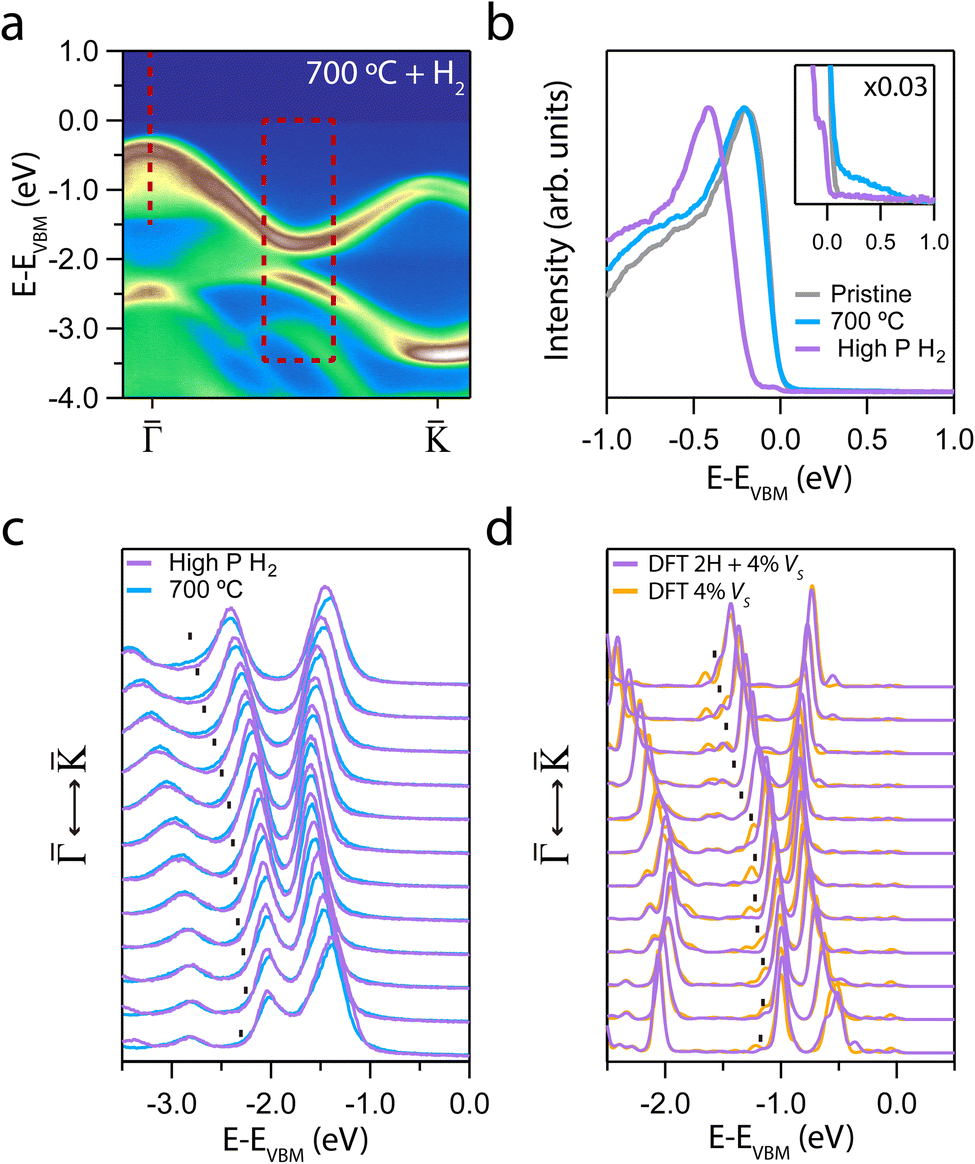 | ||
Fig. 4 (a) ARPES intensity showing the evolution of the MoS2 dispersion along the  direction for the annealed sample at 700 °C after exposure to 1000 L of H2 at a pressure of 1 × 10⁻⁴ mbar (relative high pressure). (b) EDC at of the hydrogenated sample taken from (a). Inset: enlarged region near the VBM, all the EDCs are multiplied by 0.03. (c) Set of EDCs taken from the dashed rectangle regions in (a). (d) Set of theoretical EDCs taken from the dashed rectangle region in Fig. S3b.† direction for the annealed sample at 700 °C after exposure to 1000 L of H2 at a pressure of 1 × 10⁻⁴ mbar (relative high pressure). (b) EDC at of the hydrogenated sample taken from (a). Inset: enlarged region near the VBM, all the EDCs are multiplied by 0.03. (c) Set of EDCs taken from the dashed rectangle regions in (a). (d) Set of theoretical EDCs taken from the dashed rectangle region in Fig. S3b.† | ||
Fig. 4c displays the set of EDCs corresponding to the rectangular region marked in panel a. Surprisingly, the shoulders due to the presence of VS are suppressed and the overall band structure exhibits increased sharpness after hydrogenation. This experimental observation is in good agreement with the DFT calculation with H atoms adsorbed on a single layer of MoS2 with 4% of VS (see Fig. S3b†). Fig. 4d presents a set of theoretical EDCs taken from Fig. S3b.† A comparison between the theoretical and the experimental data reveals an identical suppression of the shoulder intensity maxima.
Calculations indicate that molecular hydrogen chemisorbs dissociatively near a VS only under high H2 pressure at RT.65 Molecular hydrogen physisorbs on the surface when there are no sulphur vacancies. Furthermore, the molecule remains in the same orientation over a VS at 0 K temperature. Increasing the temperature leads to desorption of the isolated molecule. Including other H2 molecules facilitates its rotation and leads to molecular dissociation. In this situation, the H atoms remain linked to the Mo atoms. At high pressure, the energy barrier disappears, favouring the dissociative process (see Sec. III of ESI† for more details). Our experimental findings suggest that the high H2 pressure yields a much larger dissociative chemisorption that can thus be explained within this theoretical scenario. For similar H2 exposure but at lower pressure, minimal changes in the band structure were observed (see Fig. S5†).
The appearance of a Fermi step after hydrogenation, showing a transition from semiconducting to a metallic surface upon hydrogen adsorption has been reported in other semiconductors, including Ge(111),66 Si-terminated n- and p-doped β-SiC(100),67 SrTiO3(001),68 and ZnO(1010).69 Similar to these semiconductors, the formation of a metallic Fermi step and the n-type shift of the VB in MoS2 indicates that the VS present in the annealed sample can adsorb and dissociate H2. VS is either in neutral or negative charge state and acts as an acceptor.38 The adsorption of hydrogen involves the formation of Mo–H bonds, facilitating charge transfer from the adsorbate to the surface. The removal of sulfur causes an excess of electrons on the Mo atoms, which is compensated through hydrogen bonding, thereby enhancing overall surface stability.
The HER activity for S defect concentrations between 2 and 22% has been studied in previous works.34,35 Our results indicate that a high concentration of VS is not necessary to observe significant changes in the electronic structure. Conversely, our results are consistent with the observation that a high density of S defects leads to an inert basal plane for hydrogen adsorption, and consequently a low HER activity.34,35,70 This comparison also highlights the dissociative capability of VS defects compared to other types of defects.
4. Conclusions
We investigated the effect of sulfur vacancies upon hydrogen adsorption on the basal plane of Nb-doped MoS2 bulk crystals exfoliated in UHV. Our work demonstrates that mild annealing induces distinctive changes in the band structure, that can be clearly attributed to the generation of sulfur defects at low concentrations. The observed changes in EDCs that mainly probe S p and Mo d orbitals are in perfect agreement with the DFT calculations of MoS2 with 4% of VS defects. This highlights the effectiveness of annealing as a simple, efficient and reproducible method to generate sulfur vacancies in the basal plane.In situ exposure of the S-defective samples to H2 adsorption causes a charge transfer from the adsorbate to the surface and restores the electronic structure to resemble the pristine state. The hydrogenation at high-pressure results in the metallisation of the surface, evidenced by a well-defined Fermi-like step close to the VBM. On the other hand, hydrogen exposure at low pressure has a similar but less dramatic effect on the band structure, indicating that the partial hydrogen pressure is more relevant in the H2 absorption than VS defect concentration. From theoretical calculations, we can conclude that high pressure accelerates the hydrogen adsorption kinetics, shifting the equilibrium towards more adsorbed molecules and explaining the observed differences between high and low H2 partial pressures (even when large doses were used in both cases).
Our results demonstrate that mild annealing can effectively enhance hydrogen adsorption. The significant dreceasing in the annealing time has positive implications for the reduction of energy resources needed to transform MoS2 into a catalytically active material. In this sense, the relatively “high” hydrogen pressure required to enhance dissociation and adsorption is an advantage in real catalytic reactions in industry, where the working conditions are far from UHV experiments.
Data availability
The data that support the findings of this study are openly available at https://zenodo.org/doi/10.5281/zenodo.12659310.Author contributions
A. M. and M. A. G.-B. conceived, coordinated and designed the experiments, J. O.-G., Á. G.-G., A. M., M. A. G.-B., N. O., M. R. and J. F. conducted the experiments and collected the data, J. O.-G., Á. G.-G., A. T., A. M. and M. A. G.-B. analyzed the data. C. G. and G. M.-N. realized the theoretical calculations. All the authors contributed to the writing and provided critical revisions to the manuscript.Conflicts of interest
The authors declare no competing financial interest.Acknowledgements
M. Á. G.-B. and A. M. thank the Ministerio de Ciencia e Innovación (project PID2020-117024GB-C43) and Comunidad de Madrid (project S2108-NMT4321) for financial support. A. T. acknowledges the support from the French Agence Nationale de la Recherche (ANR) contract ref. NT-09-618999 and DIMAG project from 2019 FLAG-ERA call. Á. G.-G. thanks Universidad Complutense de Madrid and Banco Santander (CT82/20–CT83/20) for financial support. N. O. and M. R. thank the Polish Ministry and Higher Education Project Support contract No. 1/SOL/2021/2. C. G. and G. M.-N. acknowledge the Spanish Supercomputing Network (RES) for the computational resources provided at Altamira (IFCA) through the projects: FI-2023-2-0022 and FI-2023-1-0016 and the financial support by the Spanish Ministry of Research, Innovation and Universities, project: PID2021-123112OB-C21. We acknowledge SOLARIS Center and ELETTRA Sincrotrone for the access to the beamline URANOS and APE-LE, respectively.References
- S. Yuan, X. Duan, J. Liu, Y. Ye, F. Lv, T. Liu, Q. Wang and X. Zhang, Energy Storage Mater., 2021, 42, 317 CrossRef.
- J. Tang, H. Ni, R.-L. Peng, N. Wang and L. Zuo, J. Power Sources, 2023, 562, 232785 CrossRef CAS.
- S. Kandpal, T. Ghosh, C. Rani, A. Chaudhary, J. Park, P. S. Lee and R. Kumar, ACS Energy Lett., 2023, 8, 1870 CrossRef CAS.
- Y. Zhao, H. Liu, Y. Yan, T. Chen, H. Yu, L. O. Ejeta, G. Zhang and H. Duan, Energy Environ. Mater., 2023, 6, e12303 CrossRef CAS.
- M. K. Debe, Nature, 2012, 486, 43 CrossRef CAS PubMed.
- N. Farrell, Renewable Sustainable Energy Rev., 2023, 178, 113216 CrossRef CAS.
- M. Ball and M. Wietschel, Int. J. Hydrogen Energy, 2009, 34, 615 CrossRef CAS.
- Q. Qian, Y. Zhu, N. Ahmad, Y. Feng, H. Zhang, M. Cheng, H. Liu, C. Xiao, G. Zhang and Y. Xie, Adv. Mater., 2024, 36, 2306108 CrossRef CAS.
- S. Y. Tee, K. Y. Win, W. S. Teo, L.-D. Koh, S. Liu, C. P. Teng and M.-Y. Han, Adv. Sci., 2017, 4, 1600337 CrossRef.
- Z. W. Seh, J. Kibsgaard, C. F. Dickens, I. Chorkendorff, J. K. Nørskov and T. F. Jaramillo, Science, 2017, 355, eaad4998 CrossRef PubMed.
- N. Krstajić, M. Popović, B. Grgur, M. Vojnović and D. Šepa, J. Electroanal. Chem., 2001, 512, 16 CrossRef.
- J. K. Nørskov, T. Bligaard, A. Logadottir, J. R. Kitchin, J. G. Chen, S. Pandelov and U. Stimming, J. Electrochem. Soc., 2005, 152, J23 CrossRef.
- I. E. L. Stephens, J. Rossmeisl and I. Chorkendorff, Science, 2016, 354, 1378 CrossRef CAS.
- B. J. Glaister and G. M. Mudd, Miner. Eng., 2010, 23, 438 CrossRef CAS.
- A. Mondal and A. Vomiero, Adv. Funct. Mater., 2022, 32, 2208994 CrossRef CAS.
- Q. Fu, J. Han, X. Wang, P. Xu, T. Yao, J. Zhong, W. Zhong, S. Liu, T. Gao, Z. Zhang, L. Xu and B. Song, Adv. Mater., 2021, 33, 1907818 CrossRef CAS.
- B. Seo, G. Y. Jung, Y. J. Sa, H. Y. Jeong, J. Y. Cheon, J. H. Lee, H. Y. Kim, J. C. Kim, H. S. Shin, S. K. Kwak and S. H. Joo, ACS Nano, 2015, 9, 3728 CrossRef CAS.
- N. P. Kondekar, M. G. Boebinger, E. V. Woods and M. T. McDowell, ACS Appl. Mater. Interfaces, 2017, 9, 32394 CrossRef CAS.
- D. Kong, H. Wang, J. J. Cha, M. Pasta, K. J. Koski, J. Yao and Y. Cui, Nano Lett., 2013, 13, 1341 CrossRef CAS PubMed.
- H. Wang, Z. Lu, S. Xu, D. Kong, J. J. Cha, G. Zheng, P.-C. Hsu, K. Yan, D. Bradshaw, F. B. Prinz and Y. Cui, Proc. Natl. Acad. Sci. U. S. A., 2013, 110, 19701 CrossRef CAS.
- Q. Zhou, S. Su, P. Cheng, X. Hu, X. Gao, Z. Zhang and J.-M. Liu, J. Mater. Chem. C, 2020, 8, 3017 RSC.
- T. H. Ly, J. Zhao, H. Kim, G. H. Han, H. Nam and Y. H. Lee, Adv. Mater., 2016, 28, 7723 CrossRef CAS PubMed.
- J. Kibsgaard, Z. Chen, B. N. Reinecke and T. F. Jaramillo, Nat. Mater., 2012, 11, 963 CrossRef CAS PubMed.
- B. Guo, K. Yu, H. Li, H. Song, Y. Zhang, X. Lei, H. Fu, Y. Tan and Z. Zhu, ACS Appl. Mater. Interfaces, 2016, 8, 5517 CrossRef CAS.
- Y. Zhang, L. Wang, Q. Chen, J. Cao and C. Zhang, Front. Chem., 2022, 10, 1000406 CrossRef CAS PubMed.
- H. Li, S. Wang, H. Sawada, G. G. D. Han, T. Samuels, C. S. Allen, A. I. Kirkland, J. C. Grossman and J. H. Warner, ACS Nano, 2017, 11, 3392 CrossRef CAS PubMed.
- M. Chhetri, U. Gupta, L. Yadgarov, R. Rosentsveig, R. Tenne and C. N. R. Rao, ChemElectroChem, 2016, 3, 1937 CrossRef CAS.
- X. Xu, Z. Peng, H. Xu and D. Cheng, J. Catal., 2022, 416, 47 CrossRef CAS.
- W. Xiao, P. Liu, J. Zhang, W. Song, Y. P. Feng, D. Gao and J. Ding, Adv. Energy Mater., 2017, 7, 1602086 CrossRef.
- L. Li, Z. Qin, L. Ries, S. Hong, T. Michel, J. Yang, C. Salameh, M. Bechelany, P. Miele, D. Kaplan, M. Chhowalla and D. Voiry, ACS Nano, 2019, 13, 6824 CrossRef CAS PubMed.
- Y.-C. Chen, A.-Y. Lu, P. Lu, X. Yang, C.-M. Jiang, M. Mariano, B. Kaehr, O. Lin, A. Taylor, I. D. Sharp, L.-J. Li, S. S. Chou and V. Tung, Adv. Mater., 2017, 29, 1703863 CrossRef PubMed.
- R. V. Mom, J. N. Louwen, J. W. M. Frenken and I. M. N. Groot, Nat. Commun., 2019, 10, 2546 CrossRef PubMed.
- N. Abidi, A. Bonduelle-Skrzypczak and S. N. Steinmann, J. Phys. Chem. C, 2021, 125, 17058 CrossRef CAS.
- H. Li, C. Tsai, A. L. Koh, L. Cai, A. W. Contryman, A. H. Fragapane, J. Zhao, H. S. Han, H. C. Manoharan, F. Abild-Pedersen, J. K. Nørskov and X. Zheng, Nat. Mater., 2016, 15, 48 CrossRef CAS PubMed.
- G. Li, D. Zhang, Q. Qiao, Y. Yu, D. Peterson, A. Zafar, R. Kumar, S. Curtarolo, F. Hunte, S. Shannon, Y. Zhu, W. Yang and L. Cao, J. Am. Chem. Soc., 2016, 138, 16632 CrossRef CAS PubMed.
- Y. Chen, S. Huang, X. Ji, K. Adepalli, K. Yin, X. Ling, X. Wang, J. Xue, M. Dresselhaus, J. Kong and B. Yildiz, ACS Nano, 2018, 12, 2569 CrossRef CAS PubMed.
- G. Ye, Y. Gong, J. Lin, B. Li, Y. He, S. T. Pantelides, W. Zhou, R. Vajtai and P. M. Ajayan, Nano Lett., 2016, 16, 1097 CrossRef CAS PubMed.
- H.-P. Komsa and A. V. Krasheninnikov, Phys. Rev. B: Condens. Matter Mater. Phys., 2015, 91, 125304 CrossRef.
- J.-Y. Noh, H. Kim and Y.-S. Kim, Phys. Rev. B: Condens. Matter Mater. Phys., 2014, 89, 205417 CrossRef.
- C. Gonzalez, B. Biel and Y. J. Dappe, Phys. Chem. Chem. Phys., 2017, 19, 9485 RSC.
- P. Vancsó, G. Z. Magda, J. Pető, J.-Y. Noh, Y.-S. Kim, C. Hwang, L. P. Biró and L. Tapasztó, Sci. Rep., 2016, 6, 29726 CrossRef PubMed.
- M. Donarelli, F. Bisti, F. Perrozzi and L. Ottaviano, Chem. Phys. Lett., 2013, 588, 198 CrossRef CAS.
- E. Mitterreiter, B. Schuler, A. Micevic, D. Hernangómez-Pérez, K. Barthelmi, K. A. Cochrane, J. Kiemle, F. Sigger, J. Klein, E. Wong, E. S. Barnard, K. Watanabe, T. Taniguchi, M. Lorke, F. Jahnke, J. J. Finley, A. M. Schwartzberg, D. Y. Qiu, S. Refaely-Abramson, A. W. Holleitner, A. Weber-Bargioni and C. Kastl, Nat. Commun., 2021, 12, 3822 CrossRef CAS PubMed.
- M. Liu, J. Shi, Y. Li, X. Zhou, D. Ma, Y. Qi, Y. Zhang and Z. Liu, Small, 2017, 13, 1602967 CrossRef PubMed.
- S. Tongay, J. Suh, C. Ataca, W. Fan, A. Luce, J. S. Kang, J. Liu, C. Ko, R. Raghunathanan and J. Zhou, et al. , Sci. Rep., 2013, 3, 2657 CrossRef PubMed.
- W. Lu, B. Birmingham and Z. Zhang, Appl. Surf. Sci., 2020, 532, 147461 CrossRef CAS.
- P. Chen, W. Xu, Y. Gao, P. Holdway, J. H. Warner and M. R. Castell, J. Phys. Chem. C, 2019, 123, 3876 CrossRef CAS.
- MoS2 – synthetic crystal, https://2dsemiconductors.com/MoS2-Synthetic-Crystal/, 2024 Search PubMed.
- P. Giannozzi, S. Baroni, N. Bonini, M. Calandra, R. Car, C. Cavazzoni, D. Ceresoli, G. L. Chiarotti, M. Cococcioni, I. Dabo, A. D. Corso, S. d. Gironcoli, S. Fabris, G. Fratesi, R. Gebauer, U. Gerstmann, C. Gougoussis, A. Kokalj, M. Lazzeri, L. Martin-Samos, N. Marzari, F. Mauri, R. Mazzarello, S. Paolini, A. Pasquarello, L. Paulatto, C. Sbraccia, S. Scandolo, G. Sclauzero, A. P. Seitsonen, A. Smogunov, P. Umari and R. M. Wentzcovitch, J. Phys.: Condens. Matter, 2009, 21, 395502 CrossRef PubMed.
- J. P. Perdew, K. Burke and M. Ernzerhof, Phys. Rev. Lett., 1996, 77, 3865 CrossRef CAS PubMed.
- A. Dal Corso, Phys. Rev. B: Condens. Matter Mater. Phys., 2010, 82, 075116 CrossRef.
- V. Popescu and A. Zunger, Phys. Rev. B: Condens. Matter Mater. Phys., 2012, 85, 085201 CrossRef.
- M. Li, J. Yao, X. Wu, S. Zhang, B. Xing, X. Niu, X. Yan, Y. Yu, Y. Liu and Y. Wang, ACS Appl. Mater. Interfaces, 2020, 12, 6276 CrossRef CAS PubMed.
- K. Zhang, D. D. Deng, B. Zheng, Y. Wang, F. K. Perkins, N. C. Briggs, V. H. Crespi and J. A. Robinson, Adv. Mater. Interfaces, 2020, 7, 2000856 CrossRef CAS.
- J. K. Nørskov, F. Abild-Pedersen, F. Studt and T. Bligaard, Proc. Natl. Acad. Sci. U. S. A., 2011, 108, 937 CrossRef PubMed.
- B. S. Kim, J.-W. Rhim, B. Kim, C. Kim and S. R. Park, Sci. Rep., 2016, 6, 36389 CrossRef CAS PubMed.
- W. Jin, P.-C. Yeh, N. Zaki, D. Zhang, J. T. Sadowski, A. Al-Mahboob, A. M. van der Zande, D. A. Chenet, J. I. Dadap, I. P. Herman, P. Sutter, J. Hone and R. M. Osgood, Phys. Rev. Lett., 2013, 111, 106801 CrossRef PubMed.
- P. W. Anderson, Phys. Rev., 1958, 109, 1492 CrossRef CAS.
- N. F. Mott, E. A. Davis, N. F. Mott, and E. A. Davis, Electronic Processes in Non-crystalline Materials, Oxford Classic Texts in the Physical Sciences, Oxford University Press, Oxford, New York, 2012 Search PubMed.
- J. F. Wager, AIP Adv., 2017, 7, 125321 CrossRef.
- K. Winer and L. Ley, Phys. Rev. B: Condens. Matter Mater. Phys., 1987, 36, 6072 CrossRef CAS PubMed.
- M. Sumiya, S. Ueda, K. Fukuda, Y. Asai, Y. Cho, L. Sang, A. Uedono, T. Sekiguchi, T. Onuma and T. Honda, Appl. Phys. Express, 2018, 11, 021002 CrossRef.
- S. W. Han, G.-B. Cha, K. Kim and S. C. Hong, Phys. Chem. Chem. Phys., 2019, 21, 15302 RSC.
- D. Pierucci, H. Henck, Z. Ben Aziza, C. H. Naylor, A. Balan, J. E. Rault, M. G. Silly, Y. J. Dappe, F. Bertran, P. Le Fèvre, F. Sirotti, A. T. C. Johnson and A. Ouerghi, ACS Nano, 2017, 11, 1755 CrossRef CAS PubMed.
- Y. Irusta, G. Morón-Navarrete and C. Gonzalez, Nanotechnology, 2024, 35, 355703 CrossRef PubMed.
- I. C. Razado, H. M. Zhang, G. V. Hansson and R. I. G. Uhrberg, Proceedings of the Eight International Conference on Atomically Controlled Surfaces, Interfaces and Nanostructures and the Thirteenth International Congress on Thin Films, Appl. Surf. Sci., 2006, 252, 5300 CrossRef CAS.
- V. Derycke, P. G. Soukiassian, F. Amy, Y. J. Chabal, M. D. D'angelo, H. B. Enriquez and M. G. Silly, Nat. Mater., 2003, 2, 253 CrossRef CAS PubMed.
- M. D'Angelo, R. Yukawa, K. Ozawa, S. Yamamoto, T. Hirahara, S. Hasegawa, M. G. Silly, F. Sirotti and I. Matsuda, Phys. Rev. Lett., 2012, 108, 116802 CrossRef PubMed.
- Y. Wang, B. Meyer, X. Yin, M. Kunat, D. Langenberg, F. Traeger, A. Birkner and C. Wöll, Phys. Rev. Lett., 2005, 95, 266104 CrossRef CAS PubMed.
- S. W. Han, G.-B. Cha, M. Kang, J. D. Lee and S. C. Hong, J. Appl. Phys., 2019, 125, 085102 CrossRef.
Footnote |
| † Electronic supplementary information (ESI) available: Additional figures and ARPES data to support the results in the main text: comparison of the valence band of an undoped and a Nb-doped MoS2 sample; comparison of the core-levels of an undoped and a Nb-doped MoS2 sample; DFT band structure calculations of a pristine Mo2 single-layer and a single-layer with H atoms adsorbed in the VS; details of the formation of a Fermi step after hydrogenation; comparison between the hydrogenation at high and low pressures. See DOI: https://doi.org/10.1039/d4ta02570a |
| This journal is © The Royal Society of Chemistry 2024 |