
 Open Access Article
 This Open Access Article is licensed under a Creative Commons Attribution-Non Commercial 3.0 Unported Licence
Strategic defect control of perovskite nanocrystallites with octylammonium iodide toward efficient red perovskite light-emitting diodes with high operative stability†
Seo Yeon
Han‡
a,
Jung Jae
Do‡
ab and
Jae Woong
Jung
 *ab
*ab
aDepartment of Advanced Materials Engineering for Information & Electronics, Kyung Hee University, 1732 Deogyeong-daero, Giheung-gu, Yongin-si, Gyeonggi-do 446-701, Republic of Korea. E-mail: wodndwjd@khu.ac.kr
bIntegrated Education Institute for Frontier Materials (BK21 Four), Kyung Hee University, 1732 Deogyeong-daero, Giheung-gu, Yongin-si, Gyeonggi-do 446-701, Republic of Korea
First published on 30th May 2024
Abstract
Efforts have focused on ensuring bright and reliable light emission from perovskite thin films to achieve high-performance full-color display technology in perovskite light-emitting diodes (PeLEDs). We herein suggest a multi-ligand engineering approach, incorporating octylammonium iodide (OAI) as an adjunct alkylammonium ligand to enhance the quality of quasi-2D perovskite films designed for red emission in PeLEDs. The strategic use of OAI slows down the crystallization kinetics of perovskite nanocrystallites, leading to reduced defect density and improved crystallinity in the films. Systematic characterizations cover surface morphology, photoluminescence properties, and electrical characteristics, revealing the mechanisms behind the observed enhancements. These OAI-modified perovskite films serve as the high-performance emitting layer in the red PeLEDs, demonstrating notable performance metrics: a maximum electroluminescence (ELMax) of 962 cd m−2, a peak external quantum efficiency (EQE) of 8.62%, and a low turn-on voltage of 1.59 V, as compared to the pristine device (ELMax: 685.08 cd m−2 and EQE: 0.92%). Notably, the operational stability is exceptional, with a half-lifetime of >18 hours, marking a significant advancement in reliable red PeLED technology.
1. Introduction
Metal halide perovskites (MHPs) of the ABX3 composition (A = Cs+; B = Pb2+; and X = I−, Br−, or Cl−) stand out as a highly promising category of light emitters for next-generation lighting and display technologies.1–5 This is attributed to their exceptional optoelectronic properties, which encompass a high photoluminescence quantum yield (PLQY), narrowband emission, tunable emission range, elevated charge carrier mobility, solution feasibility, and high crystallinity. From the initial report of room temperature MHP-based electroluminescence (EL) in 2014, many efforts have been made to a remarkable escalation of quantum efficiencies (EQEs) of the state-of-the-art perovskite light-emitting diodes (PeLEDs) to >30%.6The achievement of full-color light emission from MHPs has been facilitated by introducing quantum confinement effects or manipulating halide composition. However, theoretical investigations of CsPbX3 nanocrystal systems reveal that halide vacancies and dangling bonds at the crystal surface result in local point defects and accumulated charge density, leading to a noticeable reduction in PLQY.7–10 Simultaneously, an increase in halide composition compromises film morphology and crystallinity, yielding non-uniform light emission and unfavorable carrier injection.11–15 Moreover, mixed-halide PeLEDs exhibit severe instability in EL spectra due to phase segregation and ion migration under an electrical field. In the case of CsPbI3 crystals designed for red-emission, a high-temperature thermal post-treatment process is necessary to suppress the formation of δ-phase crystals and promote the development of a stable α-phase.16 However, high-temperature processes, while enhancing crystallinity, result in irregular crystallites with uncontrollable morphology development and numerous surface defects, contributing to a rough surface, shortened exciton diffusion lengths, and poor radiative recombination.17–25 Ion migration within MHP crystals also causes the degradation of PeLEDs, leading to phase segregation in perovskite films and device performance deterioration.26–29
To address these challenges, organic ligands are commonly employed to generate quasi-2D perovskites with less-defect film morphology for high PLQY, resulting in elevated luminance and EQEs in red PeLEDs.30 The energy level matching of perovskite crystallites along stepwise n phases could enhance carrier transport behavior by suppressing non-radiative recombination in quasi-2D perovskite films. However, the presence of variable n phases can contribute to a broadened light emission bandwidth without meticulous design of phase distribution. Aggregated organic ligands may also decompose PLQY and increase the internal resistance of perovskite emitter films, affecting the optoelectronic properties and long-term operative stability of red PeLEDs. Therefore, the exploration of defect-free perovskite nanocrystallites through the optimization of halide ratio, dimensionality, and the incorporation of multiple organic ligands is desirable for preparing red PeLEDs with improved optoelectronic performance and long-term operative stability.31–33
In this study, a multi-ligand engineering approach is proposed for the fabrication of high-quality quasi-2D perovskite films intended for use in PeLEDs with red emission. Octylammonium iodide (OAI) is introduced as an adjunct ligand to decelerate the crystallization kinetics of perovskite nanocrystallites. This strategic integration of a long alkylammonium ligand results in a reduction in defect density and an augmentation of crystallinity within the perovskite films. Systematic characterization of the perovskite films is conducted, encompassing evaluation of surface morphology, photoluminescence (PL) properties, and electrical characteristics, thereby elucidating the mechanisms underlying the observed enhancements. Ultimately, the modified perovskite films serve as the emissive layer (EML) in the realization of the red PeLEDs, achieving noteworthy performance metrics. Specifically, these devices exhibit a maximum EQE of 8.62% and luminance reaching 962.15 cd m−2. Additionally, the operational stability of the red PeLEDs is exceptional, as evidenced by a half-lifetime (LT50) of approximately 18 hours, representing reliable red PeLEDs.
2. Results and discussion
2.1. Materials
Cesium iodide (CsI, 99.999%), lead(II) iodide (PbI2, 99.999%), lead(II) bromide (99.998%), phenethylammonium iodide (PEAI, 99.9%), isobutylammonium bromide (IBAB, 99.9%), 1,3-propanediammonium bromide (PDAB, 99.9%), octylammonium iodide (OAI, >99%), and anhydrous dimethylsulfoxide (DMSO, >99%) were purchased from Sigma-Aldrich. Poly(3,4-ethylenedioxythiophene) polystyrene sulfonate (PEDOT:PSS, AI4083), [6,6]-phenyl-C61-butyric acid methyl ester (PCBM, 99.9%), and bathocuproine (BCP, sublimed) were purchased from Omniscience. All other materials and solvents were commercially available and were used without further purification unless noted otherwise.2.2. Device fabrication and measurements
The indium tin oxide (ITO)/glass substrate was cleaned with water, acetone, and 2-propanol in an ultrasonic bath for 15 min subsequently. The clean substrates were then treated with UV-O3 before PEDOT:PSS coating by spin-coating at 3000 rpm for 40 s. After the substrates were baked at 150 °C for 15 min, the perovskite precursor solution prepared with a multi-ligand system was spin-coated at 4500 rpm for 40 s under a nitrogen atmosphere.34 The perovskite precursor was prepared by dissolving PbI2 (1 mmol), CsI (1 mmol), PEAI (0.25 mmol), IBAB (0.25 mmol), and PDAB (0.2 mmol) in DMSO (3.33 mL). For OAI-modified perovskites, OAI solution (1 mmol of OAI in 3.33 mL of DMSO) was introduced in the perovskite precursor with amounts of 1, 2, 3, and 4 volume percent, indicating 1, 2, 3, and 4 mol%, respectively. After the films were thermally annealed at 100 °C for 10 min, PCBM (40 nm), BCP (3 nm), and Al (100 nm) layers were deposited in a thermal evaporator. Finally, the PeLEDs were encapsulated using a cover glass and UV-curable adhesive (NOA71). The current density–voltage–luminance (J−V−L) properties of PLEDs were evaluated by using a sourcemeter (2612A, Keithley) equipped with a spectroradiometer (CS-2000, Konica Minolta) in a dark box under an ambient atmosphere (T ∼ 25 °C, RH ∼ 60%). The spectroradiometer also measured EL spectra and CIE coordinates of the devices. The operational stabilities of the PLEDs were measured by measuring the response of the photodiode under a constant bias voltage over an extended period of time using an OLED Lifetime System provided by Ossila under the ambient conditions (T ∼ 25 °C, RH ∼ 60%).2.3. Characterization
Most of the apparatus and equipment were supported by the Core Facility Center for Analysis of Optoelectronic Materials and Devices of the Korea Basic Science Institute (KBSI). X-ray diffraction (XRD) profiles of films were acquired on an X-ray diffractometer (MiniFlex, Rigaku). The absorption characteristics of samples were investigated by using a UV-vis-NIR spectrophotometer (Cary 5000, Agilent). The steady-state and time-resolved photoluminescence (PL) spectra were characterized using fluorescence spectrometers (FS5 spectrofluorometer, Edinburgh Instrument) with an excitation wavelength of 430 nm. X-ray photoelectron spectroscopy (XPS) measurement was carried out using an AXIS ultra-delay line detector (DLD) (Kratos, UK) equipped with monochromatic Al Kα (1486.6 eV) as an X-ray source (or He I gas (21.22 eV) as a UV source). The surface morphologies of perovskite films were confirmed by field-emission scanning electron microscopy (FE-SEM) (S-4800, Hitachi) and atomic force microscopy (AFM) (CoreAFM, Nanosurf) at the Core Facility Center for Analysis of Optoelectronic Materials and Devices of Korea Basic Science Institute (KBSI). The hydrophobicity of the film surface was studied by using a contact angle analyzer (Phoenix 300, SEO).3. Results and discussion
Herein, red-emitting quasi-2D perovskite films were prepared by integrating multiple bulky organoammonium ligands (PEAI, IBAB, and PDAB) into the CsPbIXBr3−X precursor solution to stabilize the α-phase CsPbI3 lattice within bulk perovskite films.35 Additionally, varied concentrations of OAI ranging from 0 to 4 mol% were introduced into the precursor solution to further refine the film quality and enhance the optoelectronic properties of CsPbIXBr3−X films. Since long alkylammonium ligands can self-assemble and tightly pack at the periphery of [PbI6] octahedral units in the Ruddlesden–Popper phase, the addition of OAI could promote the formation of specific crystallites of quasi-2D unit cells accommodating quasi-2D nanocrystallites inside of the matrix of α-phase CsPbI3 lattices (Scheme 1).36,37 This strategy utilizing multiple ammonium cations aims at the controllable crystallization of red-emitting quasi-2D perovskite films and improving the morphology and electrical properties of red-emitting perovskite films, thereby enhancing the optoelectronic performance of red PeLEDs.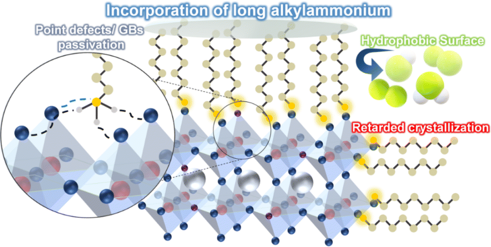 | ||
| Scheme 1 Schematic illustration of octylammonium-incorporated perovskite nanocrystals. | ||
The crystallization kinetics of perovskite films prepared with a multi-ligand system was monitored. As illustrated in Fig. 1a, the film's color transitioned from transparent to dark brown as the multi-ligand CsPbIXBr3−X films solidified and crystallized at 80 °C. The OAI-modified film exhibited a retarded nucleation rate and slower crystallization compared to the pristine film, attributed to the presence of the octylammonium ligand.38 Generally, 3D perovskite lattices rapidly self-assemble and grow in irregular phase distribution and surface defects than the quasi-2D perovskites.39 The delayed crystallization observed in the OAI-modified perovskite films suggested the formation of larger and more regular nanocrystallites in the perovskite films. To further elucidate the crystallization behavior of perovskite films, X-ray diffraction (XRD) patterns of two perovskite films, with and without OAI (2 mol%), were compared (Fig. 1b). In the pristine perovskite film, two diffraction peaks at 14.32° and 28.92° corresponding to the typical (100) and (200) planes of α-phase CsPbI3 crystals in the cubic phase were observed. Upon the introduction of OAI, the intensity of (100) and (200) diffractions for α-phase CsPbI3 crystals was enhanced, indicating that the incorporation of OAI facilitated more regulated crystal growth. Furthermore, a slight peak shift to 14.34° and 28.98° for the (100) and (200) planes, respectively, along with a narrowing of the peak width, was observed in the presence of OAI. This observation was attributed to well-dispersed mixed halides (I− and Br−) as well as a slight increase in iodide content in the perovskite films due to OAI. It is noted that the narrower diffraction peak of the perovskite film with OAI also implies enlarged nanocrystalline domains, as summarized in the ESI (Table S1†).
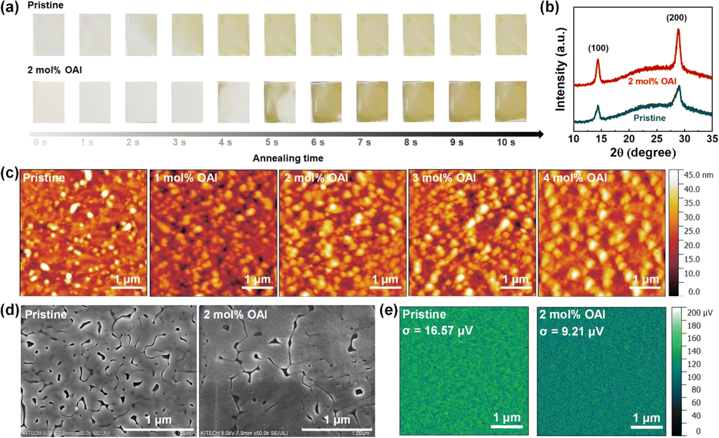 | ||
| Fig. 1 (a) Photographic images of the time-lapse of perovskite films after thermal annealing. (b) XRD characteristics, (c) AFM topographic images, (d) SEM images, and (e) KPFM images of red-emissive perovskite films with and without OAI. | ||
The surface morphologies of the perovskite films were systematically examined utilizing atomic force microscopy (AFM). As shown in Fig. 1c, the pristine perovskite film manifests discernible aggregates on a rough surface, characterized by a root-mean-squared roughness of 8.72 nm. Conversely, in the presence of OAI, the film's roughness gradually diminished, measuring 5.92, 5.31, 5.39, and 5.57 nm for films incorporated with 1, 2, 3, and 4 mol% OAI, respectively. Furthermore, the grains of the perovskite exhibited enlargement with increasing OAI content in the perovskite films, which is consistent with the XRD study. This augmentation in grain size within the perovskite crystals is attributed to the growing OAI content, presenting a notable difference in nucleation and crystal growth owing to retarded crystallization kinetics. Larger grain sizes in perovskite crystals contribute to a reduction in defective antisites, thereby elevating the probability of radiative recombination and exciton recombination energy. However, an excessive incorporation of OAI led to aggregation between crystals and the formation of very large domains within the perovskite crystals. Consequently, an optimal concentration of OAI (2 mol%) was determined to optimize the controlled crystallization kinetics of perovskite films, resulting in enlarged crystal sizes, domains, and enhanced crystallinity.
The scanning electron microscopy (SEM) images in Fig. 1d reveal a pronounced change in the film surface morphology of the OAI-modified perovskite film: uniform perovskite films with fewer pinholes were obtained by utilizing OAI as an additional ligand in the red-emitting perovskite films (Fig. S1† for lower magnification SEM images). Furthermore, Kelvin probe force microscopy (KPFM) images were collected to confirm surface potential variations in the perovskite films in Fig. 1e. The pristine perovskite films exhibited surface potential variation of σ ∼ 16.57 μV over the whole film surface, while the OAI-modified perovskite films displayed a smoother and more uniform surface potential variation throughout the film (σ ∼ 9.21 μV) (3D KPFM images and corresponding line profiles in Fig. S2†). Thus, pinhole-free, smooth perovskite films with reduced grain boundaries and defect sites could be obtained by modifying the perovskite film with OAI.40 It is also noted that the OAI-modified perovskite film exhibited increased hydrophobicity of the film surface, which also confirms partial engagement of octylammonium ligands on the lattice surface of perovskite nanocrystals and the grain boundaries of perovskite films (Fig. S3†).
Possible coordination of OAI with PbI2 is further confirmed by Fourier transform infrared spectroscopy (FT-IR). The full spectra of FT-IR of three samples are presented in Fig. S4.† In Fig. 2a, the characteristic stretching vibrations of OAI were observed in a multiple peak at ∼2900 cm−1 and a broad absorption at 3040 cm−1 for the alkyl chain (CH2/CH3) and ammonium cation (NH4+), respectively. As OAI was mixed with PbI2, the N–H absorption peak was reduced while no shift or absorption change was found in the region for C–H stretching. In the mixture of perovskite and OAI, the N–H absorption peak re-appears at a higher wavenumber of 3100 cm−1 because of Lewis acid–base chelation between Pb and ammonium ligands in the solid-state. However, multiple peaks for C–H stretching remain without peak shift. This phenomenon could be explained by sufficient coordination of ammonium in OAI with Pb2+ or Pb clusters. X-ray photoelectron spectroscopy (XPS) is then conducted to determine the electronic interaction between the perovskite and OAI (Fig. 2b). Two peaks were observed at 141.7 and 137.0 eV in the pristine perovskite film, corresponding to Pb 4f5/2 and Pb 4f7/2, respectively. Those peaks move to the higher binding energy by 0.2 eV in the OAI-modified perovskite film, implying strong coordination bonding between the perovskite and OAI. Other peaks for I 3d, Br 3d, and N 1s were also shifted to higher binding energy after OAI was incorporated in perovskite films due to enforced hydrogen bonding, which confirms the possible role in passivating the defective antisites by OAI.
 | ||
| Fig. 2 (a) FT-IR characteristics, (b) XPS binding energy spectra for Pb 4f, I 3d, Br 3d, and N 1s of perovskite films with and without OAI incorporation (2 mol%). | ||
The steady-state photoluminescence (PL) spectra for two perovskite films with varied OAI concentration are compared to examine the impact of multiligand with OAI on the optoelectronic properties of perovskite films (Fig. S5†). The pristine perovskite film, prepared from a multi-ligand system, displayed a fluorescence emission center at 643 nm with an emission width of 53.2 nm. Upon OAI addition, the PL peak exhibited a gradual hypsochromic shift to 640, 639, 637, and 634 nm for 1 to 4 mol% OAI, respectively, with a narrower emission bandwidth toward pure-red emission (Fig. 3b and Table 1). The hypsochromic shift observed in the perovskite films, resulting from the addition of OAI, can be attributed to the multifunctional role of OAI. Firstly, OAI influences the crystallization process of perovskite lattices, leading to the formation of uniform, predominantly large-grained, and defect-free perovskite films. Secondly, OAI promotes a reduction in the large-n phases and an enhancement of the small-n phases. Additionally, OAI serves to passivate defective antisites within the perovskite lattices by acting as an alkylammonium ligand. These characteristics collectively contribute to the hypsochromic shift observed in the PL spectra, indicating that the octylammonium ligand may aid in the passivation of deep- and shallow-level trap sites in perovskite nanocrystals, thereby inhibiting trap-assisted non-radiative recombination. Alongside the peak shift, a significant increase in PL intensity was observed in the OAI-modified perovskite film compared to the pristine film, as confirmed by the photographic image of the films (inset of Fig. 3a). Fig. 3c illustrates the time-resolved photoluminescence (TRPL) curves of the two perovskite films, and the raw data were fitted using a bi-exponential decay function of I = A1![[thin space (1/6-em)]](https://www.rsc.org/images/entities/char_2009.gif) exp(−t/τ1) + A2exp(−t/τ2), where A1 and A2 are relative amplitudes, and τ1 and τ2 are carrier lifetimes for fast- and slow-decay components, respectively.41 (TRPL decay curves for all samples are provided in Fig. S6† and the fitted parameters are summarized in Table S2.†) The average carrier lifetime (τavg) was calculated using the equation τavg = f1 × τ1 + f2 × τ2, where f1 and f2 are the relative ratio factors for A1 and A2 which are calculated using the equation
exp(−t/τ1) + A2exp(−t/τ2), where A1 and A2 are relative amplitudes, and τ1 and τ2 are carrier lifetimes for fast- and slow-decay components, respectively.41 (TRPL decay curves for all samples are provided in Fig. S6† and the fitted parameters are summarized in Table S2.†) The average carrier lifetime (τavg) was calculated using the equation τavg = f1 × τ1 + f2 × τ2, where f1 and f2 are the relative ratio factors for A1 and A2 which are calculated using the equation  . The fast decay component (τ1) is attributed to the defect/interface trapping process, while the slow decay component (τ2) originates from bimolecular recombination inside of the bulk perovskite film.42 The OAI-modified perovskite film exhibited an average lifetime (τavg) of 16.44 ns, which is extended compared to the pristine film (τavg = 5.15 ns). This elongated τavg suggests inhibited non-radiative recombination losses of charge carriers in the perovskite films. In addition, the relative ratio factor of fast recombination (f1) was suppressed in the presence of OAI, as summarized in Table S2.† Consequently, the fluorescence analyses conclude that the octylammonium ligand not only contributes to crystallization kinetics, leading to the formation of large crystals with high crystallinity but also influences charge carrier dynamics, suppressing defect-oriented non-radiative recombination in the red-emitting perovskite films.43
 | ||
| Fig. 3 (a) Steady-state PL spectra, (b) normalized PL spectra, (c) TRPL curves, and (d) UV-Vis absorption spectra of the perovskite films with and without OAI incorporation (2 mol%). (Inset of (a): photographic images of two perovskite films under UV irradiation; inset of (d): Urbach energy spectra of two perovskite films.) | ||
| Con. OAI (mol%) | λ EL (nm) | FWHMEL (nm) | V on (V) | ELMax (cd m−2) | EQE (%) | CIE (x, y) | LT50 (min) |
|---|---|---|---|---|---|---|---|
| N/A | 663 | 47.29 | 1.59 | 685.08 | 0.92 | (0.715, 0.284) | 348 |
| 2 | 657 | 35.50 | 1.59 | 962.15 | 8.62 | (0.711, 0.288) | 1080 |
Fig. 3d presents the absorption spectra of the two perovskite films with and without OAI. The OAI-modified film exhibited higher absorption band at lower n-phases (λ ∼ 460 and 530 nm) as compared to the pristine film, which could contribute to hypsochromic shift of emission properties. In addition, an enhanced content of 2D layered structure could provide controlled stacked layers with varied n values, which also contribute to improved film morphology.44–46 It is noteworthy that the retarded crystallization rate in the OAI-incorporated perovskite films also contributed to the preparation of improved film quality with dense grains and low defect densities. The evaluation of sub-bandgap states could be achieved by investigating the Urbach energy, reflecting lattice vibrations and defect states in polycrystalline semiconducting films. The sub-bandgap absorption near the band edge is exponentially dependent on photon energy, given by the correlation:  , where EU is the Urbach energy α(E) is the absorption coefficient of photon energy (E), and αg is the α value at the band-gap energy (Eg) with and without OAI, and the corresponding Urbach tail spectra are shown in the inset of Fig. 3d. The Urbach energy values for the pristine and OAI-modified films were 204.2 and 131.6 meV, respectively. Higher values of EU reveal substantial sub-gap Urbach tail absorption caused by defects related to halide vacancies, pinholes, or grain boundaries. Therefore, it is expected that the octylammonium ligand effectively mitigates the sub-gap defects in the perovskite films.47
To assess the impact of OAI on the optoelectronic properties of red PeLEDs, the devices with the schematic architecture of ITO-coated glass/PEDOT:PSS/perovskite/PCBM/BCP/Al were fabricated, in which, multi-ligand perovskite films were used as light-emitting layers, PEDOT:PSS and PCBM served as the hole and electron transport layers, respectively, and BCP/Al served as the cathode (Fig. 4a). Each functional layer can be clearly distinguished from the cross-sectional scanning electron microscopy (SEM) image in Fig. 4b, which reveals the clear interface of perovskite and interfacial layers. The current density (J)–voltage (V) curves and luminance (L)–V characteristics of the PeLEDs were investigated by varying the content of OAI (0, 1, 2, 3, 4 mol%) and are displayed in Fig. 4c and d. As compared to the pristine device, the OAI-modified devices exhibited distinctly reduced current level below 2 V. However, the PeLEDs showed comparable current density after the turn-on voltage (Von) (1.59 V) regardless of OAI incorporation, while the EL intensity was increased in the presence of OAI in the perovskite emitting layers. Among the varied concentrations of OAI, 2 mol% OAI exhibited the highest EL intensity, resulting in the highest current efficiency and EQE. Therefore, the optimized device configuration was set to include 2 mol% of OAI for further device analyses. When the pristine device and the target device with 2 mol% OAI are compared, much suppressed leakage current in the OAI-modified device before the turn-on voltage (Von = 1.59 V). The leakage current mainly comes from the defects of the perovskite films such as pin-holes, which reveals remarkably diminished defect density in the perovskite emitters. It is noteworthy that the trap-state density (nt) was determined by the space charge limited current (SCLC) technique from the equation nt = (VTFLεε0)/(eL2), where e is the elementary charge, L is the thickness of the perovskite absorber, ε is the dielectric constant of the perovskite film, and ε0 is the vacuum permittivity. The trap site density determined from VTFL decreased from 5.044 × 1015 cm−3 to 3.887 × 1015 cm−3 as OAI was incorporated in the perovskite films, which thus confirms that the inclusion of OAI as an additional ligand effectively eliminates the trap states and prevents the trapping of injected charge carriers (Fig. S7†).48 In the meantime, the OAI-modified PeLEDs recorded the maximum luminance of 962.15 cd m−2 which is much enhanced brightness than the control device (685.08 cd m−2) (Table 1). Notably, the lower leakage current along with excellent optical output achieved higher current efficiency (CE) and external quantum efficiency (EQE) compared to the pristine device. As a result, the PeLEDs based on pristine perovskite emitters showed relatively lower CE and EQE, while other PeLEDs based on the modified perovskite film with a 2 mol% OAI showed higher efficiency, as displayed in Fig. 4e and f (Table S3, ESI,† for device properties of all samples). The champion device of the PeLEDs with OAI incorporation exhibiting a maximum electroluminescence (ELMax) of 962.15 cd m−2 and a peak EQE of 8.62%, which outperformed the pristine device without OAI incorporation (ELMax: 685.08 cd m−2; EQE: 0.92%). In addition, the devices exhibited a high EQE level in the luminance range for 50 to 900 cd m−2 without significant EQE drop at high luminance, demonstrating the high reliability of the high quantum efficiency of the OAI-modified perovskite films in red PeLEDs.
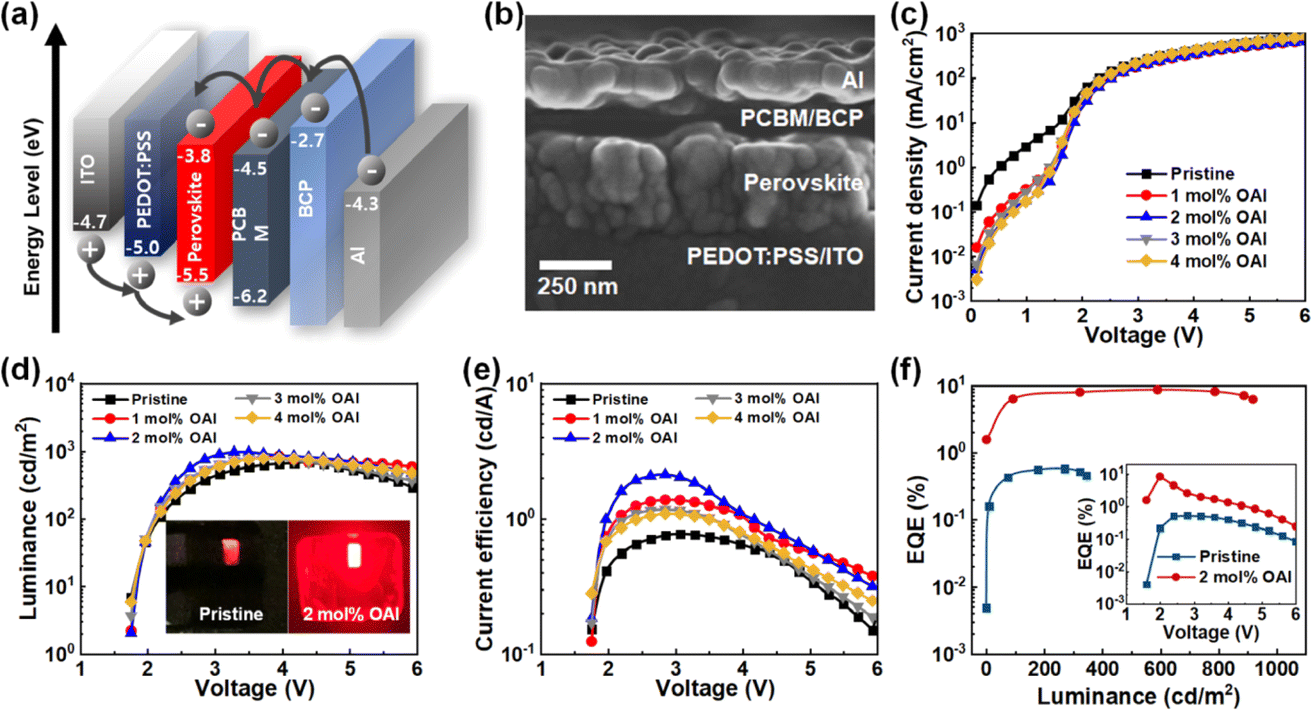 | ||
| Fig. 4 (a) Schematic illustration, (b) cross-sectional SEM image, (c) J–V curves, (d) L–V curves, (e) current efficiency curves, and (f) EQE curves of the PeLEDs with varied OAI concentration with respect to luminance. (Inset of (f): EQE curves with respect to voltage.) | ||
Fig. 5a shows the EL emission spectra of two devices, one with and one without OAI incorporation. Both devices exhibit intense emission characterized by a red color, with peak wavelength of 663 nm and 657 nm for the pristine and the target devices, respectively. It is noteworthy that the EL emission of the OAI-modified perovskite demonstrates remarkable color stability compared to the pristine device, particularly evident as the operating voltage increases from 2 to 8 V, as depicted in Fig. 5b and c. The EL emission aligns with Commission Internationale de L'Eclairage (CIE) coordinates indicative of a red color for both devices (Fig. 5c). In the pristine device, the EL emission at 663 nm corresponds to CIE coordinates (0.715, 0.284), while the addition of OAI yielded color coordinates of (0.711, 0.288) from the emission at 657 nm with a narrower bandwidth, closer to the Rec. 2020-specified primary red coordinates of (0.708, 0.292). Given that defect sites within perovskite lattices significantly influence halide ion movement under an electric field, the incorporation of OAI effectively suppresses ion migration, thereby stabilizing the band gap of the perovskite emitters. Consequently, this leads to enhanced EL stability in PeLEDs under continuous bias.49
 | ||
| Fig. 5 (a) Normalized EL emission spectra, (b) EL spectra under varied bias for the pristine device, and (c) OAI-modified device, (d) CIE coordinate, and (e) normalized EL intensity of two devices with and without OAI incorporation at an initial luminance of 100 cd m−2. | ||
Concerning the operational stability, we further investigated the lifetime performance of PeLEDs with and without OAI. Fig. 5e presents the EL lifetime data, measured at a luminance of 100 cd m−2 based on a 50% lifetime (LT50). Notably, all devices in this study were encapsulated, and measurements were performed under ambient conditions. The pristine device exhibited a lifespan of 5.8 hours, whereas the OAI-modified device demonstrated a significantly extended LT50 of 18 hours. This operational longevity, particularly at a luminance level of 100 cd m−2, is noteworthy as PeLEDs of a red emission typically struggle to attain operational lifetimes exceeding a few hours. As listed in Table S4,† the recorded lifetime in this study stands out as one of the most impressive among solution-processed state-of-the-art red PeLEDs. The observed enhancement is attributed to the reduction of trap sites facilitated by the OAI, resulting in improved film quality characterized by low leakage current and favorable charge carrier recombination. The achievement of balanced carrier transport in perovskite emitter films minimizes non-radiative recombination, thereby facilitating radiative carrier recombination and enhancing brightness.
4. Conclusions
We have demonstrated enhanced brightness, quantum efficiency, and operative stability of red PeLEDs by utilizing OAI as an additional ligand. We have systematically investigated that the incorporation of OAI retarded the crystallization kinetics of perovskite films, which enables enlarged nanocrystal domains of perovskite films with less defective sites and grain boundaries of perovskite. In addition, close interaction of octylammonium to Pb2+ was proved, leading to stabilization of the perovskite phase and defective antisites of the fluorescent perovskite films. By taking advantage of the OAI-induced improved film properties of red-emitting perovskite films, the corresponding PeLEDs achieved improved luminescence, high EQEs up to 8.62%, and CIE coordinates (0.711, 0.288), which approach the pure red Rec. 2020 specification (0.708, 0.292). The OAI modification also exhibited exceptional spectral stability and excellent operative stability of the devices for 18 h, marking a key step toward the practical applications of PeLEDs in highly reliable pure red display. This work will motivate us to incorporate long alkylammonium as additional ligands in multiligand-based perovskite emitters to prepare highly stable PeLEDs with an in-depth perspective for future work.Conflicts of interest
There are no conflicts to declare.Acknowledgements
This research was supported by the Basic Science Research Capacity Enhancement Project through Korea Basic Science Institute (National research Facilities and Equipment Center) grant funded by the Ministry of Education (Grant number: 2019R1A6C101052). This work was also supported by the Basic Science Research Program through the National Research Foundation of Korea (NRF) funded by the Ministry of Science, ICT & Future Planning (Grant number: 2020R1A6A1A03048004 and 2022R1A2C2013248).References
- Z.-K. Tan, R. S. Moghaddam, M. L. Lai, P. Docampo, R. Higler, F. Deschler, M. Price, A. Sadhanala, L. M. Pazos, D. Credgington, F. Hanusch, T. Bein, H. J. Snaith and R. H. Friend, Nat. Nanotechnol., 2014, 9(9), 687 CrossRef CAS PubMed.
- Q. A. Akkerman, G. Raino, M. V. Kovalenko and L. Manna, Nat. Mater., 2018, 17, 394 CrossRef CAS PubMed.
- X.-K. Liu, W. Xu, S. Bai, Y. Jin, J. Wang, R. H. Friend and F. Gao, Nat. Mater., 2021, 20, 10 CrossRef CAS PubMed.
- A. Fakharuddin, M. K. Gangishetty, M. Abdi-Jalebi, S.-H. Chin, A. R. bin Mohd Yusoff, D. N. Congreve, W. Tress, F. Deschler, M. Vasilopoulou and H. J. Bolink, Nat. Electron., 2022, 5, 203 CrossRef CAS.
- X. Mei, D. Jia, J. Chen, S. Zheng and X. Zhang, Nano Today, 2022, 43, 101449 CrossRef CAS.
- W. Bai, T. Xuan, H. Zhao, H. Dong, X. Cheng, L. Wang and R. J. Xie, Perovskite light-emitting diodes with an external quantum efficiency exceeding 30%, Adv. Mater., 2023, 2302283 CrossRef CAS PubMed.
- L. Protesescu, S. Yakunin, M. I. Bodnarchuk, F. Krieg, R. Caputo, C. H. Hendon, R. X. Yang, A. Walsh and M. V. Kovalenko, Nano Lett., 2015, 15, 3692 CrossRef CAS PubMed.
- B. Liu, J. Li, G. Wang, F. Ye, H. Yan, M. Zhang, S.-C. Dong, L. Lu, P. Huang, T. He, P. Xu, H.-S. Kwok and G. Li, Sci. Adv., 2022, 8, abq0138 CrossRef PubMed.
- Y. Hassan, J. H. Park, M. L. Crawford, A. Sadhanala, J. Lee, J. C. Sadighian, E. Mosconi, R. Shivanna, E. Radicchi, M. Jeong, C. Yang, H. Choi, S. H. Park, M. H. Song, F. De Angelis, C. Y. Wong, R. H. Friend, B. R. Lee and H. J. Snaith, Nature, 2021, 591, 72 CrossRef CAS PubMed.
- J. S. Kim, J.-M. Heo, G.-S. Park, S.-J. Woo, C. Cho, H. J. Yun, D.-H. Kim, J. Park, S.-C. Lee, S.-H. Park, E. Yoon, N. C. Greenham and T.-W. Lee, Nature, 2022, 611, 688 CrossRef CAS PubMed.
- J. Chen, D. Jia, R. Zhuang, Y. Hua and X. Zhang, Adv. Mater., 2022, 34, 2204259 CrossRef CAS PubMed.
- M. Liu, Q. Wan, H. Wang, F. Carulli, X. Sun, W. Zheng, L. Kong, Q. Zhang, C. Zhang, Q. Zhang, S. Brovelli and L. Li, Nat. Photonics, 2021, 15, 379 CrossRef CAS.
- Y. R. Park, H. H. Kim, S. Eom, W. K. Choi, H. Choi, B. R. Lee and Y. Kang, J. Mater. Chem. C, 2021, 9, 3608 RSC.
- Y. Hassan, O. J. Ashton, J. H. Park, G. Li, N. Sakai, B. Wenger, A.-A. Haghighirad, N. K. Noel, M. H. Song, B. R. Lee, R. H. Friend and H. J. Snaith, J. Am. Chem. Soc., 2019, 141, 1269 CrossRef CAS PubMed.
- C. Zheng, A. Liu, C. Bi and J. Tian, Acta Phys.-Chim. Sin., 2020, 37, 2007084 Search PubMed.
- H. Zhang, X. Fu, Y. Tang, H. Wang, C. Zhang, W. W. Yu, X. Wang, Y. Zhang and M. Xiao, Nat. Commun., 2019, 10, 1088 CrossRef CAS PubMed.
- D. Yang, X. Li, W. Zhou, S. Zhang, C. Meng, Y. Wu, Y. Wang and H. Zeng, CsPbBr3 Quantum Dots 2.0: Benzenesulfonic Acid Equivalent Ligand Awakens Complete Purification, Adv. Mater., 2019, 31, 1900767 CrossRef PubMed.
- J. De Roo, M. Ibanez, P. Geiregat, G. Nedelcu, W. Walravens, J. Maes, J. C. Martins, I. Van Driessche, M. V. Kovalenko and Z. Hens, ACS Nano, 2016, 10, 2071 CrossRef CAS PubMed.
- K. Lin, J. Xing, L. N. Quan, F. P. G. de Arquer, X. Gong, J. Lu, L. Xie, W. Zhao, D. Zhang, C. Yan, W. Li, X. Liu, Y. Lu, J. Kirman, E. H. Sargent, Q. Xiong and Z. Wei, Nature, 2018, 562, 245 CrossRef CAS PubMed.
- J. N. Yang, Y. Song, J. S. Yao, K. H. Wang, J. J. Wang, B. S. Zhu, M. M. Yao, S. U. Rahman, Y. F. Lan, F. J. Fan and H. B. Yao, J. Am. Chem. Soc., 2020, 142, 2956 CrossRef CAS PubMed.
- M. V. Kovalenko, L. Protesescu and M. I. Bodnarchuk, Science, 2017, 358, 745 CrossRef CAS PubMed.
- L. N. Quan, Y. Zhao, F. P. García de Arquer, R. Sabatini, G. Walters, O. Voznyy, R. Comin, Y. Li, J. Z. Fan, H. Tan, J. Pan, M. Yuan, O. M. Bakr, Z. Lu, D. H. Kim and E. H. Sargent, Nano Lett., 2017, 17, 3701 CrossRef CAS PubMed.
- L. N. Quan, B. P. Rand, R. H. Friend, S. G. Mhaisalkar, T. W. Lee and E. H. Sargent, Chem. Rev., 2019, 119, 7444 CrossRef CAS PubMed.
- W. Jiang, B. Kim and H. Chae, Opt. Lett., 2020, 45, 5800 CrossRef PubMed.
- L. Yang, Y. Zhang, J. Ma, P. Chen, Y. Yu and M. Shao, ACS Energy Lett., 2021, 6, 2386 CrossRef CAS.
- Z. Xiao, Q. Dong, C. Bi, Y. Shao and J. Huang, Adv. Mater., 2014, 26, 6503 CrossRef CAS PubMed.
- T. Salim, S. Sun, Y. Abe, A. Krishna, A. C. Grimsdalea and Y. M. Lam, J. Mater. Chem. A, 2015, 3, 8943 RSC.
- Y. F. Lan, J. S. Yao, J. N. Yang, Y. H. Song, X. C. Ru, Q. Zhang, L. Z. Feng, T. Chen, K. H. Song and H. B. Yao, Nano Lett., 2021, 21, 8756 CrossRef CAS PubMed.
- R. Parthiban, D.-H. Lim, B. Kim, S.-H. Lee, M.-H. Lee and J.-S. Lee, Chem. Commun., 2016, 52, 2067 RSC.
- Y.-K. Wang, F. Yuan, Y. Dong, J.-Y. Li, A. Johnston, B. Chen, M. I. Saidaminov, C. Zhou, X. Zheng, Y. Hou, K. Bertens, H. Ebe, D. Ma, Z. Deng, S. Yuan, R. Chen, L. K. Sagar, J. Liu, J. Fan, P. Li, X. Li, Y. Gao, M.-K. Fung, Z.-H. Lu, O. M. Bakr, L.-S. Liao and E. H. Sargent, Angew. Chem., Int. Ed., 2021, 60, 16164 CrossRef CAS PubMed.
- J. Qing, S. Ramesh, Q. Xu, X. K. Liu, H. Wang, Z. Yuan, Z. Chen, L. Hou, T. C. Sum and F. Gao, Adv. Mater., 2021, 33, 2104381 CrossRef CAS PubMed.
- J. J. Do, Y. Chung, K. S. Kim, D. H. Kim and J. W. Jung, J. Alloys Compd., 2023, 940, 168913 CrossRef.
- T. Chiba, Y. Hayashi, H. Ebe, K. Hoshi, J. Sato, S. Sato, Y.-J. Pu, S. Ohisa and J. Kido, Nat. Photonics, 2018, 12, 681 CrossRef CAS.
- Y. Chung, K. S. Kim and J. W. Jung, Chem. Eng. J., 2023, 451, 138892 CrossRef CAS.
- M. Jiang, Z. Hu, L. K. Ono and Y. Qi, Nano Res., 2021, 14, 191 CrossRef CAS.
- G. Yang, H. Zhang, S. Li, Z. Ren, G. Fang, D. Lei and G. Li, SmartMat, 2022, 3, 513 CrossRef CAS.
- Y. Zhang, L. Chouhan, E. Fron, L. Leoncino, K. Elkhouly, H. Bhatia, W. Qiu, M. B. J. Roeffaers, J. Hofkens, E. Debroye and B. Pradhan, ACS Photonics, 2023, 10, 2774 CrossRef CAS.
- X. H. Chen, H. P. Lu, K. Wang, Y. X. Zhai, V. Lunin, P. C. Sercel and M. Beard, J. Am. Chem. Soc., 2021, 143, 19438 CrossRef CAS PubMed.
- K. S. Kim, I. S. Jin, S. H. Park, S. J. Lim and J. W. Jung, ACS Appl. Mater. Interfaces, 2020, 12, 36228 CrossRef CAS PubMed.
- Y. Chung, K. S. Kim and J. W. Jung, Int. J. Energy Res., 2022, 46, 6012 CrossRef CAS.
- Y. Cai, J. Cui, M. Chen, M. Zhang, Y. Han, F. Qian, H. Zhao, S. Yang, Z. Yang, H. Bian, T. Wang, K. Guo, M. Cai, S. Dai, Z. Liu and S. Liu, Adv. Funct. Mater., 2020, 31, 2005776 CrossRef.
- Y. Zhang, Y. Li, L. Zhang, H. Hu, Z. Tang, B. Xu and N. G. Park, Adv. Energy Mater., 2021, 11, 2102538 CrossRef CAS.
- Y. S. Lee and J. W. Jung, J. Alloys Compd., 2023, 960, 171015 CrossRef CAS.
- M. Z. Tun, P. Pansa-Ngat, P. Ruankham, K. K. S. Thant, S. Kamnoedmanee, C. Seriwattanachai, W. Rueangsawang, R. Supruangnet, H. Nakajima and P. Kanjanaboos, Sci. Rep., 2023, 13, 2965 CrossRef CAS PubMed.
- N. Guan, Y. Zhang, W. Chen, Z. Jiang, L. Gu, R. Zhu, D. Yadav, D. Li, B. Xu, L. Cao, X. Gao, Y. Chen and L. Song, Adv. Sci., 2023, 10, 2205342 CrossRef CAS PubMed.
- J. J. Do, Y. Chung, K. S. Kim, D. H. Kim and J. W. Jung, J. Alloys Compd., 2023, 940, 168913 CrossRef.
- J. J. Do, J. R. Kwon, D. Kim and J. W. Jung, Dyes Pigm., 2024, 221, 111831 CrossRef CAS.
- K. S. Kim, Y. S. Lee, J. Choi and J. W. Jung, Dyes Pigm., 2023, 216, 111333 CrossRef CAS.
- F. Yuan, X. Zheng, A. Johnston, Y.-K. Wang, C. Zhou, Y. Dong, B. Chen, H. Chen, J. Z. Fan, G. Sharma, P. Li, Y. Gao, O. Voznyy, H.-T. Kung, Z.-H. Lu, O. M. Bakr and E. H. Sargent, Sci. Adv., 2020, 6, eabb0253 CrossRef CAS PubMed.
Footnotes |
| † Electronic supplementary information (ESI) available. See DOI: https://doi.org/10.1039/d4ta00369a |
| ‡ These authors contributed equally to this work. |
| This journal is © The Royal Society of Chemistry 2024 |