
 Open Access Article
 This Open Access Article is licensed under a
 Creative Commons Attribution 3.0 Unported Licence
SrTiO3 thin film photoanodes fabricated by combinatorial chemical beam vapour deposition: intricate connection between elemental composition and thin films' properties
Vincent
Rogé
 *a,
Corrado
Garlisi
a,
Petru Lunca
Popa
a,
Kevin
Menguelti
a,
Marc
Michel
a,
Christèle
Vergne
a,
Estelle
Wagner
b,
William
Maudez
b,
Giacomo
Benvenuti
b,
Bianca Rita
Pistillo
a and
Emanuele
Barborini
a
*a,
Corrado
Garlisi
a,
Petru Lunca
Popa
a,
Kevin
Menguelti
a,
Marc
Michel
a,
Christèle
Vergne
a,
Estelle
Wagner
b,
William
Maudez
b,
Giacomo
Benvenuti
b,
Bianca Rita
Pistillo
a and
Emanuele
Barborini
a
aMaterials Research and Technology (MRT) Department, Luxembourg Institute of Science and Technology (LIST), L-4422 Belvaux, Luxembourg. E-mail: vincent.roge@list.lu
b3D-Oxides, F-01630 Saint Genis Pouilly, France
First published on 15th March 2024
Abstract
In this research, we highlight an innovative combinatorial approach to explore the correlation between the elemental composition of SrTiO3 thin films and their photoelectrochemical characteristics for water splitting. Employing the Chemical Beam Vapor Deposition technique, we successfully synthesized SrxTiyOz thin films with varying Sr/Ti compositions, ranging from highly strontium cation deficient (Sr/Ti = 0.3) to rich (Sr/Ti = 2) films, in a single deposition process. A detailed examination of the near-stoichiometric range identified a narrow window wherein the crystalline perovskite structure was maintained. This enabled us to pinpoint the optimal strontium to titanium ratio composition between St/Ti = 0.8 and Sr/Ti = 1.2, resulting in the most efficient photoelectrode. The performance of these photoelectrodes was correlated with the physico–chemical properties of the SrxTiyOz films, as investigated through techniques such as X-ray diffraction, ultraviolet-visible absorption spectroscopy, X-ray photoelectron spectroscopy, and electrochemical impedance spectroscopy.
Introduction
As an eco-friendly alternative to fossil fuels, hydrogen has garnered significant interest for carbon-neutral energy applications, encompassing production, storage, and conversion. Within this framework, perovskite-based photocatalytic water splitting emerges as a pivotal process. Perovskite materials with an ABO3 structure have undergone extensive scrutiny due to their diverse physico–chemical properties, ranging from piezoelectricity and insulator–metal transition to catalytic activity and ionic conduction.1–5 Consequently, these materials find application in various fields, including memristive devices, LEDs, catalysis, solar cells, and solar water splitting.6–10Among the perovskite family, lead-free SrTiO3 stands out due to its remarkable thermal and chemical stability, and tuneable electrical properties in off-stoichiometric compositions or when doped with elements like La3+ or Nb5+.11 Additionally, its resistive switch property and indirect band gap of 3.2 eV enable ultraviolet photocatalytic activity for water treatment or hydrogen/oxygen production.12,13
Despite a decade of extensive research on SrTiO3 synthesis, understanding the structure–composition–property relations in SrTiO3 thin films remains somewhat elusive. Morgenbesser et al. noted uncertainty regarding the correlation between crystal structure, defect structure, and electrical properties of SrTiO3 thin films, especially in comparison to single crystal counterparts.14 Moreover, the deposition process strongly influences SrTiO3 thin film compositions and properties, introducing various defects.15 The study of cationic non-stoichiometry is particularly challenging during thin film growth, with implications for resulting properties. For instance, Breckenfled et al. observed an interdependence between stoichiometric deviations in SrTiO3 thin films grown by Pulsed Laser Deposition (PLD) and the laser fluence, impacting structural quality, dielectric, and thermal properties.16
While cationic off-stoichiometry in SrTiO3 films has been extensively studied for low-temperature resistive switch properties, its influence on photocatalytic or photo-electrocatalytic properties related to water splitting has received less attention.17,18 Kato et al. reported improved photocatalytic activity with excess strontium in SrTiO3 films, attributing this effect to the reduction of SrO defects acting as electron/hole recombination centers.19 Yamada et al. further corroborated this behaviour, demonstrating enhanced hydrogen production with a Sr/Ti ratio of 1.15.20 Despite providing valuable insights, these studies employed liquid-phase synthesis, limiting their applicability to the deposition of SrTiO3 continuous thin films with controlled elemental compositions. In contrast, techniques like Pulsed Laser Deposition (PLD), Molecular Beam Epitaxy (MBE), Metal Organic Vapour Phase Epitaxy (MOVPE), or Sputtering offer more advantages.15,21–25 Recently, Chemical Beam Vapour Deposition (CBVD) has been proposed for combinatorial deposition of metal oxides thin films with controlled compositions. Thanks to independent metal–organic precursors injection by an array of Knudsen effusive sources,26 CBVD turns out to be a powerful technique for the investigation of complex ternary metal oxides, as indeed perovskites. In this respect, we already demonstrated the use of CBVD for the growth of combinatorial NaTaO3 perovskite thin films, with a controlled cationic Na/Ta ratio gradient, as well as double-cation doped NaTaO3.27
In this paper, we leverage the combinatorial Chemical Beam Vapour Deposition (CBVD) approach to grow graded SrxTiyOz thin films and elucidate the relationship between composition and local physico–chemical properties, particularly photo-electrochemical performances. We discuss the interplay between cationic Sr/Ti ratios and crystalline structures, optical properties, and photo-anodic behaviours under ultraviolet light illumination. SrTiO3 films with highly strontium-deficient, stoichiometric, and highly strontium-rich regions were achieved, for the first time, in a single deposition session, revealing that optimal photoelectrochemical performances are confined to a narrow stoichiometric range of the Sr/Ti ratio.
Materials and methods
Bis(tri-isopropylcyclopentadienyl)strontium 98% (CAS 147658-82-0, Ereztech, Johns Creek, GA, USA) (Sr(iPr3Cp)2) and titanium(IV) isopropoxide 97% (CAS 546-68-9, Sigma-Aldrich, Darmstadt, Germany) (TTIP) were used as precursors for strontium and titanium respectively. The deposition of SrTiO3 thin films were performed in a Chemical Beam Vapor Deposition (CBVD) system Sybilla-450 (ABCD Technology, Nyon, Switzerland). A thorough description of an equivalent CBVD reactor is available in the work of E. Wagner et al.,26 and more details about CBVD can be found in the ref. 28. In short, this equipment allows the use substrates having size up to 450 mm diameter heated by a radiative graphite heating system up to 800 °C under molecular vacuum (<10−5 mbar). A maximum of five different precursors can be introduced simultaneously in the reactive chamber, by means of six independent injectors (for each precursor) homogeneously distributed around the substrate holder (Fig. 1a). In this work, we used a substrate holder that can fit substrates with different sizes, as presented in the Fig. 1b, including 6 substrates of 2 inches (2′′) and 7 substrates of 4 inches (4′′) (the 3 substrates of 6′′ on the picture were replaced with 4′′ ones). Single side polished (100) silicon wafer alongside with double side polished fused silica transparent wafers, both from the Siegert Wafer company (Aachen, Germany), were used as substrates. The combinatorial deposition is performed by opening one single source of titanium precursor and six sources of strontium precursor, uniformly distributed around the deposition area, to get an homogeneous Sr distribution. A highly homogeneous deposition is also possible with this equipment. In this case, all 6 sources of both titanium and strontium precursors are open. | ||
| Fig. 1 (a) Exploded schematic view of the deposition equipment representing the precursors injection aiming at the 45 cm diameters substrate. (b) Enlarged top view of the substrate holder positions respectively to the different sources (A to F) of the five precursors. Positions are labelled as 2A–B–C–D–F for 2′′ substrates, 4A–B–C–D for 4′′ substrates, and 6A–B–C for 6′′ wafers. | ||
Precursors were evaporated through Knudsen effusive sources inside the reacting chamber, at constant vapor pressure from thermostatically controlled canisters. The vapor pressure was correlated to the reservoir temperatures by Arrhenius' law. Oxygen was introduced homogeneously as a reactive gas through a dedicated gas line directly into the reacting chamber to enhance precursors decomposition and improve the growth of SrTiO3.
Film morphologies were studied by Scanning Electron Microscopy (SEM) using a Helios Nanolab 650 (FEI, Eindhoven, Netherlands), with a current of 25 pA and an acceleration voltage of 2 kV. Film thicknesses at different positions across the deposition area were estimated by Ellipsometry, using a M2000 ellipsometer (J.A. Woollam, Lincoln, USA) with the B-spline fitting model. Films crystallinity was investigated by X-Ray Diffraction (XRD) in a D8 Discover diffractometer (Brucker, Billerica, MA, USA), equipped with a Cu Kα (λ = 0.154 nm) radiation source. Diffractograms were recorded in grazing incidence mode with a X-ray radiation source angle of 0.5°, a detector scanning range from 20° to 80° with a step size of 0.02° at a scan speed of 2° s−1. Crystallites sizes were determined using the Scherrer eqn (1):
 | (1) |
 | (2) |
nλ = 2dhkl![[thin space (1/6-em)]](https://www.rsc.org/images/entities/char_2009.gif) sinθ sinθ | (3) |
Film chemical compositions and particularly the Sr/Ti element ratio across the deposition area were determined by X-ray photoelectron spectroscopy (XPS) with an Axis Ultra DLD X-ray spectrometer (Kratos Analytical, Manchester, UK). The system is equipped with a monochromatic Al Kalpha X-ray source (E = 1486.6 eV) operating at 150 W at a base pressure of around 10−9 mbar. Survey and narrow scans were acquired on an analysis area of 700 μm × 300 μm with a pass energy of 160 eV and 20 eV respectively, and binding energies were corrected for charge effects by referencing the C 1s peak at 285 eV. Prior to analyses, a 60 s-etching using a monoatomic argon gun operating at 500 V was performed to remove surface contamination.
Optical properties of films deposited on quartz substrates were investigated by Ultra-Violet/Visible/Near Infrared (UV/Vis/NIR) spectroscopy, on a LAMBDA 1050 spectrometer (PerkinElmer, Waltham, MA, USA) equipped with an integration sphere. Optical band gaps for direct allowed transition and indirect allowed transitions were investigated from the Tauc plot method, following eqn (4):
 | (4) |
 | (5) |
Photo-electrochemical and Electrochemical Impedance Spectroscopy (EIS) characterizations were achieved with a SP300 potentiostat (Biologic, Seyssinet-Pariset, France). Photo-electrochemical characterizations were carried out under UV light using a 12 W lamp at a wavelength of 365 nm.
Results and discussion
The detailed examination of the combinatorial deposition process for SrTiO3 thin films utilizing CBVD requires meticulous control over the growth parameters, specifically within the Mass Transport Limited Regime (MTLR). Ideally, achieving a Mass Transport Limited Regime (MTLR) is preferred, wherein all precursor molecules reaching the surface are seamlessly incorporated into the film. This ensures that the film composition accurately mirrors the flow composition. However, the deposition process may still be influenced by chemical reactions between precursor molecules, leading to a Chemical Reaction Limited Regime (CRLR), even at elevated substrate temperatures. In the present study, the deposition remains controlled by chemical reactions, despite the high substrate temperature.Consequently, the investigation of the combinatorial growth of SrTiO3 presented in this work involves a prior optimization of various experimental parameters, including the optimal substrate temperature, precursor partial pressures, and reaction time (not disclosed here). The determined ideal substrate temperature is 550 °C. Films deposited below 500 °C exhibit a significant amount of carbon incorporation, likely stemming from incomplete precursor decomposition. On the other hand, above 600 °C, the growth rate experiences a drastic reduction due to the rapid desorption of precursors from the surface.
The partial pressures of precursors necessary for combinatorial and homogeneous deposition were calculated following the methodology of Wagner et al.26 For a substrate temperature of 550 °C, a vapor pressure of 0.02 mbar for (Sr(iPr3Cp)2) and 0.1 mbar for TTIP were required to conduct the combinatorial study of SrxTiyOz with a graded chemical composition ranging from Sr/Ti = 0.2 to Sr/Ti = 2.0.
Fig. 2a presents a photographic depiction of the SrxTiyOz deposition conducted using the combinatorial approach. Transparent samples depict SrxTiyOz deposited on fused silica, while others show deposition on silicon wafers. Notably, concentric colour fringes are observable on silicon substrates, attributed to the radial introduction of the titanium precursor on the left side. These fringes are explained by variations in film thickness moving away from the titanium source (Fig. 2b). At 2 cm from the wafer edge near the titanium source, the film thickness is approximately 400 nm, decreasing to 250 nm at around 21 cm. Beyond this point, a threshold is evident, that can be due to the growth of a different material or to a distinct precursor decomposition kinetics. The thickness increases from 250 nm at 21 cm to almost 300 nm at the maximum distance of 39 cm. XPS analyses (Fig. 2b) performed on films at various distances from the titanium source reveal a consistent increase in the Sr/Ti content ratio from 0.2 at 2 cm to 2 at 39 cm. The stoichiometric ratio Sr/Ti = 1.0 is achieved around 19–21 cm, close to the central position of the substrate holder. The broad range of composition ratios across the entire deposition batch, from Sr/Ti = 0.2 to Sr/Ti = 2.0, provides valuable insights into understanding the growth mechanism of SrTiO3 and identifying the optimal composition for the photocatalytic oxygen evolution reaction.
 | ||
| Fig. 2 (a) Photography highlighting the colour gradient of SrxTiyOz thin films using a combinatorial deposition process at 550 °C. The deposition is performed with a uniform strontium precursor flows and a radial titanium precursor flow gradient. (b) Film thickness and Sr/Ti ratios as a function of the distance from the wafer edge close to the titanium source, determined by ellipsometry and XPS respectively. | ||
The elemental composition data presented on Fig. 3a reveal approximately 3% carbon content in titanium-rich films, a common occurrence attributed to surface contamination. However, a notable increase in carbon incorporation is observed from the stoichiometric region (Sr/Ti ratio = 1.0) to the strontium-rich region, rising from 14% to 21%. This variation can be explained by the distinct decomposition behaviour of the two utilized metal precursors. TTIP, a metal–organic precursor, contains four oxygen atoms bonded to the metal ion, facilitating the natural formation of oxidized titanium (TiOx) materials. On the other hand, Sr(iPr3Cp)2, an organometallic molecule composed of two aromatic cyclopentadiene units linked to the metallic cation, requires an external oxygen source to oxidize the cationic strontium. The high carbon content in Sr(iPr3Cp)2 also complicates the formation of carbon-free SrOx films, justifying the elevated carbon levels observed in films where the strontium precursor dominates, especially at locations distant from the titanium source.
 | ||
| Fig. 3 (a) Elemental composition and (b) element ratios Sr/Ti, O/Sr and O/Ti for Ti, Sr, O and C of SrxTiyOz films as a function of the distance from the wafer edge close to the titanium source. | ||
Within the region spanning 2 cm to 19 cm from the titanium source, an O/Ti ratio around 2, Sr/Ti ratio below 0.6 (Fig. 3b), and low carbon content in films suggest the presence of a strontium-containing titania material (Sr1−xTixO2) more than an under-stoichiometric SrTiO3. This behaviour may be attributed to the heightened reactivity of the TTIP precursor in the TTIP-rich region. A narrow window between 21 cm and 24 cm from the TTIP precursor wafer edge allows for the growth of the stoichiometric SrTiO3 phase, as evidenced by a Sr/Ti ratio close to 1.0 and O/Sr or O/Ti ratios around 3.
Beyond 24 cm from the TTIP wafer edge, Sr/Ti ratios range between 1.5 and 2.0, and O/Sr and O/Ti ratios deviate significantly from the theoretical value of 3 (Fig. 3b). The O/Ti ratio sharply increases to almost 5, while the O/Sr ratio slightly decreases to 2.5. Consequently, the strong deviation from the theoretical value of O/Sr = O/Ti = 3.0 for the perovskite SrTiO3 suggests the presence of a highly titanium deficient SrxTi1−xOy (possibly also associated SrOx or undecomposed strontium precursor) material within the film, associated with a strong carbon incorporation.
The morphologies of films at distinct positions on the substrate holder were examined through SEM and are illustrated on Fig. 4. The TiO2-rich region and the stoichiometric region exhibit identical morphologies, characterized by small grains of a few nanometers visible on the surface. Unlike film thicknesses or compositions, there is no discernible gradient between the TiO2-rich phase and the stoichiometric one. In the strontium-rich region, located far from the titanium source, the film's morphology appears rougher. While still constituting a continuous and conformal film, it displays sharp edges at the surface. Such structures are commonly associated with crystalline materials, whereas the smooth surfaces observed in the Ti-rich and stoichiometric regions are typical of amorphous materials or highly ordered structures, as found in epitaxy.
 | ||
| Fig. 4 SEM top view images of SrxTiyOz films grown at different positions over the deposition area (with the Ti source on the left from the picture). | ||
In the pursuit of comprehending the crystalline characteristics of the diverse films, we undertook XRD analyses, presenting the results on Fig. 5. Notably, films with Sr/Ti ratios below 0.8 exhibit an amorphous structure, signifying a lack of discernible crystalline order. However, as the Sr/Ti ratio reached 0.8, a significant transformation unfolded, marked by the initiation of crystallization into the cubic perovskite structure (Pm3m group, JCPDS card 35-0734) emblematic of SrTiO3. This transformative process was evidenced by the emergence of distinct (110), (200), and (211) diffraction planes at 2θ angles of 32.35°, 46.37°, and 57.74°, respectively. As the Sr/Ti ratios increased, the corresponding diffractograms exhibited pronounced, sharp diffraction peaks, a clear indication of heightened film crystallinity. Additional confirmation came from the detection of (111) and (220) diffraction planes at 2θ angles of 39.92° and 67.79°, respectively, emphasizing an improved crystalline structure.
 | ||
| Fig. 5 XRD diffractograms of SrxTiyOz thin films with different Sr/Ti ratios. | ||
The calculated degree of crystallinity, portrayed on Fig. 6a, reveals a distinctive trend. Starting at 12% for Sr/Ti = 0.8, crystallinity experiences a remarkable ascent, reaching an optimal 93% at Sr/Ti = 1.5. Subsequently, there is a minor decline to 83% at Sr/Ti = 2.0. The calculated crystallite sizes (Fig. 6b) yield a parallel pattern, with sizes ranging from 6 nm to a peak of 25 nm, followed by a modest reduction to 20 nm.
 | ||
| Fig. 6 Evolution of (a) the degree of crystallinity, (b) crystallites sizes and (c) cubic lattice constant parameters as a function of Sr/Ti ratios in films compositions. | ||
To ascertain that the obtained crystals correspond to the desired SrTiO3 cubic phase, lattice parameters have been calculated at various Sr/Ti ratios, as illustrated in Fig. 6c. From poorly crystalline films at a Sr/Ti ratio around 0.8 to those with a ratio around 1.6, the lattice constant consistently hovered around 3.908 Å, aligning with the crystalline SrTiO3 perovskite structure (JCPDS card 35-0734). However, beyond the Sr/Ti ratio of 1.6, there is a marked increase in the lattice parameter to 3.926 Å. This expansion coincides with the observed reduction in crystallinity and crystallite size beyond Sr/Ti = 1.5. The specific phase transition and the stability of different phases depend on factors such as temperature, pressure, and the Sr/Ti ratio. The Sr/Ti ratio is crucial because it affects the balance of charges in the crystal lattice. If there is an imbalance in the ratio, it can lead to changes in the arrangement of cations and influence the stability of different crystal structures.
In conjunction with XPS findings, these observations lead to the intriguing insight that a pure SrTiO3 phase cannot be formed above a strontium-to-titanium ratio of about 1.5. The diffractograms exclusively reveal the crystalline structure of SrTiO3. This suggests that, if another SrOx phase coexists, it likely assumes an amorphous form, underscoring the intricate interplay of composition and crystallinity in the synthesized films.
The optical band gap of bulk crystalline SrTiO3 is established to be approximately 3.2 eV.30 However, the optical absorption properties of films, especially the band gap, are influenced by various factors such as elemental composition, presence of defects, crystallinity, and grain sizes. Consequently, exploring the absorption properties of SrxTiyOz films, particularly deviations from the theoretical band gap, provides insights into the deviation from a pure SrTiO3 crystalline phase. Absorbance spectra covering the UV to IR regions are illustrated in Fig. 7a, revealing two distinct absorption behaviours categorized by Sr/Ti ratio.
 | ||
| Fig. 7 Optical properties of SrxTiyOz thin films for different Sr/Ti ratios: (a) optical absorbance, (b) indirect Tauc plot, (c) Urbach tail plot. | ||
For Sr/Ti ratios below 1.0, samples exhibit complete transparency to IR and visible light, initiating absorption around 325 nm. Conversely, for Sr/Ti ratios exceeding 1.0, samples start absorbing light in the visible region, with absorption increasing incrementally along with the Sr/Ti ratio. The most absorbing regions with Sr/Ti ratios above 1.8 achieve a total absorbance ranging from 20% at 800 nm to 50% at 400 nm.
Estimations of the indirect band gap energy for each SrxTiyOz region were calculated from the Tauc plot depicted in Fig. 7b, and the values are summarized in Table 1. At low Sr/Ti ratios, the indirect band gaps of the films surpass the theoretical value of 3.2 eV, registering energies above 3.50 eV. However, as the Sr/Ti ratios increase, the indirect band gap energy gradually decreases, approaching the theoretical value and reaching 3.3 eV at Sr/Ti = 1.6.
| Sr/Ti ratio | Indirect band gap (eV) | Urbach tail energy (eV) |
|---|---|---|
| 0.2 | 3.57 | — |
| 0.3 | 3.58 | — |
| 0.4 | 3.67 | 0.083 |
| 0.6 | 3.71 | 0.082 |
| 0.8 | 3.76 | — |
| 1.0 | 3.53 | 0.241 |
| 1.2 | 3.45 | 0.250 |
| 1.5 | 3.44 | 0.251 |
| 1.6 | 3.38 | 0.277 |
| 1.8 | 3.32 | 0.301 |
| 2 | 3.29 | 0.403 |
The observed trend in the indirect band gap energies suggests a nuanced relationship between the Sr/Ti ratio and the optical properties of the films. The deviation from the theoretical band gap at low Sr/Ti ratios may be attributed to factors such as variations in composition, defects, or crystal structure distortions. As the Sr/Ti ratio increases, leading to a more stoichiometric composition, the film's optical properties align more closely with the expected behaviour of SrTiO3, as evidenced by the convergence of the indirect band gap energy towards the theoretical value. This systematic analysis underscores the complex interplay of composition and structural factors in governing the optical properties of the SrxTiyOz films.
The decrease in band gap energies as the Sr/Ti ratio increases can be attributed to variations in the crystalline states of the films, as evidenced by XRD analysis. The known disparities in SrTiO3 band gap energies between single crystal and polycrystalline thin films are often linked to the presence of grain boundaries in polycrystalline structures.31,32 At these grain boundaries, atomic structures deviate from the bulk, leading to heightened concentrations of free carriers and the creation of potential barriers.31 The resulting local electric field contributes to an increase in the band gap. In our specific case, films characterized by a Sr/Ti ratio below 1.0 exhibit a predominantly amorphous nature, with small crystallites emerging at Sr/Ti = 0.8, resulting in elevated band gap energies. As the Sr/Ti ratio increases, the films exhibit improved crystallinity and larger crystallite sizes, leading to a subsequent decrease in the band gap, approaching values comparable to monocrystalline SrTiO3.
While the degree of crystallinity can account for variations in the band gap, it falls short in explaining the evolution of absorbance in the visible range for films with Sr/Ti ratios exceeding 1.0. Even in cases where the lowest gap still absorbs in the UV range, the increased absorbance in the visible range presents a conundrum.
XPS analysis reveals that films in the strontium-rich region incorporate carbon. The presence of carbon as an impurity, particularly within the lattice structure (as suggested by XRD analysis), induces structural disorder, imperfections, and defects, leading to localized absorbing states below the band gap.33 This disorder is quantified by the Urbach energy, and the calculated Urbach energies for films with varying Sr/Ti ratios are presented in Fig. 7c and Table 1. A discernible trend emerges with an increasing Sr/Ti ratio. For ratios below 1.0, the Urbach energy is negligible. However, starting from Sr/Ti = 1.0, the Urbach energy experiences a notable increase from 0.241 eV at Sr/Ti = 1.0 to 0.403 eV at Sr/Ti = 2.0. This trend affirms that as the films progress into the strontium-rich region, a greater introduction of defects occurs. This finding potentially explains the origin of visible absorption in the films, attributed to the incorporation of carbon. The systematic analysis of Urbach energies provides valuable insights into the role of defects in influencing the optical properties of the films, contributing to a more comprehensive understanding of the observed absorption behaviour.
Linear Sweep Voltammograms (LSV) conducted under ultraviolet light (365 nm) have been instrumental in assessing the photoelectrochemical performance of various Sr/Ti ratios (Fig. 8a). In the absence of light, negligible currents were recorded for all samples across the entire potential window, and films with Sr/Ti ratios below 0.6 exhibited no discernible photocurrent properties, rendering them unsuitable for electrode study. The photocurrent response of SrxTiyOz films prominently underscores the optimal photocatalytic activity achieved at the stoichiometric composition Sr/Ti = 1.0. At 2 V vs. Ag/AgCl, Sr/Ti = 1.0 displayed a photocurrent two times higher than all other compositions studied, amounting to 800 μA cm−2 compared to 400 μA cm−2. In the lower voltage range (0 V to 1.0 V), samples Sr/Ti = 0.8 and Sr/Ti = 1.0 exhibited a similar trend, with an exponential increase in photocurrent commencing at 0.2 V. However, Sr/Ti = 0.8 reached a photocurrent plateau of 400 μA cm−2 at 1.0 V, while Sr/Ti = 1.0 continued to exhibit exponential growth until 1.40 V vs. Ag/AgCl. Samples Sr/Ti = 1.2 and Sr/Ti = 0.6 commenced photocurrent production at higher voltages, around 0.8 V and 1.0 V, respectively.
 | ||
| Fig. 8 (a) Linear sweep voltammetry under UV light (365 nm) in neutral pH for different Sr/Ti ratios. (b) Photocurrent transient under chopped UV light (365 nm) at 1.23 V vs. Ag/AgCl in neutral pH for different Sr/Ti ratios. | ||
The onset potential, defined as the potential where the tangent of the photocurrent curve in the faradaic region reaches zero current (indicated by dashed lines in Fig. 8a), signifies the voltage at which photoelectrodes commence efficiency towards water oxidation or reduction. The estimated onset potentials are listed in Table 2. Notably, photoelectrodes with Sr/Ti = 0.8 exhibited the most cathodic onset potential of 0.38 V towards water oxidation. Conversely, other photoelectrodes demonstrated anodic potential shifts, with onset potentials of 0.87 V, 1.10 V, and 1.42 V for Sr/Ti = 1.0, Sr/Ti = 1.2, and Sr/Ti = 0.6, respectively. The photoelectrode with the composition Sr/Ti = 1.5 exhibited a significantly low photocurrent, precluding the estimation of the onset potential. It is crucial to acknowledge that the onset potential determined for the Sr/Ti = 1.0 photoelectrode, using the tangent to the exponential curve method, might be overestimated due to its high photocurrent production at high potential. Given the overlapping photocurrent curves below 1.0 V for Sr/Ti = 0.8 and Sr/Ti = 1.0, the onset potential of the Sr/Ti = 1.0 photoelectrode could potentially be more cathodic than calculated, at least comparable to Sr/Ti = 0.8.

| Sr/Ti | R s (Ω) | C film (nF) | R trap (Ω) | C ss (mF) | R ct,trap (Ω) |
|---|---|---|---|---|---|
| 0.6 | 398 | 2.47 | 576 | 5.73 | 3808 |
| 0.8 | 7 | 135.00 | 130 | 1.52 | 1795 |
| 1 | 26 | 102.00 | 240 | 2.35 | 390 |
| 1.2 | 24 | 55 | 385 | 1.96 | 1846 |
| 1.5 | 167 | 1.26 | 6735 | 10.01 | 38965 |
The examination of onset potentials and overall LSV curves under UV light unequivocally identifies two stoichiometric ratios, Sr/Ti = 1.0 and Sr/Ti = 0.8, as leading to efficient photoelectrodes, with optimal efficiency observed at Sr/Ti = 1.0. Fig. 8b illustrates the photocurrent generated by all photoelectrodes under chopped UV light (365 nm) in a neutral pH solution at a bias voltage of 1.23 V. All samples exhibited stable photocurrent generation throughout the studied time of 160 seconds (four steps of 20 seconds light on). Photocurrent transient values aligned with those observed by LSV at 1.23 V. Commencing with a low photocurrent of 50 μA cm−2 at Sr/Ti = 0.6, the photocurrent increased with the incorporation of strontium in the film, reaching an optimum value of 350 μA cm−2 at the stoichiometric ratio Sr/Ti = 1.0. Subsequently, a notable decrease in photocurrent was observed for strontium over-stoichiometric films, with values around 150 μA cm−2.
In elucidating the observed photoelectrochemical behaviour, our investigation focused on the interplay of surface states and charge dynamics, employing electrochemical impedance spectroscopy. Mott–Schottky analyses, conducted at varying frequencies, were integral in determining the pseudo-capacitance (Cp) and space charge capacitance (Csc) (also known as the depletion region, a region near the junction of two different semiconductor materials or regions with different doping levels) of the samples. Determining the pseudo-capacitance is crucial for the estimation of the presence of surface states, as the relation between the pseudo-capacitance and surface states capacitance (Css) is defined by the formula Css = Cplow frequency − Cphighfrequency.34 The resulting Fig. 9a and b present the pseudo-capacitances measured at 10 Hz and 10 kHz respectively, Fig. 9c present the calculated surface state capacitances and Fig. 9d the Mott–Schottky plot for different Sr/Ti ratios. Broad capacitance Css peak local maximum were notably observed in samples with Sr/Ti = 0.6 at −1.85 V and −0.45 V, Sr/Ti = 1.5 at −1.65 V and 0.65 V, and Sr/Ti = 1.2 at −1.35 V. In contrast, the stoichiometric point Sr/Ti = 1 displayed no surface state capacitance, confirming that the diminished photocatalytic performance of strontium under-stoichiometric and over-stoichiometric films can be attributed to surface defects trapping of photogenerated charge carriers. The photogenerated transient current production exhibited a consistent trend with surface states capacitance, emphasizing the prevalence of low or absent surface states in the most efficient photoelectrodes and higher surface states in amorphous or carbon-incorporating films.
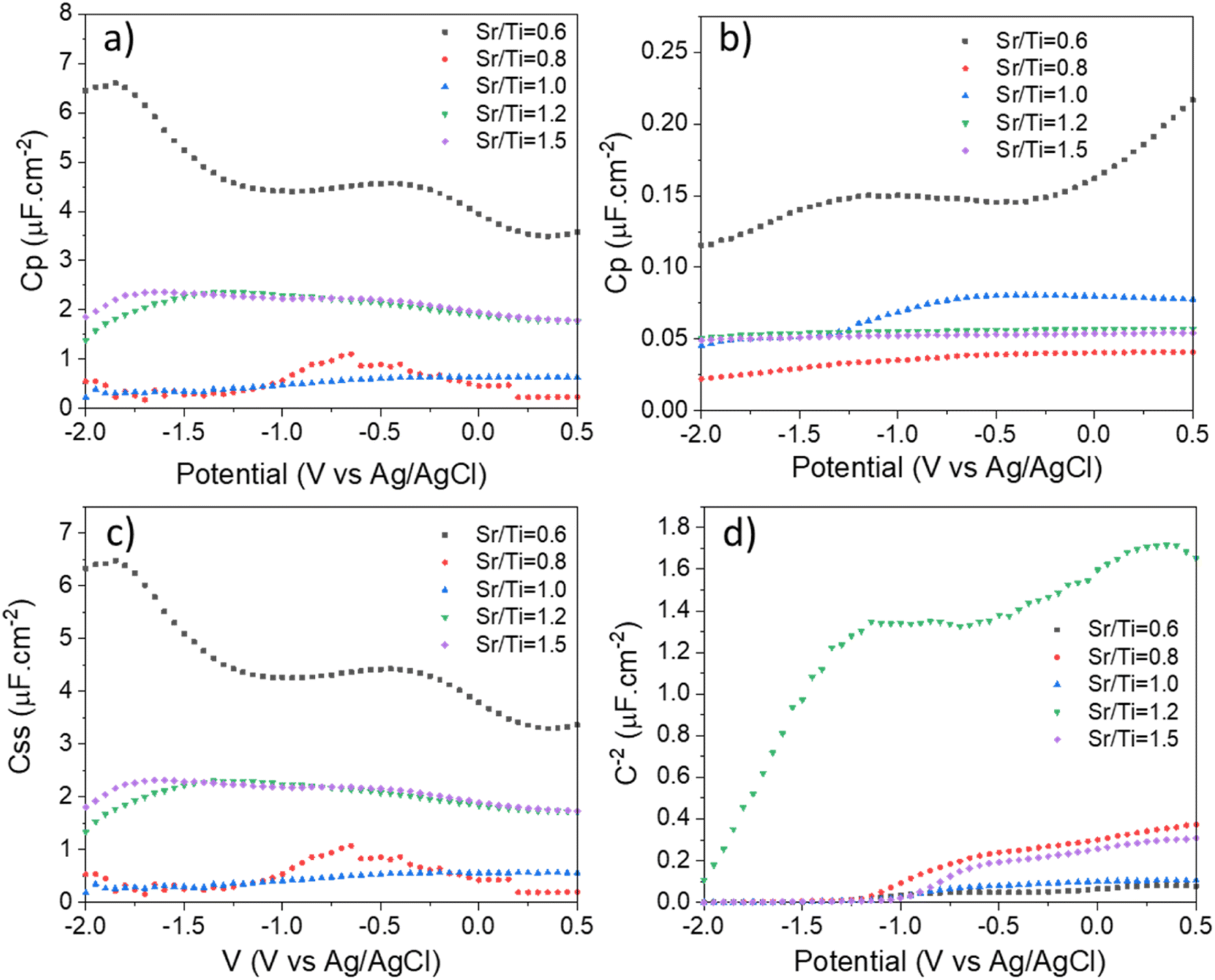 | ||
| Fig. 9 (a) Pseudo-capacitance versus potential at 10 Hz, (b) pseudo-capacitance versus potential at 10 kHz, (c) surface states capacitances calculated from pseudo-capacitances and (d) Mott–Schottky plot at 10 Hz for SrxTiyOz films with different St/Ti ratios. | ||
The complexity introduced by surface states impeded the determination of flat band potentials and carrier densities through a single high-frequency  Mott–Schottky analysis, as articulated in eqn (7):
 | (7) |
Miao et al.,35 noted the challenge of discerning the rise in differential capacitance due to the Fermi level aligning to the semiconductor band edge, especially in the presence of conduction band edge electrons trapping and detrapping with surface states near the conduction band edge. This complexity led to a non-linear Mott–Schottky characteristic, rendering a precise determination of flat band potential and carrier density unfeasible.
In light of this complexity, a pragmatic approach involved a rough estimation of flat band potential and carrier density (Nd) based on the intercept and slope, respectively, of the Mott–Schottky plot at 10 Hz, as illustrated in Fig. 9b and listed in the Table 3. The positive slope across all compositions affirmed the n-type semiconductor behaviour. Two elemental compositions, Sr/Ti = 0.8 and Sr/Ti = 1.0, stood out with concentrations of 7.52 × 10⁸ carriers per cm3 and 6.91 × 10¹⁸ carriers per cm3, respectively. Although single-frequency Mott–Schottky analysis faced reliability challenges in the presence of defects, the trend in carrier concentration aligned seamlessly with previously observed photocatalytic properties, where the most efficient photoelectrodes exhibited higher carrier densities. The apparent conduction flat band for all compositions was notably cathodic, deviating significantly from literature values36 and onset potentials observed in Linear Sweep Voltammetry (LSV). The considerable deviation between the two techniques indicated that single-frequency Mott–Schottky analysis might not be a reliable characterization technique for our samples.
| Sr/Ti | Onset potential under 365 nm irradiation (V vs. Ag/AgCl) | N d (× 1018 cm−3) | E FB (V vs. Ag/AgCl) | OCP under saturated UV light (V vs. Ag/AgCl) | OCPdark (V vs. Ag/AgCl) | Δ OCP (mV) | τ 1 (s) | τ 2 (s) | τ m (s) | Log(2τm) (s) |
|---|---|---|---|---|---|---|---|---|---|---|
| 0.6 | 1.42 | 1.18 | −1.42 | −0.227 | 0.060 | 167 | 10.42 | 131.20 | 9.65 | 1.28 |
| 0.8 | 0.38 | 7.52 | −1.87 | −0.464 | −0.050 | 415 | 22.38 | 317.47 | 20.90 | 1.62 |
| 1 | 0.87 | 6.91 | −1.71 | −0.518 | 0.058 | 576 | 13.75 | 194.01 | 12.84 | 1.41 |
| 1.2 | 1.10 | 0.50 | −2.49 | −0.382 | 0.003 | 385 | 6.77 | 173.27 | 6.51 | 1.11 |
| 1.5 | — | 0.007 | −2.06 | −0.519 | −0.048 | 471 | 20.82 | 299.68 | 19.47 | 1.59 |
To delve deeper into the mechanisms governing photocatalytic properties, charge dynamics were probed through electrochemical impedance spectroscopy at a 1.23 V bias voltage under ultraviolet light (Fig. 10a). Nyquist plots, ranging from 0.1 Hz to 100 kHz, revealed two semi-circles that could be fitted using an equivalent circuit (Fig. 10b) similar to the one found in.34 This circuit model encompassed space charge capacitance from SrxTiyOz films (Cfilm), surface state capacitance (Css), resistance from charge trapping at surface states (Rtrap), charge transfer resistance from surface states to the solution (Rct,trap), and total series resistances (Rs). Higher Cfilm values for Sr/Ti ratios of 0.8 and 1.0, compared to other compositions, affirmed the higher carrier densities observed in these samples (Table 2). The values obtained for Rct,trap shed light on the photocatalytic behaviour, particularly in the two elemental compositions (Sr/Ti = 0.8 and 1.0), which exhibited the most efficient photocatalytic activity with the lowest surface state charge transfer resistances (1795 Ω and 390 Ω, respectively). This indicated an effective surface hole collection efficiency, explaining the negative shift of the onset potential for these two elemental ratios. The lower charge transfer resistances and more cathodic onset potentials could be ascribed to more catalytically active electrodes or slower surface recombination rates.
 | ||
| Fig. 10 (a) Nyquist plot of SrxTiyOz films with different Sr/Ti ratios. (b) Equivalent electrical circuit used to fit experimental impedance parameters. | ||
To address the performance disparities among different elemental composition ratios, an Open Circuit Potential (OCP) analysis was conducted (Fig. 11). OCP, an effective method for probing the presence of trapped states and their recombination kinetics in photoactive electrodes, was utilized to quantify the transient photo-potential (Ep) in semiconductor photoanodes.37
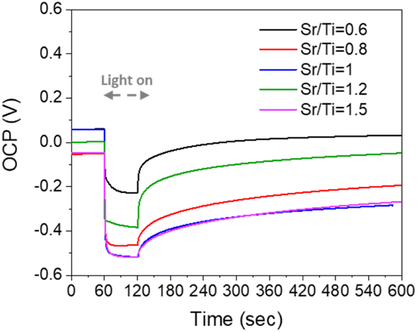 | ||
| Fig. 11 Open circuit potential (OCP) versus time decay curves measured under intense UV light and after switching off the UV light. | ||
Transient OCP versus time, recorded under intense ultraviolet light and after switching off the light, was analysed, revealing insights into the recombination kinetics of charge carriers triggered by surface trap states at the interface. The decay lifetime was obtained from fitting the OCP-t curves with a biexponential function:38
 | (8) |
 | (9) |
In the presence of illumination, all compositions of SrxTiyOz exhibit a negative photovoltage generation, signifying the injection of photogenerated electrons from SrxTiyOz films into the silicon substrate. This observation corroborates the n-type photoelectrode behaviour of SrxTiyOz films, as discerned through Mott–Schottky analysis. The disparity in Open Circuit Potential (OCP) between dark conditions and illumination (ΔOCP) serves as a direct indicator of the electronic bands' ability to bend at the photoanode/electrolyte interface following electron/hole separation. The highest ΔOCP (Table 3) value is discerned for the composition Sr/Ti = 1.0, registering at 576 mV. Subsequently, ΔOCP diminishes to 471 mV for Sr/Ti = 1.5, 415 mV for Sr/Ti = 0.8, 385 mV for Sr/Ti = 1.2, and 167 mV for Sr/Ti = 0.6. This trend underscores the enhanced effectiveness of electron/hole separation in the photoelectrode with the stoichiometric ratio Sr/Ti = 1.0, aligning with its superior photocatalytic properties.
Despite being the second-best performing composition in various electrochemical characterization techniques, akin to Sr/Ti = 1.0, Sr/Ti = 0.8 displays a smaller ΔOCP compared to Sr/Ti = 1.5 during OCP analysis. This indicates that the surface states present in Sr/Ti = 1.5 exert a relatively minimal influence on the electron/hole separation in this film. Conversely, for the composition with the highest surface states, Sr/Ti = 0.6, a notably smaller ΔOCP value of 167 mV is observed. In this scenario, the electron/hole separation is significantly compromised by the presence of surface defects. The carrier lifetimes for all compositions, as detailed in Table 3, exhibit uniformity within a range of 1.11 to 1.62 seconds. Despite the noteworthy distinctions observed in transient photocurrent production, onset potentials, carrier densities, or charge trapping resistances, the anticipated divergence in the lifetimes of photogenerated charge carriers is not evident under conditions of zero net exchange current across the semiconductor/electrolyte during transient open circuit voltage. This observation aligns with our findings for the dissimilarities in open circuit voltage decay (ΔOCV). Notably, the variations in photocatalytic activity across different elemental composition ratios manifest during redox reactions, specifically when holes react at the electrode surface. In this context, the charge transfer resistance at the interface emerges as the pivotal factor affected by surface defects.
Consequently, the conspicuously narrow photocatalytically active window centred around the stoichiometric point suggests distinct mechanisms governing the quenching of charge carriers in both under-stoichiometric and over-stoichiometric SrxTiyOz thin films. At lower strontium content, films predominantly consist of amorphous strontium-doped titania (Sr1−xTixO2) characterized by a substantial optical band gap, rendering them devoid of photocatalytic properties and incapable of absorbing 365 nm UV light. With an increase in strontium content, the formation of SrTiO3 crystallites occurs, accompanied by heightened crystallinity and Urbach energy, coupled with a reduction in band gaps. Photocatalytic properties commence to manifest and improve with the incorporation of strontium. This enhancement in crystallinity, particularly nearing the stoichiometric point Sr/Ti = 1.0, coincides with the observation of an optimum in photocatalytic activity. Subsequently, overall performance undergoes degradation. Despite the films retaining crystallinity with sizable crystallite sizes and exhibiting absorption properties at lower energies than under-stoichiometric films, an alternative mechanism, distinct from carrier recombination at boundaries, seems responsible for the decline in performance. The principal disparity between samples at Sr/Ti = 1.0 and those with Sr/Ti >1.0 lies in carbon incorporation and the excess of strontium elements in films possibly associated toa SrOx amorphous phase or undecomposed strontium precursor. The introduction of absorbing levels within the band gap due to carbon incorporation and/or strontium content appears to induce the formation of surface state defects, leading to a significant increase in transfer resistance and consequent quenching of photocatalytic activity by trapping charge carriers.
As we demonstrated that the optimal Sr/Ti ratio to obtain the most efficient photoelectrode lied between 0.8 and 1.2, we performed a homogeneous deposition at Sr/Ti = 1 on a silicon wafer covered with a platinum thin film as contact metal electrode. The measured transient photocurrent of the stoichiometric SrTiO3 thin film is presented on the Fig. 12.
 | ||
| Fig. 12 Photocurrent transient under chopped UV light (365 nm) at 1.23 V vs. Ag/AgCl in neutral pH for stoichiometric SrTiO3 deposited on Pt contact metal electrode. | ||
The photogenerated current of the film deposited on Pt contact metal shows more than a threefold improvement compared to the one deposited on silicon wafer with 1.15 mA cm−2 on platinum versus 0.350 mA cm−2 on silicon. It features the important photocatalytic performances of the grown stoichiometric SrTiO3 film when deposited on optimised electrodes.
Conclusions
The synthesis and exploration of SrxTiyOz thin films encompassing an extensive range of Sr/Ti elemental composition ratios were addressed through an innovative one-step combinatorial deposition approach utilizing Chemical Beam Vapour Deposition (CBVD). Physico-chemical properties unveiled three distinct compositional regions: the strontium under-stoichiometric region, the stoichiometric region in proximity to Sr/Ti = 1.0, and the strontium over-stoichiometric region. Although uniformity prevailed in thin films, substantial disparities emerged in terms of crystallinity, optical properties, and photoelectrochemical characteristics.Strontium under-stoichiometric films with Sr/Ti ratios below 0.8 exhibited compositions comprising amorphous Sr-incorporating TiOx phases, characterized by elevated bandgap values and conspicuously deficient photocatalytic properties. Upon the augmentation of strontium content, a crystalline cubic perovskite structure emerged, correlating with an enhancement in photocatalytic behaviour. An optimal range for photoanode performance was identified between 0.8 < Sr/Ti < 1.0. However, beyond the stoichiometric point Sr/Ti = 1.0, SrxTiyOz films maintained a highly crystalline structure. The presence of defects, attributed to a remarkable carbon content and the potential existence of a SrOx amorphous phase or undecomposed strontium precursor, hindered photocatalytic activity.
In summary, this research not only defines the optimal SrTiO3 composition for photocatalytic applications but also introduces innovative perspectives for exploring element doping. The study underscores the broader implications of combinatorial deposition in material optimization and kinetic understanding, marking a significant advancement in the field.
Author contributions
Vincent Rogé: conceptualization, methodology, formal analysis, investigation, data curation, writing—original draft preparation, review and editing. Corrado Garlisi: investigation, writing—review and editing. Kevin Menguelti: methodology, investigation. Petru Lunca-Popa: investigation, writing—review and editing. Marc Michel: investigation, writing—review and editing. Christèle Vergne: investigation, writing—review and editing. Bianca Rita Pistillo: investigation, writing—review and editing. Estelle Wagner: formal analysis, investigation, writing—review and editing. William Maudez: investigation writing—review and editing. Giacomo Benvenuti: supervision, project administration, writing—review and editing. Emanuele Barborini: conceptualization, methodology, supervision, project administration, writing—review and editing, funding acquisition.Conflicts of interest
All the authors attest that there are no conflicts to declare.Acknowledgements
XPS and XRD characterizations were carried out within the Advanced Characterization Platform of MRT department. This work is supported by the Luxembourg National Research Fund (FNR) on the Strontium Titanate Oxide with Narrow Band gap (STONB) project (BRIDGES2020/MS/14712558).References
- E. A. R. Assirey, Saudi Pharm. J., 2019, 27, 817–829 CrossRef CAS PubMed.
- A. M. Anthony, M. K. Pandian, P. Pandurangan and M. Bhagavathiachari, ACS Appl. Mater. Interfaces, 2022, 14, 29735–29743 CrossRef CAS PubMed.
- S. Halder, M. Garg, N. S. Mehta, A. Kumari, R. Sharma, T. Das, S. Chakraverty and G. Sheet, ACS Appl. Electron. Mater., 2022, 4, 5859–5866 CrossRef CAS.
- J. Hwang, R. R. Rao, L. Giordano, Y. Katayama, Y. Yu and Y. Shao-Horn, Science, 2017, 358, 751–756 CrossRef CAS PubMed.
- H. Park, C. Ha and J.-H. Lee, J. Mater. Chem. A, 2020, 8, 24353–24367 RSC.
- K. Rogdakis, M. Loizos, G. Viskadouros and E. Kymakis, Mater. Adv., 2022, 3, 7002–7014 RSC.
- J. S. Kim, J.-M. Heo, G.-S. Park, S.-J. Woo, C. Cho, H. J. Yun, D.-H. Kim, J. Park, S.-C. Lee, S.-H. Park, E. Yoon, N. C. Greenham and T.-W. Lee, Nature, 2022, 611, 688–694 CrossRef CAS PubMed.
- F. Polo-Garzon and Z. Wu, J. Mater. Chem. A, 2018, 6, 2877–2894 RSC.
- K. P. Goetz, A. D. Taylor, Y. J. Hofstetter and Y. Vaynzof, ACS Appl. Mater. Interfaces, 2021, 13, 1–17 CrossRef CAS PubMed.
- Y. Huang, J. Liu, Y. Deng, Y. Qian, X. Jia, M. Ma, C. Yang, K. Liu, Z. Wang, S. Qu and Z. Wang, J. Semicond., 2020, 41, 011701 CrossRef CAS.
- A. J. Ahmed, S. M. K. Nazrul Islam, R. Hossain, J. Kim, M. Kim, M. Billah, M. S. A. Hossain, Y. Yamauchi and X. Wang, R. Soc. Open Sci., 2019, 6, 190870 CrossRef CAS PubMed.
- T. L. Ho, K. Ding, N. Lyapunov, C. H. Suen, L. W. Wong, J. Zhao, M. Yang, X. Zhou and J. Y. Dai, Nanomaterials, 2022, 12, 2128 CrossRef CAS PubMed.
- C. Wang, H. Qiu, T. Inoue and Q. Yao, Int. J. Hydrogen Energy, 2014, 39, 12507–12514 CrossRef CAS.
- M. Morgenbesser, S. Taibl, M. Kubicek, A. Schmid, A. Viernstein, N. Bodenmüller, C. Herzig, F. Baiutti, J. de Dios Sirvent, M. O. Liedke, M. Butterling, A. Wagner, W. Artner, A. Limbeck, A. Tarancon and J. Fleig, Nanoscale Adv., 2021, 3, 6114–6127 RSC.
- P. Fisher, H. Du, M. Skowronski, P. A. Salvador, O. Maksimov and X. Weng, J. Appl. Phys., 2008, 103, 013519 CrossRef.
- E. Breckenfeld, R. Wilson, J. Karthik, A. R. Damodaran, D. G. Cahill and L. W. Martin, Chem. Mater., 2012, 24, 331–337 CrossRef CAS.
- A. Baki, J. Stöver, T. Schulz, T. Markurt, H. Amari, C. Richter, J. Martin, K. Irmscher, M. Albrecht and J. Schwarzkopf, Sci. Rep., 2021, 11, 7497 CrossRef CAS PubMed.
- M. Morgenbesser, A. Viernstein, A. Schmid, C. Herzig, M. Kubicek, S. Taibl, G. Bimashofer, J. Stahn, C. A. F. Vaz, M. Döbeli, F. Biautti, J. de Dios Sirvent, M. O. Liedke, M. Butterling, M. Kamiński, M. Tolkiehn, V. Vonk, A. Stierle, A. Wagner, A. Tarancon, A. Limbeck and J. Fleig, Adv. Funct. Mater., 2022, 32, 2202226 CrossRef CAS.
- H. Kato, Y. Sasaki, N. Shirakura and A. Kudo, J. Mater. Chem. A, 2013, 1, 12327–12333 RSC.
- K. Yamada, H. Suzuki, R. Abe and A. Saeki, J. Phys. Chem. Lett., 2019, 10, 1986–1991 CrossRef CAS PubMed.
- D. Lee, F. Liu, T. K. Truttmann, S. A. Chambers and B. Jalan, Appl. Phys. Lett., 2022, 120, 121604 CrossRef CAS.
- H. N. Lee, S. S. Ambrose Seo, W. S. Choi and C. M. Rouleau, Sci. Rep., 2016, 6, 19941 CrossRef CAS PubMed.
- R. Groenen, J. Smit, K. Orsel, A. Vailionis, B. Bastiaens, M. Huijben, K. Boller, G. Rijnders and G. Koster, APL Mater., 2015, 3, 070701 CrossRef.
- A. Baki, J. Stover, T. Schulz, T. Markurt, H. Amari, C. Richter, J. Martin, K. Irmscher, M. Albrecht and J. Schwarzkopf, Sci. Rep., 2021, 11, 7497 CrossRef CAS PubMed.
- P. Ambwani, P. Xu, G. Haugstad, J. S. Jeong, R. Deng, K. A. Mkhoyan, B. Jalan and C. Leighton, J. Appl. Phys., 2016, 120, 055704 CrossRef.
- E. Wagner, C. S. Sandu, S. Harada, C. Pellodi, M. Jobin, P. Muralt and G. Benvenuti, ACS Comb. Sci., 2016, 18, 154–161 CrossRef CAS PubMed.
- C. Garlisi, P. Lunca Popa, K. Menguelti, V. Rogé, M. Michel, C. Vergne, J. Guillot, E. Wagner, W. Maudez, G. Benvenuti, B. R. Pistillo and E. Barborini, Nanomaterials, 2022, 12, 1012 CrossRef CAS PubMed.
- E. Wagner, W. Maudez, S. Bagdzevicius, C. Sandu and G. Benvenuti, Chemical Beam Vapour Deposition Technique with Sybilla Equipment: Review of Main Results in its 20-year Anniversary, SPIE, 2021 Search PubMed.
- F. Sava, O. Diagne, A.-C. Galca, I.-D. Simandan, E. Matei, M. Burdusel, N. Becherescu, V. Becherescu, C. Mihai and A. Velea, Materials, 2020, 13, 4624 CrossRef CAS PubMed.
- D. J. Kok, K. Irmscher, M. Naumann, C. Guguschev, Z. Galazka and R. Uecker, Phys. Status Solidi A, 2015, 212, 1880–1887 CrossRef CAS.
- D. Bao, X. Yao, N. Wakiya, K. Shinozaki and N. Mizutani, Appl. Phys. Lett., 2001, 79, 3767–3769 CrossRef CAS.
- K. Xu, M. Yao, J. Chen, P. Zou, Y. Peng, F. Li and X. Yao, J. Alloys Compd., 2015, 653, 7–13 CrossRef CAS.
- N. Li and K. L. Yao, AIP Adv., 2012, 2, 032135 CrossRef.
- L. Li, H. Zhang, C. Liu, P. Liang, N. Mitsuzaki and Z. Chen, J. Mater. Sci., 2018, 54, 659–670 CrossRef.
- B. Miao, K. Sangare, A. Iqbal, B. Marsan and K. H. Bevan, Phys. Chem. Chem. Phys., 2020, 22, 19631–19642 RSC.
- A. M. Huerta-Flores, O. J. Usiobo, J. N. Audinot, R. Heyberger, P. Choquet and N. D. Boscher, ACS Appl. Mater. Interfaces, 2022, 14, 8527–8536 CrossRef CAS PubMed.
- X. Li and S. Pan, Adv. Sens. Energy Mater., 2023, 2, 100057 CrossRef.
- Y.-C. Pu, G. Wang, K.-D. Chang, Y. Ling, Y.-K. Lin, B. C. Fitzmorris, C.-M. Liu, X. Lu, Y. Tong, J. Z. Zhang, Y.-J. Hsu and Y. Li, Nano Lett., 2013, 13, 3817–3823 CrossRef CAS PubMed.
| This journal is © The Royal Society of Chemistry 2024 |