
 Open Access Article
 This Open Access Article is licensed under a
 Creative Commons Attribution 3.0 Unported Licence
Non-equilibrium defect chemistry in oxygen-rich zinc oxide nano-tetrapods synthesized using atmospheric pressure microplasma†
Dilli babu
Padmanaban
 ,
Paul
Maguire
and
Davide
Mariotti
*
,
Paul
Maguire
and
Davide
Mariotti
*
School of Engineering, Ulster University, Belfast, BT15 1AP, UK. E-mail: d.mariotti@ulster.ac.uk
First published on 19th March 2024
Abstract
We demonstrate the synthesis of zinc oxide (ZnO) nanoscale tetrapods (nTP) using an atmospheric pressure microplasma with a metal wire as a sacrificial electrode. ZnO nTPs were characterised using transmission electron microscopy (TEM), X-ray diffraction, ultraviolet-visible and photoluminescence spectroscopy. TEM clearly revealed that the nTP arm length was ∼65 nm and the diameter was around ∼11 nm, grown in the wurtzite phase along the {0001} direction containing polar surfaces. The lattice constants of the ZnO nanocrystals were evaluated using Rietveld refinement. A strong ultraviolet with weak visible-violet emission was observed though photoluminescence revealing that nTP crystals are free from intrinsic defects. Furthermore, the properties of the nTP crystals were compared with those of ZnO nanoparticles formed under different plasma conditions. A detailed formation mechanism based on optical emission spectroscopy and the crystal growth mechanism of the nTP were further discussed.
1. Introduction
Nanostructured materials are an emerging class of materials that possess unique physical and chemical properties, which have been explored and exploited for a wide range of applications including biomedical applications,1 energy,2 electronics and many more devices.3,4 Owing to their unique properties, nanoscale structures generally exhibit higher specific surface area to volume ratio, which is advantageous for effective charge collection and transport in potential optoelectronic devices.5,6 Zinc oxide (ZnO) is a transition metal oxide that showcases numerous kinds of structural features from microscopic to nanoscale regimes. Some of the common nanostructures of ZnO are zero-dimensional quantum dots,7 two-dimensional nanoplates8 or nanosheets,9 nanotubes,10 one-dimensional nanowires,11 nanorods12 and other structures.13–20ZnO is a II–VI direct wide bandgap (3.37 eV)21 semiconducting oxide with a large exciton binding energy of 60 meV. It has already been used for many potential applications such as ultraviolet (UV) laser diodes,22,23 transparent conductors,24 thin film transistors in flat panel displays,25 photoelectrodes for solar cells,26,27 piezoelectric transducers and sensors,28 dilute magnetic semiconductors and spintronics.29
ZnO can be synthesized in a variety of techniques such as the sol–gel method,30 chemical vapour deposition,31 pulsed laser deposition,32 magnetron sputtering,33 arc discharge,34 molecular beam epitaxy,35 metal organic chemical vapour deposition,36 vapour phase,37 metal organic vapour phase epitaxy38 and recently even using atmospheric pressure plasma.39–41 More specifically, plasma processes under different conditions have been also used for the synthesis of various morphologies of nanoscale ZnO (see Section 5 in the ESI† for a comparison).42–57 The synthesis of three-dimensional tetrapods was commonly reported through the thermal evaporation method58–60 in which Zn metal vapour is transported at high temperature and quenched in the presence of mainly an oxygen atmosphere to form a tetrapod structure. From a thermodynamic equilibrium perspective, the organisation of atoms into a well-organised micro or nanostructure requires macroscopic quantities such as pressure and temperature (or catalyst-activated) to reach suitable conditions that generally lead to an increase in the cost of the process.
Nano-tetrapods are special structured materials with unique forms and shapes that are different from other nanostructures like one-dimensional ZnO rods. This branched ZnO nanostructure is reported to grow by a nonadiabatic process and usually shows polytypism61i.e. existence of more than one stable ZnO crystal phase such as rods of the hexagonal wurtzite phase tetragonally connected to a central core made up of zinc blende altogether forming a stable nanostructure. The key advantage of these nano-tetrapods over standard nanorods is their geometric shape with one arm pointed normal to the substrate surface.62 They also present notable electrical, optical and mechanical properties seen as promising for photonic and nanoelectronics applications.63 Some of the well-known applications of nano-tetrapods are photocatalysis,64 photovoltaics,65 humidity sensors,60 lasers,66etc.
The ability to apply defect engineering to ZnO nTPs, especially intentional defect creation, would greatly enhance application opportunities. Defect engineering is a versatile approach used much broader in materials science and engineering with potential applications in a broader range of fields such as optoelectronics,67 energy storage,68 fuel-cell electrocatalysis,69 photovoltaics,70 nanoelectronics,71 nanozymes,72 bioimaging,73 thermoelectrics,74etc.75,76
In this report, we demonstrate the synthesis of zinc oxide nanoscale tetrapods (nTPs) via a simple setup based on atmospheric pressure plasma powered by a radio frequency (RF) source using He gas as process carrier gas. Atmospheric pressure microplasma is a versatile and cost-effective technique for the synthesis of nanomaterials77–79 offering the possibility for direct integration in application devices78 such as in solar cells.80 Here we show the formation of ZnO for different He gas and RF power and we observe the formation of nTPs for a specific parameter space. ZnO nTPs are found to be in the wurtzite phase containing polar surfaces. Further, the optical and crystalline properties were studied based on different RF power. The study will open new opportunities for the processing of nanostructured materials for microplasma in the field of optoelectronics.
2. Experimental section
ZnO nTPs were synthesized using a gas-phase atmospheric pressure microplasma (Fig. 1). A 0.5 mm diameter grounded zinc wire (99.99% purity, Goodfellow) is placed inside a quartz capillary (1 mm external, 0.7 mm internal diameters). The wire acts as the grounded electrode as well as the source of Zn for the synthesis of the ZnO nanostructures. The wire is consumed as the deposition of nanoscale ZnO progressed. Pure He gas (100% purity, grade ‘A’) is used as carrier gas at 110 sccm. The end of the quartz tube is placed through a hole of a flat copper plate which is powered by an RF (13.56 MHz, 40 W) power supply (MKSTM, Elite 300HD-01RF) through a matching unit (MFJ, MFJ VersaTuner V, Model MFJ-989 D with air-core roller inductor antenna tuner). The plasma is generated by capacitive coupling between the zinc wire and the copper plate. For comparison, experiments were also carried out under different synthesis conditions where ZnO nanoparticles of different morphologies were produced. In particular, synthesis was carried out for four different He gas flow rates 75 sccm, 110 sccm, 150 sccm and 225 sccm for fixed RF power (40 W) and three different applied power at 30 W, 40 W and 50 W with fixed He gas flow of 110 sccm. The nanocrystals are collected on a flat Si substrate and then dispersed into ethanol for further characterisation. | ||
| Fig. 1 Schematic of the microplasma setup. | ||
Plasma optical emission spectroscopy (OES) can contribute to understanding the formation mechanisms of the ZnO crystals. This technique provides information on the presence of various elemental species (Zn and O), thus helping in understanding the evolution of ZnO nTP/NPs in the microplasma. To understand the evolution of various nanoparticles plasma OES was carried out using an Ocean Optics USB 4000 spectrometer portable modular (200–1100 nm range) with a 3648-element charge couple device (CCD) array detector (Toshiba 3648-element CCD array linear image sensor). All the spectra were recorded with an integration time of 100 ms, averaged over 10 scans and corrected for electrical dark. A collimator-capped fibre optic tip was placed at two different positions (A and B, Fig. 2 with insets showing the actual microplasma emission spectra) to capture light from the plasma. The corresponding spectra were recorded from position A, representing the emission from the plasma inside the capillary (Fig. 11a) and from position B, producing spectra with emission mainly originating from the afterglow i.e. the plasma interacting with ambient air (Fig. 11b).
 | ||
| Fig. 2 Setup of optical emission measurement. | ||
UV-visible (UV-vis) absorption spectra were recorded using a Perkin Elmer-Lambda 650S UV-vis spectrometer fitted with a 150mm integrating sphere. The measurements were taken for the ZnO nTPs/ethanol colloid in a quartz cuvette of 1 cm path length. The transmittance of the colloid of nanoparticles prepared for different flow and power variations was measured. Finally, the relative absorption coefficients (α) were estimated. Thus, the bandgap of the nTP in comparison with ZnO nanoparticles prepared for different carrier flow rates and RF power was calculated using Tauc's equation.
Photoluminescence (PL) of the nanoparticle in colloid for different He gas flows and applied RF power was measured using an Agilent Cary Eclipse fluorescence spectrophotometer adjusting the excitation and emission to 10 nm, at a scan rate of 10 nm per second. The ZnO nanoparticles were dispersed in a polar solvent (ethanol, 99.5%; Sigma Aldrich) and emission from the samples was recorded for a fixed excitation wavelength (320 nm) at room temperature.
Transmission electron microscopy (TEM) and selective area electron diffraction (SAED) were carried out on a JOEL JEM-2100F accessorized with a Gatan Dual Vision 600 charge-coupled device at an accelerating voltage of 200 kV. For TEM analysis, samples are first deposited onto a Si substrate. Then the powdered samples were dispersed in ethanol (Sigma Aldrich, 99.8%) and sonicated for 10 minutes. 40 μL of samples in ethanol colloids were drop cast onto a holey carbon-coated grid (400 mesh, #S187-4, Agar Scientific) with an ultrathin carbon film (3 nm thick) and allowed to evaporate under ambient conditions overnight; d-spacing values of the crystal planes were measured on the digital image using ImageJ software.
Scanning electron microscopy (SEM) was carried out using a JOEL SEM instrument at 10 kV accelerating voltage at a working distance of 10 mm. The nanoparticles were deposited directly from the microplasma onto an ultrasonically cleaned Si (100) – n-type substrate at room temperature. Surface morphology and cross-section of the samples were recorded and further analysed using ImageJ software. Film thickness was measured by SEM analysing the sample cross section. The films were cut and mounted cross-sectionally on to an aluminium sample holder, and further microscopy imaging was performed. The thickness was evaluated at 15 different points and averaged to provide a sample thickness.
X-ray diffraction (XRD) measurements were carried out on a film of the as-deposited ZnO nanoparticles on a Si substrate using a Bruker AXS D8Discover instrument using monochromatic Cu Kα X-ray (wavelength = 1.5406 Angstroms) radiation generated at an accelerating voltage of 40 kV and current of 40 mA in glancing angle X-ray at 0.75° with respect to the sample plane. The data were acquired at a rate of 0.03 increments, and a scan speed of 12 s per step up to a total duration of 5 h. Semi-qualitative/phase quantitative analyses (Rietveld refinement) of the XRD patterns were carried out using the MAUD program.81 The theoretical pattern was generated from the standard crystal information file (cif) for Zn82 and ZnO83 obtained from the online crystallography open database.84
3. Results and discussion
3.1 Morphology and crystal structure of the ZnO nTPs
Fig. 3 shows a representative scanning electron microscopy image of ZnO nTPs deposited as a film on a Si substrate where the inset displays the film cross section. The deposit appears to be a highly porous film of interconnected ZnO nTPs with an estimated average film thickness of 10.5 ± 0.7 μm.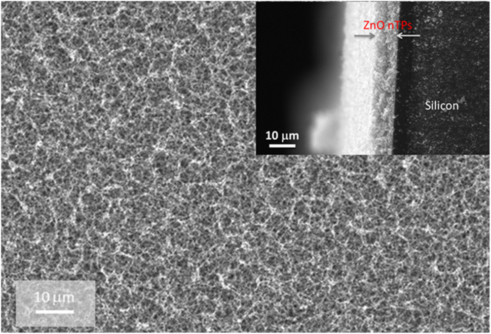 | ||
| Fig. 3 Morphology of the ZnO nTP film deposited on a Si substrate (conditions: 40 W and 110 sccm). | ||
Fig. 4a shows transmission electron micrographs (TEM) of the ZnO nTPs with the insets showing the SAED pattern and high-resolution images. For comparison, Fig. 4b and c show nanoparticles synthesized at lower (30 W) and higher (50 W) applied power, respectively. Under the selected synthesis conditions (40 W and 110 sccm, Fig. 4a), large amounts of ZnO nTPs are produced almost exclusively. The average and standard deviation of the arm length and diameter were found to be 65.6 nm ± 16.9 nm and 11.5 nm ± 2.3 nm; this was determined from the analysis of >70 nTPs. Under the other synthesis conditions (Fig. 4b and c) mixed morphologies (spherical to rectangular rod and disc-shaped nanocrystals) are observed with also minor amounts of nTPs. In Fig. 4b (30 W, 110 sccm), the majority of nanoparticles were spherical (diameter 13.8 nm ± 4.2 nm) with a few rod-like particles with the aspect (length to width) ratio ranging from 2 to 26. In Fig. 4c (50 W, 110 sccm), larger rectangular-shaped particles were observed (length scale 36.2 nm ± 13.2 nm with the aspect ratio ranging from 1 to 3); also, in this case, a small number of nTPs with much thicker arms could be found. We have also investigated the synthesis conditions corresponding to lower (75 sccm) and higher (150 sccm and 225 sccm) flow rates with respect to the synthesis conditions of the nTPs (40 W and 110 sccm, Fig. 4a); corresponding TEM images are shown in ESI, Fig. S1a–c.† The synthesis products, under the different conditions, all show a crystalline phase of hexagonal wurtzite ZnO as demonstrated by the corresponding SAED patterns (bottom right insets of Fig. 4a–c and S1a–c†).
 | ||
| Fig. 4 Transmission electron micrographs of ZnO obtained for different applied RF power (a) 40 W – nTPs, (b) 30 W and (c) 50 W at a fixed He gas flow of 110 sccm with the inset of high-resolution image and SAED pattern. | ||
Fig. 5 shows TEM images to aid a more in-depth analysis of the ZnO nTPs produced at 40 W and 110 sccm. nTPs consist of four arms at an angle of 120° with a single core of octahedral crystal.85 The nTP arms are shown in Fig. 5a–c. The fourth arm in Fig. 5d is perpendicular to the plane of the paper, mostly composed of d = 0.26 nm, i.e., the [0 0 0 2] plane shows the arms of nTPs grown along the c-axis i.e., in the {0 0 0 1} direction. A closer analysis of the arm shows hexagonal-faced crystals which indicates that these are oriented along the c-axis as represented in Fig. 5e. The d-spacing measured at the faces of the nTP arms (Fig. 5a–c) predominantly contains 0.16 nm and 0.147 nm and correspond to planes [1 1 −2 0] and [1 0 −1 3] respectively. Nevertheless, the SAED pattern on a single nTP (Fig. 5f and insets) shows dots that match to the crystal planes such as [1 0 −1 0], [0 0 0 2], [1 0 −1 3], etc. related to the dominant hexagonal phase of ZnO nTPs.
 | ||
| Fig. 5 Single ZnO nTP analysis obtained at 40 W, 110 sccm. (a–d) High-resolution transmission electron micrographs with insets of the d-spacing profile and the crystal planes of a single nTP arm. (e) Hexagonal crystal lattice of a nTP arm. (f) SAED pattern with the inset showing a single nTP particle where the yellow coloured d-spacing represents the hexagonal phase of ZnO, respectively. | ||
A highly resolved core of a nTP can be seen in Fig. 6a; here the green dotted lines represent a vertex along with orange dotted lines which depict the trigonal pyramidal part of the core crystals; a complete geometrical schematic is shown in Fig. 6b. These structures form the core of nTP crystals that have eight facets and the corresponding geometrical arrangement was successfully understood through a model proposed by Iwanaga et al.,86 called in short the “octa-twin” shown in Fig. 6c. This model suggests that the nTP core consists of eight trigonal pyramidal crystals coupled with multiple-inversion called twin crystals. Each pyramidal core crystal with four facets (Fig. 6c) constitutes a basal plane oriented along the {0 0 0 1} direction represented in blue colour and three other sides having crystal planes [1 1 −2 2], [−2 1 1 2] and [1 −2 1 2] shown in red colour respectively.60 The surface of the octahedral crystal (i.e. eight faces) has a polar face along the {0 0 0 1} direction where the four arms extend (Fig. 6b–c). The phase of this central core crystal is reported to have cubic zinc blende ZnO.87 The interface between the core structure and the hexagonal wurtzite arms is inherently linked through twinning of the crystal lattice which can be understood through the underlying symmetry as previously reported19,85 as twinned crystals are antisymmetric rather than mirror symmetric to the contact plane. However, the nTP arm from the octahedral core crystal has alternative Zn2+ {0 0 0 1} along +c and O2− {0 0 0 −1} in the −c axis. These alternative polar surfaces with counter charges are catalytically active and attract more precursor species to grow rapidly along the c-axis {0001} direction resulting in the tetrapod arm. In Fig. 6a, we also observe such a core of octa-twin crystal with geometrical face shown as dashed lines, which were represented in the completed octahedral core geometrical structure in Fig. 6b. Thus, the arms grow from the basal plane with alternating Zn and O atoms containing polar surfaces.19
 | ||
| Fig. 6 Representation of the crystal core of a ZnO nTP: (a) high-resolution micrograph of a nTP core where the fourth arm is perpendicular to the plane of the image, (b and c) geometrical representation of an octahedral core crystal. | ||
Fig. 7 shows the XRD pattern of the ZnO nTPs (40 W) and nanocrystals obtained from samples prepared for different applied RF power. All samples possess identical peaks that were indexed to the standard Joint Committee for Powder Diffraction Studies (JCPDS) file no. 65-3411, which confirms the hexagonal wurtzite phase (space group P63mc). The peak intensities are found to vary slightly depending on the synthesis conditions, where the nTPs exhibit a stronger peak corresponding to the [0 0 0 2] plane when compared to the other synthesis conditions; this is expected due to the hexagonal structure of the nTP arms (normalised peak height of about 0.69 for the nTPs at 40 W compared to 0.63 and 0.60 for 30 W and 50 W respectively). Minor peaks at 39.01° and 43.20° were identified as metallic zinc (JCPDS file no: 04-0831), indicating that the samples contain some traces of metallic zinc for lower (30 W) RF power.
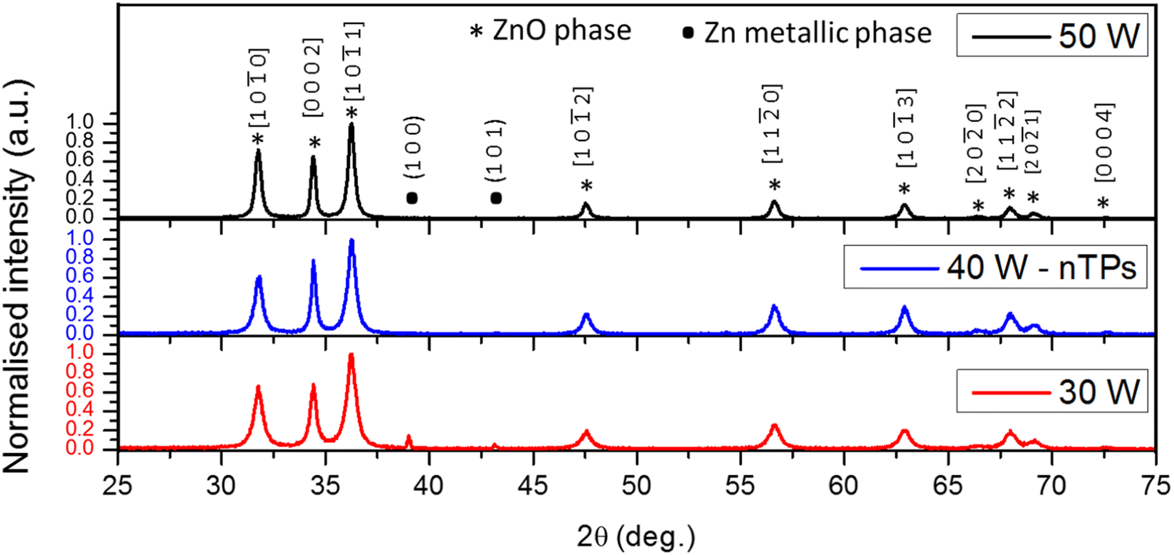 | ||
| Fig. 7 X-ray diffraction pattern of ZnO nTPs and nanocrystals for various RF power revealing various crystal planes of ZnO. | ||
Semi-quantitative analysis of the XRD peaks was carried out using Rietveld refinement with fair convergence of weighted profile R factor88 (Rwp) ∼11–12%, Rb ∼8%, and expected R factor (Rexp) ∼9%. Table 1 shows the results of this analysis which confirm the presence of metallic zinc for the samples synthesized at low power (30 W) as well as the existence of very minor metallic zinc impurities in the ZnO nTP samples prepared at 40 W.
| Applied RF power (W) | ZnO (%) | Metallic zinc (%) |
|---|---|---|
| 30 | 99.19 | 0.81 |
| 40 (nTPs) | 99.67 | 0.33 |
| 50 | 100 | 0 |
The presence of metallic zinc could be due to non-oxidized zinc particles. XRD results also provide the opportunity to study in more detail the crystal structure from where the lattice constants can be determined.89 For the hexagonal wurtzite ZnO crystal structure, experiments and first principles calculation show that the lattice constants are in the range of ‘a’ = 3.247–3.250 Å and ‘c’ = 5.204–5.207 Å respectively.90,91Fig. 8a shows the calculated lattice constants ‘a’ and ‘c’ for different applied RF power. The values are found to increase with RF power probably related to lattice expansion and increase oxide phase caused by the microplasma temperature.92 Generally any variation in thermodynamic conditions (pressure and temperature) during synthesis could change the particle size, crystallinity, nano/microstructure, etc.93 Particularly, lattice contraction is dominant in small-sized nanocrystals.94 In the case of Au and Pt metal nanoclusters, the lattice parameter varies inversely with size.95 However, for ionic metal oxide nanoparticles such as zinc oxide that possess electrostatic forces from the surface dipoles and short-range repulsive forces inside the lattice the opposite effect is more likely.96 TEM analysis shows that ZnO obtained for different powers exhibited different sizes and morphologies, particularly nTPs at 40 W. Furthermore, the change in lattice parameters can also be affected by several other reasons such as defects and crystallinity of nanoparticles. The presence of lattice defects either as foreign dopant or deficient parent atoms induces lattice strain that can contribute to the change in lattice parameters. This depends on the ionicity of parent atoms and atomic radii of dopant atoms respectively. Nanocrystals tend to show improvements in crystallinity and size with temperature97 that effectively removes lattice strains in nanocrystals thus altering the lattice parameters.91 In Fig. 8b the calculated full width at half maximum (FWHM) of the maximum intense XRD peak [1 0 −1 1] is shown to decrease with applied power. This peak broadening in terms of FWHM can be ascribed to two factors, one from nTPs/NPs and the other due to the instrument. The broadening from nanoparticles occurs from induced lattice strain due to their size, geometry, presence of defects, etc.98,99 TEM analysis shows various sizes of the ZnO structures such as 13.8 nm and 36.2 nm at 30 W and 50 W, while for nTPs, the length and diameter of the arms was 65.6 nm and 11.5 nm respectively. Thus, the presence of larger crystallites can reduce peak broadening as observed in our FWHM values along [1 0 −1 1] (Fig. 8b).
 | ||
| Fig. 8 Results from semi-quantitative analysis. (a) Variation of the lattice constant, (b) FWHM of the maximum intense peak [1 0 −1 1] and (c) ZnO unit cell condition such as aspect ratio and volume for different RF power. | ||
Fig. 8c shows the ‘c’ to ‘a’ ratio, with a value not larger than 1.604, while 1.633 is generally the expected value for hexagonal wurtzite crystals;100 however, experimental values closer to the ones we have found have been also reported.91 The value we have observed shows a dip at 40 W power, which is likely due to the presence of nTPs; Zhu et al. in their study on ZnO nanorods revealed that the lattice constant ‘c’ is found to reduce with increasing rod length.101 This is likely due to the presence of purely one-dimensional rods in the nTPs produced at 40 W. In such a case, a large number of c-axis preferentially grown nTP rods can lower the lattice constant ‘c’, hence reducing the value of the “c/a” ratio. We also observe a slight increasing trend in the unit cell volume from 30 W to 50 W (Fig. 8c) probably from the anisotropic nanocrystal growth at higher power that could increase the unit cell volume.
3.2 Optical properties
Fig. 9a shows the transmittance of ZnO nTPs/NPs synthesized at different RF applied power whereas Fig. S2a in the ESI† reveals those for variable He gas flow. All samples exhibit strong absorbance near the UV region 360–390 nm. If we assume that scattering can be considered negligible and the nature of the transition to be direct, the bandgap is estimated from Tauc's plot for different RF power and He gas flows respectively (inset Fig. 9a and S2a;† see also more generally Section 2 in the ESI†).102 In ZnO, the bandgap is determined from the hybridisation between valence orbitals of the constituents, i.e. Zn 3d and O 2p. Any change in the bond lengths (between Zn–O or O–O or Zn–Zn) from induced lattice strain will correspondingly affect the lattice constants and affect the valence electrons, which will eventually determine the band edge and bandgap. The experimental optical bandgap of ZnO has been observed to vary from 3.1 eV to 3.3 eV,103 which can be often the result of different synthesis conditions leading to somewhat different bonding arrangements. Our ZnO nanocrystals including nTPs synthesized for different RF power and He gas flows reveal the bandgap values in the range 3.22–3.26 eV as observed in Fig. 9b and S2b† respectively. The bandgap of semiconducting nanoparticles can be influenced by quantum confinement.104 Our TEM analysis (in Fig. 4 and S1†), however, has shown that the size of the nTPs and NPs is much larger than the expected ZnO Bohr exciton radius (2.87 nm).105 Thus, we do not expect quantum confinement to play a role here. Therefore, we can correlate these with the trends observed in the lattice constants and more specifically to the c/a ratio (Fig. 8c). We can observe that the bandgap in Fig. 9b follows closely the c/a ratio in Fig. 8c, i.e. a reduction of the ratio results in a larger bandgap and vice versa.106 This clearly shows that the optical properties, the bandgap in the specific case, may not depend on expansion/contraction of the crystal lattice but they might be affected by a distortion of its unit cell. | ||
| Fig. 9 Optical characteristics of ZnO nTPs and nanoparticles for different RF powers: (a) light transmittance with corresponding Tauc's plots in the inset, whereas (b) variation of the estimated bandgap observed for different applied power flows respectively. | ||
The bandgap and nature of the transition of ZnO nTPs/NPs in colloidal form obtained using Tauc plot were verified. Fig. S3a in the ESI† shows the plots corresponding to the discontinuity method where the bandgap can be extracted by fitting exponential functions. This yields a bandgap Eg of around 3.29 eV for all RF powers. The corresponding nature of the transition “r” is also determined (Fig. S3b†) and resulted in values of 0.51, 0.50 and 0.51 calculated for 30 W, 40 W and 50 W respectively. These values confirm that the ZnO nTPs/NPs obtained from microplasma synthesis exhibit a direct band transition (r = 0.5).
Fig. 10a–c show the room temperature photoluminescence emission spectra excited at 320 nm of ZnO nTPs at different applied RF power and in Fig. S4a–c† correspond to NPs produced at different He gas flows. All the samples show a strong and narrow emission peak around 385–388 nm which corresponds to the near band-to-band exciton emission; this is confirmed by its close resemblance with the bandgap calculated from absorption measurements (Fig. 9b). The luminescence spectra were analysed by decomposing them into identifiable components or bands using a Gaussian fitting model. The obtained peaks were labelled as bands Ex, v, b, g and y listed according to the emission wavelengths in Table 2 and S1.† A detailed comparison of different emission bands and defects from published sources is presented in the ESI in Table S2.† An overall energy band diagram with an emission scheme is drawn (3.36 eV bandgap) that can take place in ZnO nTPs and NPs. Under thermal equilibrium, the native point defects (Vo and Zni) predominantly exist in intrinsic zinc oxide. The formation of zinc interstitials (Zni) can be understood via Frenkel reaction at a zinc sublattice as shown in eqn (1) where VexZn and Znexi are neutral vacant and interstitial zinc sites respectively and in which the interstitial site can be further ionised to form Zni+ and Zni++ extended levels (eqn (2) and (3)) that lie further below the conduction band (CB) and Zni levels as shown in the band energy scheme (Fig. 9). Similarly, Schottky reaction (eqn (4)) can explain the formation of oxygen vacancy defect levels (Vo) as Vexo and VexZn (neutral oxygen vacancies and zinc sites) in which Vexo undergo ionisation to form Vo+ and Vo++ levels as shown in eqn (5) and (6) respectively.107
 | ||
| Fig. 10 (a–c) Photoluminescence characteristics of ZnO nTPs and nanoparticles for different RF powers, whereas (d) variation of the excitonic peak position for various synthesis conditions; and (e) emission scheme from different defect levels in ZnO nanocrystals. | ||
| RF power (W) | Interband emission, nm (eV) | Defect emission, nm (eV) | ||||
|---|---|---|---|---|---|---|
| E x | v | b | g | y | r | |
| 30 | 383.76(3.23) | 401.03(3.09) | 418.11(2.97) | 516.88(2.40) | 588.45(2.11) | — |
| 40 | 388.53(3.19) | 405.41(3.06) | 431.5(2.87) | — | — | 708.88(1.75) |
| 50 | 387.03(3.20) | 404.8(3.06) | 448.43(2.77) | — | — | 706.6(1.75) |
Frenkel reaction
| ZnZn ↔ VexZn + Znexi | (1) |
| Znexi ↔ Zni+ + e− | (2) |
| Zni+ ↔ Zni++ + e− | (3) |
Schottky reaction
| 0 ↔ Vexo + VexZn | (4) |
| Vexo ↔ Vo+ + e− | (5) |
| Vo+ ↔ Vo++ + e− | (6) |
All the spectra contain highly intense and narrow ultraviolet emission (band Ex) around 385–390 nm (∼3.2 eV) formed through recombination (interband transition) of an electron (e−) from a free exciton level near the CB to the hole (h+) in the valence band (VB). These excitonic peaks when plotted against different applied RF power show a red shift as shown in (Fig. 10d) whereas for increased He gas flows, a blue shift is found (Fig. S4†). Another shoulder peak (band v) is observed near the main UV emission located around 400 nm (∼3.01 eV), which is seen consistently in all the samples. This visible-UV emission could come either from radiative recombination of e− captured at the interstitial zinc (Zi) to h+ in the VB or due to e− from the CB that recombine with h+ at the vacant zinc site (VZn). Here the Zni is identified as a shallow donor level located 0.22 eV below the CB and it can capture an electron from the conduction band via non-radiative pathways.108–110 Likewise there is another weak shoulder at around 420 nm to 450 nm, represented as band b seen in all the samples. Zeng et. al.111 observed blue emissions (418–488 nm) arising from zinc interstitials in zinc oxide nanocrystals processed from the non-equilibrium laser ablation process and their annealing treatments. This emission is from extended or ionised zinc interstitial levels situated below the zinc interstitial levels and CB, shown in . Therefore, the blue emission band seen in ZnO nTPs and NPs can be from such ionised zinc interstitial states. In ZnO NPs obtained at 30 W and 110 sccm, 40 W and 75 sccm, and 40 W and 225 sccm a broad visible emission from 450 nm to 750 nm is observed. The spectrum is deconvoluted into green (band g) and yellow (band y) around 490–543 nm and 588–609 nm regions. Several theories have been proposed on the origin of these visible mainly green and yellow emissions and are believed to occur from single/doubly ionised oxygen vacancy (Vo) deep levels, anti-sites, oxygen interstitials, surface states, photoexcited carriers, etc.112–114 The peaks at around 490 nm can be correlated to radiative recombination of e− and h+ between one of the shallow donor zinc interstitials to an oxygen-based deep acceptor level arising from a blue shift of the green emission.111 It is also reported that green emission is also associated with oxygen-based deep acceptor states such as oxygen anti-sites (Ozn).115,116 Thus, green (band g) and yellow (band y) emission are radiative (e−–h+) recombination corresponding to the oxygen acceptor level (Voex) to the VB and the CB to Vo++.117 A weak red emission (∼705 nm) is also observed in almost all ZnO nTP and NP samples and this can be related to oxygen interstitial states (Oi). Djurišić et al. ascribed the orange-red emission (620–650 nm) to oxygen interstitials in zinc oxide nanowires and needles or to a quenching event of visible emissions to near-infrared emission close to ∼750 nm.112 Thus, oxygen-based defects act as deep levels responsible for visible emissions as observed in ZnO NPs.115,116
This analysis suggests that the nTPs are free from oxygen-based defects and instead result in a weak shoulder UV-emission from zinc interstitial or from interface trap states. However, a small excitonic peak shift as shown in Fig. 10d and S4d† for ZnO nTPs/NPs obtained for various RF power and He gas flows is observed. These shifts can be correlated with a slight change in the bandgap revealed in Fig. 9b and S2b.† Overall, the nTPs present a distorted crystal lattice responsible for a larger bandgap where the low defect density also prevents the transition from shallow states. While in part these characteristics can be attributed to the morphology of the nTPs, it is clear that the synthesis conditions at higher applied power have to be considered also responsible for producing an oxygen-rich ZnO. In order to understand this better, the process and growth mechanisms have been analysed further.
3.3 Microplasma optical emission spectroscopy
Plasma optical emission lines were identified according to the online database maintained by the National Institute of Standards and Technology-NIST.118,119Fig. 11a exhibits mostly lines originating from atomic (neutrals) and ionised state of Zn, He precursor gas and minor emission lines of N2+ band (around 425 nm). The lines from helium gas were identified at wavelengths 492 nm, 587 nm, 667 nm and 706 nm corresponding to transitions from neutral helium metastable atoms (He*).120 These emission lines are from the relaxation of various excited He* metastables to ground or intermediate states, whereby the formation of these metastables is likely through an electron impact process inside the capillary.121–123 Helium gas atoms can undergo ionisation through collision with electrons (e− + He → He+ + e−)124 to form singly ionised helium ions (He+) and their presence can be confirmed from emission at 468.6 nm in the spectra.125 In the submillimetre gap between the capillary wall and Zn wire, the energetic He+ ions can interact via a charge exchange mechanism called the Duffendack process126 that (Zn + He+ → Zn+ + He) can produce singly ionised Zn species; these were identified at 491.2 nm, 492.3 nm, 602.1 nm and 610.1 nm.127 However, He metastables also undergo Penning reactions with the Zn wire (He* + Zn → Zn+ + He + e−).128 These mechanisms were drawn based on earlier studies on dynamics of excitation and ionisation of Zn atom in He gas which were well studied in Zn/He lasers.129 | ||
| Fig. 11 Microplasma emission spectra from (a) inside the capillary tube above the exit and (b) at the exit of the capillary tube with the inset showing the actual microplasma. | ||
Excitation into helium metastables requires energies of about 19.8 eV and 20.6 eV, which are lower than the first ionisation energy (24.6 eV).130 In comparison, the ionization energies for zinc are 9.3 eV and 17.9 eV,131 respectively, which are lower than any of the He excitations above. Therefore, it is highly probable for the He metastables to produce Zn ionised species in the plasma, i.e. the formation of He metastable by electron impact is likely to be followed by ionisation of Zn rather than producing He+ ions.132 The ionised Zn+ atom can recombine with electrons (e−) aided by a third body (M), which can be either an ion or neutral atom or even with capillary walls to form excited zinc neutral species or simply Zn metastable as e− + Zn+ + M → Zn(R) + M where Zn(R) is the intermediate Rydberg state which decays radiatively to other Zn metastable levels (Zn*). This radiative decay can in fact be observed as emission lines from the capillary representing the most intense emissions at 468 nm, 472.2 nm, 481.1 nm and 636.1 nm with some minor lines at 328.7 nm, 330.8 nm and 335 nm that reflect the presence of these neutrals Zn*. Similar emission lines were reported in the case of pulsed laser deposition133 and laser ablation134 processes. Thus, the interaction of helium ions and metastables with the Zn wire supports the possibility of sputtering-producing Zn ions, which can be recombined to form Zn neutrals and can be the dominant pathways inside the capillary tube.135,136
Fig. 11b shows the emission lines recorded from the afterglow i.e. at position B (Fig. 2). Metastable-rich carrier gas along with plasma electrons and zinc neutrals interacts with ambient air constituents such as O2, N2 and H2O. The spectrum reveals a similar kind of Zn lines, which are however much lower in intensity than Zn* and Zn+ lines found from position-A emission and stronger He lines. O2 molecules are dissociated into atomic species by electron or ion or He metastables impact as predicted by chemical kinetic model simulated by Stalder et al.;137 the presence of atomic oxygen127 was seen with transitions corresponding to emission at 777 nm and 845 nm. Emission of hydrogen atomic lines Hα (656 nm),138 Hβ (486 nm)120 and the OH (307–309 nm) band can be associated with electron impact dissociation of water vapour present in air. The emission spectrum also shows stronger N2 and N2+ bands emission (391 nm and 427 nm) which may arise from the Penning ionisation of He metastables with N2 downstream of the plasma.139 This N2-related product loses energy via gas heating in the afterglow enriching the adiabatic expansion of the nanoparticles. The density of excited species in the afterglow of the plasma is strongly affected by collisions with neutral molecules in the surrounding air; for example, molecular oxygen is known to effectively quench excited  species (e.g.
 ) producing atomic oxygen species.140 Thus, near the capillary exit, the majority of excited N2 species undergo the production of atomic oxygen and can enhance the formation of ZnO nTPs/NPs by quenching.
3.4 Formation mechanism of ZnO nTPs/NPs from microplasma
In this section, we will mainly discuss the formation of nanoscale zinc oxide tetrapods in this gas phase microplasma. Optical emission results obtained from both positions clearly show that the dominant species in the gas phase are zinc and oxygen atomic neutrals. Henceforth we can consider that the formation of nTPs is from these energetic atomic neutrals present in the plasma. The Zn* species from the capillary diffuse hydrodynamically and combine with readily available atomic oxygen neutrals to form ZnO nuclei, which then grow to nTP. The formation process can be understood from the schematic represented in Fig. 12. The whole mechanism can be explained through two steps, the first represented by the formation of nuclei and the second represented by the growth of the arms into nTP. | ||
| Fig. 12 Mechanism showing the zinc oxide nanoscale tetrapod formation in the microplasma. | ||
The process of nucleation is thought to occur at the plasma exit, which is a region rich in zinc neutrals from the wire and oxygen atomic species from the atmosphere. This can be argued on the basis of similar mechanisms occurring in thermal evaporation-based tetrapod synthesis.141 In these cases, Zn atoms in the vapor exist as clusters of a small number of zinc atoms that oxidise to metastable fullerene-like structures of (ZnO)n (with n = 11, 12, 15) that further collapse to form a stable ZnO nucleus.142,143 In the microplasma (step 1, Fig. 12), the formation of zinc clusters is supplied by Zn neutrals which include metastable as well as ionized Zn, as observed by optical emission (Fig. 11). It is possible that energetic or ionized Zn atoms may impact the subsequent oxidation and formation of ZnO nuclei and therefore determine the optical properties as observed in Fig. 10. Such a process could lead to the rapid formation of nuclei in the sub-millimetre plasma region. However, the spontaneous generation of nuclei is actually related to the available free energy that depends on the saturated vapor pressure of zinc neutrals,144–147 which hinges on microplasma synthesis conditions and, for instance in the applied RF power.115
Therefore, at a given ambient oxygen concentration in the atmosphere, vapor pressure of zinc neutrals from the plasma determines the phase and rate of ZnO nucleation.61 The nuclei come together and grow as nTPs because of their interaction energy, which is identified through a potential known as Lennard–Jones potential.148 The interaction potential inversely depends on the distance between any two nuclei. In the confined microplasma, the high density of supersaturated neutrals (Zn and O) along with the ZnO nuclei lead to their growth into bigger particles. However, in the expanding plasma afterglow, since the neutrals are just energetic atoms of low mass, the growth is primarily aided by the neutrals or small mass nuclei that grow to nanostructure or larger nanoparticles as we observed for various applied RF power values.
Our TEM analysis reveals that nTPs consist of four arms with a hexagonal crystal phase, which are attached to a core crystal with eight faces and with a cubic ZnO phase. This core crystal with polar faces could actually exist as nuclei in the microplasma. Such nuclei with eight faces and cubic zinc oxide phase require high free energy for spontaneous growth to nTP.149 This energy can be supplied by the applied power and He flows gas. The presence of cubic ZnO and hexagonal arms was observed under other conditions such as with He flows at 75 sccm and 150 sccm (40 W) and at 110 sccm (50 W). However, the amount of nTPs appeared to be larger when the flow was set at 110 sccm and with the power at 40 W.
The one-dimensional hexagonal rod growth of nTPs (step 2 in Fig. 12) can be described in terms of vapour–solid (VS) mechanism. The c-axis rod growth occurs from the octahedral core crystal that consists of a polar surface oriented along the {0 0 0 1} direction. As we discussed in our TEM analysis, this surface acts as a catalytically active centre for the wurtzite rod to grow along the c-axis. Each plane perpendicular to the direction of the c-axis contains Zn2+ termination and O2− termination along the negative c-axis direction60 that attracts more monomer species. Thus, a rapid tetrapod arm growth occurs on a floating nucleus passing adiabatically in the afterglow of the plasma. The VS mechanism has also been identified for the growth of nTPs in other thermal evaporation-based techniques.150,151 The advantage of this technique is that there is no metal catalyst required, which is reported to be critical in vapor–liquid–solid methods for hierarchical nanorods growth on various substrates.152,153 In the absence of such a faceted nucleus, the growth would proceed isotropically, i.e. in all directions, resulting in spherical NPs as observed in other RF power (30 W and 50 W, 110 sccm) and flow (150 sccm and 225 sccm) conditions. Therefore, the growth of nTPs from super-saturated neutrals (Zn* and O*) and ZnO nuclei in the afterglow undergo an adiabatic expansion and result in nucleation first and growth after.
It is important to consider the role of other gaseous species present in the plasma such as energetic N2 molecules. The convective quenching during the growth of the nuclei in the afterglow with metastable species, mainly N2 gas molecules, during nTP in-flight crystal growth, determines crystallinity and its structure. To understand this, we looked at previous reports on the synthesis of ZnO using atmospheric plasma jets. Hsu et al. reported the synthesis of zinc oxide thin films using ZnCl2 as a precursor in a nitrogen-based atmospheric pressure plasma. They observed that the microstructure and crystallinity of the films improved from convective quenching of N2 metastables, while the films showed to be amorphous when oxygen was used instead of N2 gas.154 Similarly, N2 has been used in other atmospheric pressure plasma processes for enhancing the oxidation of Sn155 and in the annealing of ZnO/MgZnO films.156 Chou et al. observed lower sheet resistance in their Ga–ZnO films prepared using an atmospheric plasma jet when H2 gas was included, which was believed to cause the formation of shallow donor states in ZnO.157 Thus in our case, the crystallinity of the nTPs and NPs, as evidenced by TEM-SAED and XRD, could be due to other energetic species in the microplasma afterglow.
3.5 Effect of plasma parameters on the formation of nTPs/NPs
The synthesis conditions such as plasma power and gas flow have a decisive function in the formation of the product whether nTPs or nanoparticles (NPs). Let us first consider the effect of plasma power at a constant He flow of 110 sccm. At 30 W RF power, ∼14 nm diameter spherical particles were mainly observed, while increasing the power to 50 W beyond the nTP synthesis conditions (40 W), a few nTPs with a larger amount of particles could be produced. Likely, the main cause of these changes can be attributed to changes in vapour pressure of the zinc atomic species induced by the applied RF power for a given ambient oxygen concentration in air. For nTPs to form in the microplasma, the required pressure and temperature-inducing metastable octahedron ZnO nuclei particles are required.158 This could be also interpreted energetically considering the thermodynamic relation of the changes of free energy (ΔG) and molar enthalpy (ΔH) given as ΔG = ΔH − TΔS, where ΔS is the change in entropy and T is the absolute temperature. For a spontaneous formation of nTPs and NPs at a given applied RF power, ΔG < 0.159 The applied power generates Zn and O neutrals with some of the energy spent in heating gaseous species. There are reports on calculated molar enthalpy (ΔH) of ZnO that are found to be different based on their phase,160 size,161 and morphology.162 For example, the estimated molar enthalpy at standard temperature (298.1 K) and pressure (1 atm) for bulk ZnO is −350.46 kJ mol−1,163 nanosized (∼40 nm) zinc oxide is −322.36 kJ mol−1,164 for nanorods (∼36 nm) is −341.43 kJ mol−1.162 Therefore a slight change in the applied RF power and gas flow can easily impact the energetics leading to different sized particle and nanostructures as we observed. Nonetheless, at lower plasma power, say at 30 W and 40 W, we observe slight metallic zinc content (∼0.8–0.3%) along with nTPs/NPs. This is likely due to unoxidized Zn metal clusters. PL measurements corroborate a lower supply of reactive oxygen at low power (30 W), as a weak green emission from oxygen vacancy sites in the lattice was observed and likely originating from sub-stoichiometric reactions between excess atomic zinc and low-density oxygen neutrals in the afterglow. Metallic zinc, instead, is not observed at 50 W where all zinc clusters appear to be able to undergo full oxidation. The reason for full oxidation at higher power is likely due to a combination of factors that may include a higher gas temperature, impacting the oxidation efficiency, as well as a larger plasma that is mixing more effectively with atmosphere oxygen, hence supplying a greater amount of reactive oxygen species.When the He gas flow is changed for a fixed 40 W RF power, we observe nTP formation with flow at 110 sccm ± 40 sccm, although with irregular arms and other rod-shaped particles. Their optical properties, especially photoluminescence, show no sign of emission related to oxygen defects. However, at higher gas flows (225 sccm), the shape of NPs changes to spherical (−10 nm) with some oxygen-based defects.
The presence of oxygen defects such as oxygen anti-sites and interstitials was observed in NPs produced under two different extreme synthesis conditions such as low power (30 W) at 110 sccm and high flow (225 sccm) at 40 W. At lower applied RF power (110 sccm, 30 W), there is the possibility of incomplete crystallisation of NPs that results in an oxygen atom misplaced in a zinc site. In the case of higher gas flow (225 sccm, 40 W), the convective quenching of microplasma by He gas can lead to incomplete growth of lattice with displaced atoms as interstitials in ZnO sublattice.
Optimum conditions (40 W, 110 sccm) for a given microplasma geometry were found to produce defect-free nTP crystals that can be confirmed by photoluminescence, specifically with no oxygen vacancies and a negligible contribution to oxygen interstitials. Therefore, under these conditions, super-saturated Zn atoms from the metal wire and rapid quenching along the microplasma afterglow in the atmosphere produce nanoscale ZnO tetrapods.
4. Conclusion
Synthesis of nanoscale and intrinsic oxygen vacancy free ZnO nTPs and rich ZnO NPs was demonstrated using atmospheric pressure plasma from a zinc metal sacrificial wire as the starting material. The formation of the nTPs is closely linked to the synthesis conditions, whereby small changes in the synthesis control parameters (i.e. applied plasma power and gas flow) lead to the other ZnO morphologies with various degrees of oxygen-related defects. This demonstrates also that microplasma synthesis is a versatile approach to tune morphologies and corresponding optical properties. The nTP arms are hexagonal wurtzite grown along the (0002) plane containing polar surfaces. As the crystal growth and orientation are determined by the initial supply of Zn atoms and the plasma interface with atmospheric oxygen, the process could be tailored (e.g. controlled oxygen supply in the afterglow or even changing the reactor geometry) to favour the formation of specific morphologies, relative Zn/O concentrations or leading to diverse crystal structures. TEM, XRD, photoluminescence and XPS measurements have shown the correlation between the absence of oxygen-related defects and the optical properties. The nature of the optical transition in the crystals is confirmed to be direct with a sharp absorption transition near the UV region of the electromagnetic spectrum. The formation mechanisms have been also studied aided by thermodynamic, nucleation theories and correlated with the specific crystal and defect characteristics of the ZnO nTP. This work shows that this microplasma process can contribute to the control of oxygen-related defects in ZnO and suggests the possibility of non-equilibrium defect engineering through the manipulation of oxygen concentration for a larger family of metal oxides.Data availability
This paper is accompanied by representative samples of experimental data and the relevant numerical tabulated raw data are available from Ulster University's Research Portal at https://doi.org/10.21251/d8387316-cd6b-4ebc-be81-2bb06cc97b9b. Detailed procedures explaining how these representative samples were selected, and how these experiments can be repeated, are provided in the corresponding sections of this paper. Additional results and raw data underlying this work are available in the ESI† or on request following instructions provided at https://doi.org/10.21251/d8387316-cd6b-4ebc-be81-2bb06cc97b9b.Conflicts of interest
The authors declare no conflicts of interest.Acknowledgements
This work was supported by EPSRC (https://gow.epsrc.ukri.org/NGBOViewGrant.aspx?GrantRef=EP/V055232/1 and https://gow.epsrc.ukri.org/NGBOViewGrant.aspx?GrantRef=EP/M024938/1). We would like to thank Dr Darragh Carolan for carrying out TEM and XPS measurements.References
- H. Feyzizarnagh, D.-Y. Yoon, M. Goltz and D.-S. Kim, Peptide Nanostructures in Biomedical Technology, Wiley Interdiscip. Rev. Nanomed. Nanobiotechnol., 2016, 8(5), 730–743, DOI:10.1002/wnan.1393.
- A. L. M. Reddy and S. Ramaprabhu, Nanostructured Materials for Energy-Related Applications, in Springer Handbook of Nanomaterials, Springer Berlin Heidelberg, Berlin, Heidelberg, 2013, vol. 108, pp. 1013–1038, DOI:10.1007/978-3-642-20595-8_28.
- C. R. Martin, Nanomaterials: A Membrane-Based Synthetic Approach, Science, 1994, 266(5193), 1961–1966, DOI:10.1126/science.266.5193.1961.
- H. Gleiter, Nanostructured Materials: Basic Concepts and Microstructure, Acta Mater., 2000, 48(1), 1–29, DOI:10.1016/S1359-6454(99)00285-2.
- G. Félix and N. Thomas, Evidence of Two Effects in the Size Segregation Process in Dry Granular Media, Phys. Rev. E, 2004, 70(5), 051307, DOI:10.1103/PhysRevE.70.051307.
- P. Moriarty, Nanostructured Materials, Rep. Prog. Phys., 2001, 64(3), 297–381, DOI:10.1088/0034-4885/64/3/201.
- A. Schejn, M. Frégnaux, J. Commenge, L. Balan, L. Falk and R. Schneider, Size-Controlled Synthesis of ZnO Quantum Dots in Microreactors, Nanotechnology, 2014, 25(14), 145606–145614, DOI:10.1088/0957-4484/25/14/145606.
- S. T. Tan, A. Ali Umar and M. M. Salleh, -Faceted Hexagonal ZnO Nanoplate Thin Film Synthesis and the Heterogeneous Catalytic Reduction of 4-Nitrophenol Characterization, J. Alloys Compd., 2015, 650, 299–304, DOI:10.1016/j.jallcom.2015.06.280.
- F. Xu, M. Dai, Y. Lu and L. Sun, Hierarchical ZnO Nanowire−Nanosheet Architectures for High Power Conversion Efficiency in Dye-Sensitized Solar Cells, J. Phys. Chem. C, 2010, 114(6), 2776–2782, DOI:10.1021/jp910363w.
- Y. Sun, G. M. Fuge, N. A. Fox, D. J. Riley and M. N. R. Ashfold, Synthesis of Aligned Arrays of Ultrathin ZnO Nanotubes on a Si Wafer Coated with a Thin ZnO Film, Adv. Mater., 2005, 17(20), 2477–2481, DOI:10.1002/adma.200500726.
- Y. Wei, C. Xu, S. Xu, C. Li, W. Wu and Z. L. Wang, Planar Waveguide−Nanowire Integrated Three-Dimensional Dye-Sensitized Solar Cells, Nano Lett., 2010, 10(6), 2092–2096, DOI:10.1021/nl1005433.
- Q. X. Zhao, L. L. Yang, M. Willander, B. E. Sernelius and P. O. Holtz, Surface Recombination in ZnO Nanorods Grown by Chemical Bath Deposition, J. Appl. Phys., 2008, 104(7), 073526, DOI:10.1063/1.2991151.
- A. P. A. Oliveira, J.-F. Hochepied, F. Grillon and M.-H. Berger, Controlled Precipitation of Zinc Oxide Particles at Room Temperature, Chem. Mater., 2003, 15(16), 3202–3207, DOI:10.1021/cm0213725.
- T.-M. Shang, J.-H. Sun, Q.-F. Zhou and M.-Y. Guan, Controlled Synthesis of Various Morphologies of Nanostructured Zinc Oxide: Flower, Nanoplate, and Urchin, Cryst. Res. Technol., 2007, 42(10), 1002–1006, DOI:10.1002/crat.200710959.
- A. Kathalingam, Y. S. Chae and J. K. Rhee, Synthesis of Multi-linked ZnO Rods by Microwave Heating, Cryst. Res. Technol., 2011, 46(5), 517–522, DOI:10.1002/crat.201100097.
- A. Kathalingam and J.-K. Rhee, Hysteretic I–V Nature of Ethanol Adsorbed ZnO Nanorods, Mater. Lett., 2013, 106, 122–124, DOI:10.1016/j.matlet.2013.04.103.
- C. Y. Jiang, X. W. Sun, G. Q. Lo, D. L. Kwong and J. X. Wang, Improved Dye-Sensitized Solar Cells with a ZnO-Nanoflower Photoanode, Appl. Phys. Lett., 2007, 90(26), 263501, DOI:10.1063/1.2751588.
- X. Y. Kong and Z. L. Wang, Spontaneous Polarization-Induced Nanohelixes, Nanosprings, and Nanorings of Piezoelectric Nanobelts, Nano Lett., 2003, 3(12), 1625–1631, DOI:10.1021/nl034463p.
- Z. L. Wang, X. Y. Kong, Y. Ding, P. Gao, W. L. Hughes, R. Yang and Y. Zhang, Semiconducting and Piezoelectric Oxide Nanostructures Induced by Polar Surfaces, Adv. Funct. Mater., 2004, 14(10), 943–956, DOI:10.1002/adfm.200400180.
- Z. Zhang, H. Yuan, Y. Gao, J. Wang, D. Liu, J. Shen, L. Liu, W. Zhou, S. Xie, X. Wang, X. Zhu, Y. Zhao and L. Sun, Large-Scale Synthesis and Optical Behaviors of ZnO Tetrapods, Appl. Phys. Lett., 2007, 90(15), 153116, DOI:10.1063/1.2712512.
- A. Mang, K. Reimann and S. Rübenacke, Band Gaps, Crystal-Field Splitting, Spin-Orbit Coupling, and Exciton Binding Energies in ZnO under Hydrostatic Pressure, Solid State Commun., 1995, 94(4), 251–254, DOI:10.1016/0038-1098(95)00054-2.
- L. Dai, X. L. Chen, W. J. Wang, T. Zhou and B. Q. Hu, Growth and Luminescence Characterization of Large-Scale Zinc Oxide Nanowires, J. Condens. Matter Phys., 2003, 15(13), 2221–2226, DOI:10.1088/0953-8984/15/13/308.
- T. Ohgaki, N. Ohashi, H. Kakemoto, S. Wada, Y. Adachi, H. Haneda and T. Tsurumi, Growth Condition Dependence of Morphology and Electric Properties of ZnO Films on Sapphire Substrates Prepared by Molecular Beam Epitaxy, J. Appl. Phys., 2003, 93(4), 1961–1965, DOI:10.1063/1.1535256.
- T. L. Yang, D. H. Zhang, J. Ma, H. L. Ma and Y. Chen, Transparent Conducting ZnO:Al Films Deposited on Organic Substrates Deposited by r.f. Magnetron-Sputtering, Thin Solid Films, 1998, 326(1–2), 60–62, DOI:10.1016/S0040-6090(98)00763-9.
- B. Bayraktaroglu, K. Leedy and R. Neidhard, High Frequency ZnO Thin Film Transistors, in Device Research Conference, IEEE, 2008, vol. 85, pp. 237–238, DOI:10.1109/DRC.2008.4800819.
- G. Rey, N. Karst, B. Doisneau, H. Roussel, P. Chaudouet, V. Consonni, C. Ternon and D. Bellet, Morphological and Electrical Characterization of ZnO Nanocomposites in Dye-Sensitized Solar Cells, J. Renew. Sustain. Energy., 2011, 3(5), 059101, DOI:10.1063/1.3646762.
- N. O. V. Plank, M. E. Welland, J. L. MacManus-Driscoll and L. Schmidt-Mende, The Backing Layer Dependence of Open Circuit Voltage in ZnO/Polymer Composite Solar Cells, Thin Solid Films, 2008, 516(20), 7218–7222, DOI:10.1016/j.tsf.2007.12.037.
- A. Janotti and C. G. Van de Walle, Fundamentals of Zinc Oxide as a Semiconductor, Rep. Prog. Phys., 2009, 72(12), 126501, DOI:10.1088/0034-4885/72/12/126501.
- H. Morkoc and U. Ozgur, ZnO-Based Dilute Magnetic Semiconductors, in Zinc Oxide, Wiley-VCH Verlag GmbH & Co. KGaA, Weinheim, Germany, 2009, ch. 5, pp. 277–350, DOI:10.1002/9783527623945.
- A. J. Hashim, M. S. Jaafar, A. J. Ghazai and N. M. Ahmed, Fabrication and Characterization of ZnO Thin Film Using Sol–Gel Method, Int. J. Opt., 2013, 124(6), 491–492, DOI:10.1016/j.ijleo.2011.12.059.
- H. Sato, T. Minami, T. Miyata, S. Takata and M. Ishii, Transparent Conducting ZnO Thin Films Prepared on Low Temperature Substrates by Chemical Vapour Deposition Using Zn(C5H7O2)2, Thin Solid Films, 1994, 246(1), 65–70, DOI:10.1016/0040-6090(94)90733-1.
- F. K. Shan, G. X. Liu, Z. F. Liu, W. J. Lee, G. H. Lee, I. S. Kim, B. C. Shin and Y. S. Yu, Optical Characterizations of ZnO Thin Films on Si (100) Substrates Deposited by Pulsed Laser Deposition, J. Korean Phys. Soc., 2004, 45(DEC), S771–S775 CAS.
- T. Wallendorf, S. Marke, C. May and J. Strümpfel, Optical Investigations in a PEM Controlled Reactive Magnetron Sputter Process for Aluminium Doped Zinc Oxide Layers Using Metallic Alloy Targets, Surf. Coat. Technol., 2003, 174–175, 222–228, DOI:10.1016/S0257-8972(03)00696-0.
- E. Restrepo-Parra, L. E. Moreno-Montoya and P. J. Arango-Arango, ZnO Thin Films Growth by Pulsed Vacuum Arc Discharge, Surf. Coat. Technol., 2009, 204(3), 271–276, DOI:10.1016/j.surfcoat.2009.07.020.
- H. J. Ko, Y. F. Chen, Z. Zhu, T. Yao, I. Kobayashi and H. Uchiki, Photoluminescence Properties of ZnO Epilayers Grown on CaF2(111) by Plasma Assisted Molecular Beam Epitaxy, Appl. Phys. Lett., 2000, 76(14), 1905–1907, DOI:10.1063/1.126207.
- W. I. Park and G.-C. Yi, Photoluminescent Properties of ZnO Thin Films Grown on SiO2/Si (100) by Metal-Organic Chemical Vapor Deposition, J. Electron. Mater., 2001, 30(10), L32–L35 CrossRef CAS.
- M. Shiloh and J. Gutman, Growth of ZnO Single Crystals by Chemical Vapour Transport, J. Cryst. Growth, 1971, 11(2), 105–109, DOI:10.1016/0022-0248(71)90172-2.
- W. I. Park, Y. H. Jun, S. W. Jung and G. C. Yi, Excitonic Emissions Observed in ZnO Single Crystal Nanorods, Appl. Phys. Lett., 2003, 82(6), 964–966, DOI:10.1063/1.1544437.
- G. Jain, M. Macias-Montero, T. Velusamy, P. Maguire and D. Mariotti, Porous Zinc Oxide Nanocrystalline Film Deposition by Atmospheric Pressure Plasma: Fabrication and Energy Band Estimation, Plasma Process. Polym, 2017, 14(12), 1700052, DOI:10.1002/ppap.201700052.
- H. C. Thejaswini, B. Agasanapura and J. Hopwood, Deposition and Characterization of ZnO Films Using Microplasma at Atmospheric Pressure, Thin Solid Films, 2016, 603, 328–333, DOI:10.1016/j.tsf.2016.02.048.
- N. Bilik, B. L. Greenberg, J. Yang, E. S. Aydil and U. R. Kortshagen, Atmospheric-Pressure Glow Plasma Synthesis of Plasmonic and Photoluminescent Zinc Oxide Nanocrystals, J. Appl. Phys., 2016, 119(24), 243302, DOI:10.1063/1.4954323.
- A. S. Parlakyigit, C. Ergun and O. Gokcekaya, Synthesis of ZnO Nanoparticles via Spray Atomization Assisted Inductively Coupled Plasma Technique, Ceram. Int., 2023, 49(14), 23035–23044, DOI:10.1016/j.ceramint.2023.04.129.
- C. Zhang, X. Geng, H. Li, P.-J. He, M.-P. Planche, H. Liao, M.-G. Olivier and M. Debliquy, Microstructure and Gas Sensing Properties of Solution Precursor Plasma-Sprayed Zinc Oxide Coatings, Mater. Res. Bull., 2015, 63, 67–71, DOI:10.1016/j.materresbull.2014.11.044.
- N. Bilik, B. L. Greenberg, J. Yang, E. S. Aydil and U. R. Kortshagen, Atmospheric-Pressure Glow Plasma Synthesis of Plasmonic and Photoluminescent Zinc Oxide Nanocrystals, J. Appl. Phys., 2016, 119(24), 243302, DOI:10.1063/1.4954323.
- D. G. Tong, Y. Y. Luo, W. Chu, Y. C. Guo and W. Tian, Cutting of Carbon Nanotubes via Solution Plasma Processing, Plasma Chem. Plasma Process., 2010, 30(6), 897–905, DOI:10.1007/s11090-010-9262-3.
- A. M. Schwan, S. Chwatal, C. Hendler, D. Kopp, J. M. Lackner, R. Kaindl, M. Tscherner, M. Zirkl, P. Angerer, B. Friessnegger, S. Augl, D. Heim, A. Hinterer, M. Stummer and W. Waldhauser, Morphology-Controlled Atmospheric Pressure Plasma Synthesis of Zinc Oxide Nanoparticles for Piezoelectric Sensors, Appl. Nanosci., 2023, 13(9), 6421–6432, DOI:10.1007/s13204-023-02936-w.
- S.-C. Liao, H.-F. Lin, S.-W. Hung and C.-T. Hu, Dc Thermal Plasma Synthesis and Properties of Zinc Oxide Nanorods, J. Vac. Sci. Technol., B: Microelectron. Nanometer. Struct.–Process., Meas., Phenom., 2006, 24(3), 1322–1326, DOI:10.1116/1.2197513.
- H. Peng, Y. Fangli, B. Liuyang, L. Jinlin and C. Yunfa, Plasma Synthesis of Large Quantities of Zinc Oxide Nanorods, J. Phys. Chem. C, 2007, 111(1), 194–200, DOI:10.1021/jp065390b.
- A. Ananth, S. Dharaneedharan, H. J. Seo, M. S. Heo and J. H. Boo, Soft Jet Plasma-Assisted Synthesis of Zinc Oxide Nanomaterials: Morphology Controls and Antibacterial Activity of ZnO, Chem. Eng. J., 2017, 322, 742–751, DOI:10.1016/j.cej.2017.03.100.
- J.-S. Park and D.-W. Park, Synthesis of Zinc Oxide Nano-Particles Using Carbon Dioxide by DC Plasma Jet, Surf. Coat. Technol., 2010, 205(SUPPL. 1), S79–S83, DOI:10.1016/j.surfcoat.2010.04.046.
- D. G. Tong, P. Wu, P. K. Su, D. Q. Wang and H. Y. Tian, Preparation of Zinc Oxide Nanospheres by Solution Plasma Process and Their Optical Property, Photocatalytic and Antibacterial Activities, Mater. Lett., 2012, 70, 94–97, DOI:10.1016/j.matlet.2011.11.114.
- Y. Lin, Z. Tang, Z. Zhang, F. Yuan, Y. Ling, J. Lee and S. Huang, Preparation of Nanometer Zinc Oxide Powders by Plasma Pyrolysis Technology and Their Applications, J. Am. Ceram. Soc., 2000, 83(11), 2869–2871, DOI:10.1111/j.1151-2916.2000.tb01649.x.
- Y. Jian-Feng, L. You-Ming, L. Hong-Wei, L. Yi-Chun, L. Bing-Hui, F. Xi-Wu and Z. Jun-Ming, Growth and Properties of ZnO Nanotubes Grown on Si(111) Substrate by Plasma-Assisted Molecular Beam Epitaxy, J. Cryst. Growth, 2005, 280(1–2), 206–211, DOI:10.1016/j.jcrysgro.2005.03.045.
- D. Barreca, D. Bekermann, E. Comini, A. Devi, R. A. Fischer, A. Gasparotto, C. Maccato, G. Sberveglieri and E. Tondello, 1D ZnO Nano-Assemblies by Plasma-CVD as Chemical Sensors for Flammable and Toxic Gases, Sens. Actuators, B, 2010, 149(1), 1–7, DOI:10.1016/j.snb.2010.06.048.
- X.-H. Zhang, S.-Y. Xie, Z.-Y. Jiang, X. Zhang, Z.-Q. Tian, Z.-X. Xie, R.-B. Huang and L.-S. Zheng, Rational Design and Fabrication of ZnO Nanotubes from Nanowire Templates in a Microwave Plasma System, J. Phys. Chem. B, 2003, 107(37), 10114–10118, DOI:10.1021/jp034487k.
- J. D. Pedersen, H. J. Esposito and K. S. Teh, Direct Synthesis and Characterization of Optically Transparent Conformal Zinc Oxide Nanocrystalline Thin Films by Rapid Thermal Plasma CVD, Nanoscale Res. Lett., 2011, 6(1), 568, DOI:10.1186/1556-276X-6-568.
- K. Senthilkumar, O. Senthilkumar, S. Morito, T. Ohba and Y. Fujita, Synthesis of Zinc Oxide Nanoparticles by Dc Arc Dusty Plasma, J. Nanoparticle Res., 2012, 14(10), 1205, DOI:10.1007/s11051-012-1205-x.
- X.-H. Wang, Y.-F. Ding, J. Zhang, Z.-Q. Zhu, S.-Z. You, S.-Q. Chen and J. Zhu, Humidity Sensitive Properties of ZnO Nanotetrapods Investigated by a Quartz Crystal Microbalance, Sens. Actuators, B, 2006, 115(1), 421–427, DOI:10.1016/j.snb.2005.10.005.
- H. Yan, R. He, J. Pham and P. Yang, Morphogenesis of One-Dimensional ZnO Nano- and Microcrystals, Adv. Mater., 2003, 15(5), 402–405, DOI:10.1002/adma.200390091.
- Y. Qiu and S. Yang, ZnO Nanotetrapods: Controlled Vapor-Phase Synthesis and Application for Humidity Sensing, Adv. Funct. Mater., 2007, 17(8), 1345–1352, DOI:10.1002/adfm.200601128.
- L. Lazzarini, G. Salviati, F. Fabbri, M. Zha, D. Calestani, A. Zappettini, T. Sekiguchi and B. Dierre, Unpredicted Nucleation of Extended Zinc Blende Phases in Wurtzite ZnO Nanotetrapod Arms, ACS Nano, 2009, 3(10), 3158–3164, DOI:10.1021/nn900558q.
- G. Modi, Zinc Oxide Tetrapod: A Morphology with Multifunctional Applications, Adv. Nat. Sci.: Nanosci. Nanotechnol., 2015, 6(3), 033002, DOI:10.1088/2043-6262/6/3/033002.
- F.-Q. He and Y.-P. Zhao, Growth of ZnO Nanotetrapods with Hexagonal Crown, Appl. Phys. Lett., 2006, 88(19), 1–4, DOI:10.1063/1.2202003.
- Q. Wan, T. H. Wang and J. C. Zhao, Enhanced Photocatalytic Activity of ZnO Nanotetrapods, Appl. Phys. Lett., 2005, 87(8), 083105, DOI:10.1063/1.2034092.
- W. Chen, H. Zhang, I. M. Hsing and S. Yang, A New Photoanode Architecture of Dye Sensitized Solar Cell Based on ZnO Nanotetrapods with No Need for Calcination, Electrochem. Commun., 2009, 11(5), 1057–1060, DOI:10.1016/j.elecom.2009.03.013.
- J. M. Szarko, J. K. Song, C. W. Blackledge, I. Swart, S. R. Leone, S. Li and Y. Zhao, Optical Injection Probing of Single ZnO Tetrapod Lasers, Chem. Phys. Lett., 2005, 404(1–3), 171–176, DOI:10.1016/j.cplett.2005.01.063.
- J. Chung, K. Park, G. I. Kim, J. B. An, S. Jung, D. H. Choi and H. J. Kim, Visible Light-Driven Indium-Gallium-Zinc-Oxide Optoelectronic Synaptic Transistor with Defect Engineering for Neuromorphic Computing System and Artificial Intelligence, Appl. Surf. Sci., 2023, 610, 155532, DOI:10.1016/j.apsusc.2022.155532.
- T. Xiong, Y. Zhang, W. S. V. Lee and J. Xue, Defect Engineering in Manganese-Based Oxides for Aqueous Rechargeable Zinc-Ion Batteries: A Review, Adv. Energy Mater., 2020, 10(34), 1–20, DOI:10.1002/aenm.202001769.
- W. Li, D. Wang, Y. Zhang, L. Tao, T. Wang, Y. Zou, Y. Wang, R. Chen and S. Wang, Defect Engineering for Fuel-Cell Electrocatalysts, Adv. Mater., 2020, 32(19), 1–20, DOI:10.1002/adma.201907879.
- J. S. Park, S. Kim, Z. Xie and A. Walsh, Point Defect Engineering in Thin-Film Solar Cells, Nat. Rev. Mater., 2018, 3(7), 194–210, DOI:10.1038/s41578-018-0026-7.
- E. G. Seebauer and K. W. Noh, Trends in Semiconductor Defect Engineering at the Nanoscale, Mater. Sci. Eng. R Rep., 2010, 70(3–6), 151–168, DOI:10.1016/j.mser.2010.06.007.
- Y. Wu, W. Xu, L. Jiao, Y. Tang, Y. Chen, W. Gu and C. Zhu, Defect Engineering in Nanozymes, Mater. Today, 2022, 52(February), 327–347, DOI:10.1016/j.mattod.2021.10.032.
- J. E. Eixenberger, C. B. Anders, K. Wada, K. M. Reddy, R. J. Brown, J. Moreno-Ramirez, A. E. Weltner, C. Karthik, D. A. Tenne, D. Fologea and D. G. Wingett, Defect Engineering of ZnO Nanoparticles for Bioimaging Applications, ACS Appl. Mater. Interfaces, 2019, 11(28), 24933–24944, DOI:10.1021/acsami.9b01582.
- Y. Zheng, T. J. Slade, L. Hu, X. Y. Tan, Y. Luo, Z.-Z. Luo, J. Xu, Q. Yan and M. G. Kanatzidis, Defect Engineering in Thermoelectric Materials: What Have We Learned?, Chem. Soc. Rev., 2021, 50(16), 9022–9054, 10.1039/D1CS00347J.
- F. Gu, D. You, Z. Wang, D. Han and G. Guo, Improvement of Gas-Sensing Property by Defect Engineering in Microwave-Assisted Synthesized 3D ZnO Nanostructures, Sens. Actuators, B, 2014, 204(3), 342–350, DOI:10.1016/j.snb.2014.07.080.
- L. M. Li, Z. F. Du and T. H. Wang, Enhanced Sensing Properties of Defect-Controlled ZnO Nanotetrapods Arising from Aluminum Doping, Sens. Actuators, B, 2010, 147(1), 165–169, DOI:10.1016/j.snb.2009.12.058.
- D. Mariotti and R. M. Sankaran, Microplasmas for Nanomaterials Synthesis, J. Phys. D Appl. Phys., 2010, 43(32), 323001, DOI:10.1088/0022-3727/43/32/323001.
- D. Mariotti and R. M. Sankaran, Perspectives on Atmospheric-Pressure Plasmas for Nanofabrication, J. Phys. D Appl. Phys., 2011, 44(17), 174023, DOI:10.1088/0022-3727/44/17/174023.
- D. Mariotti, Nonequilibrium and Effect of Gas Mixtures in an Atmospheric Microplasma, Appl. Phys. Lett., 2008, 92(15), 151505, DOI:10.1063/1.2912039.
- D. Mariotti, T. Belmonte, J. Benedikt, T. Velusamy, G. Jain and V. Švrček, Low-Temperature Atmospheric Pressure Plasma Processes for “Green” Third Generation Photovoltaics, Plasma Process. Polym., 2016, 13(1), 70–90, DOI:10.1002/ppap.201500187.
- L. Lutterott, The MAUD program, http://www.ing.unitn.it/%7Eluttero/maud/Installers/maudInstallers.html, accessed-02-21, 2018.
- A. W. Hull and W. P. Davey, Graphical Determination of Hexagonal and Tetragonal Crystal Structures from X-Ray Data, Phys. Rev., 1921, 17(5), 549–570, DOI:10.1103/PhysRev.17.549.
- J. Albertsson, S. C. Abrahams and Å. Kvick, Atomic Displacement, Anharmonic Thermal Vibration, Expansivity and Pyroelectric Coefficient Thermal Dependences in ZnO, Acta Crystallogr., Sect. B: Struct. Sci., 1989, 45(1), 34–40, DOI:10.1107/S0108768188010109.
- Crystallography Open Database, http://crystallography.net/cod/search.html, accessed, 2017-10-06.
- H. Iwanaga, M. Fujii and S. Takeuchi, Inter-Leg Angles in Tetrapod ZnO Particles, J. Cryst. Growth, 1998, 183(1–2), 190–195, DOI:10.1016/S0022-0248(97)00403-X.
- H. Iwanaga, M. Fujii and S. Takeuchi, Growth Model of Tetrapod Zinc Oxide Particles, J. Cryst. Growth, 1993, 134(3–4), 275–280, DOI:10.1016/0022-0248(93)90136-K.
- Y. Ding, Z. L. Wang, T. Sun and J. Qiu, Zinc-Blende ZnO and Its Role in Nucleating Wurtzite Tetrapods and Twinned Nanowires, Appl. Phys. Lett., 2007, 90(15), 1–4, DOI:10.1063/1.2722671.
- B. H. R. Toby, Factors in Rietveld Analysis: How Good Is Good Enough?, Powder Diffr., 2006, 21(1), 67–70, DOI:10.1154/1.2179804.
- Ü. Özgür, Y. I. Alivov, C. Liu, A. Teke, M. A. Reshchikov, S. Doǧan, V. Avrutin, S. J. Cho and H. Morko, A Comprehensive Review of ZnO Materials and Devices, J. Appl. Phys., 2005, 98(4), 1–103, DOI:10.1063/1.1992666.
- H. Karzel, W. Potzel, M. Köfferlein, W. Schiessl, M. Steiner, U. Hiller, G. M. Kalvius, D. W. Mitchell, T. P. Das, P. Blaha, K. Schwarz and M. P. Pasternak, Lattice Dynamics and Hyperfine Interactions in ZnO and ZnSe at High External Pressures, Phys. Rev. B, 1996, 53(17), 11425–11438, DOI:10.1103/PhysRevB.53.11425.
- Ü. Özgür, Y. I. Alivov, C. Liu, a. Teke, M. a. Reshchikov, S. Doǧan, V. Avrutin, S. J. Cho and H. Morko, A Comprehensive Review of ZnO Materials and Devices, J. Appl. Phys., 2005, 98(4), 1–103, DOI:10.1063/1.1992666.
- Z. Chang, G. Zhang, X. Shao, Z. Zhang, V. Table, P. Articles, A. Physics, A. Physics, A. P. Letters and A. I. P. Advances, Diagnosis of Gas Temperature, Electron Temperature, and Electron Density in Helium Atmospheric Pressure Plasma Jet, Phys. Plasmas, 2012, 19(7), 073513, DOI:10.1063/1.4739060.
- A. Koji, J. Iqbal, R.-H. Yu and Z.-J. Zhang, Synthesis Temperature Dependence of Morphologies and Properties of Cobalt Oxide and Silicon Nanocrystals, Front. Mater. Sci., 2011, 5(3), 311–321, DOI:10.1007/s11706-011-0143-3.
- Q. Jiang, L. H. Liang and D. S. Zhao, Lattice Contraction and Surface Stress of Fcc Nanocrystals, J. Phys. Chem. B, 2001, 105(27), 6275–6277, DOI:10.1021/jp010995n.
- C. Solliard and M. Flueli, Surface Stress and Size Effect on the Lattice Parameter in Small Particles of Gold and Platinum, Surf. Sci., 1985, 156, 487–494, DOI:10.1016/0039-6028(85)90610-7.
- M. Ghosh, D. Karmakar, S. Basu, S. N. Jha, D. Bhattacharyya, S. C. Gadkari and S. K. Gupta, Effect of Size and Aspect Ratio on Structural Parameters and Evidence of Shape Transition in Zinc Oxide Nanostructures, J. Phys. Chem. Solids, 2014, 75(4), 543–549, DOI:10.1016/j.jpcs.2013.11.007.
- V. N. Morris, R. A. Farrell, A. M. Sexton and M. A. Morris, Lattice Constant Dependence on Particle Size for Ceria Prepared from a Citrate Sol-Gel, J. Phys. Conf. Ser., 2006, 26(1), 119–122, DOI:10.1088/1742-6596/26/1/028.
- D. Balzar, X-Ray Diffraction Line Broadening: Modeling and Applications to High-Tc Superconductors, J. Res. Natl. Inst. Stand. Technol., 1993, 98(3), 321, DOI:10.6028/jres.098.026.
- E. J. Mittemeijer and U. Welzel, The “State of the Art” of the Diffraction Analysis of Crystallite Size and Lattice Strain, Z. Kristallog., 2008, 223(9), 552–560, DOI:10.1524/zkri.2008.1213.
- T. Hanada, Basic Properties of ZnO, GaN, and Related Materials, in Oxide and Nitride Semiconductors, 2009, pp. 1–19, DOI:10.1007/978-3-540-88847-5_1.
- Z. Zhu, T. Andelman, M. Yin, T.-L. Chen, S. N. Ehrlich, S. P. O'Brien and R. M. Osgood, Synchrotron X-Ray Scattering of ZnO Nanorods: Periodic Ordering and Lattice Size, J. Mater. Res., 2005, 20(4), 1033–1041, DOI:10.1557/JMR.2005.0134.
- D. Bhattacharyya, S. Chaudhuri and A. Pal, Bandgap and Optical Transitions in Thin Films from Reflectance Measurements, Vacuum, 1992, 43(4), 313–316, DOI:10.1016/0042-207X(92)90163-Q.
- V. Srikant and D. R. Clarke, On the Optical Band Gap of Zinc Oxide, J. Appl. Phys., 1998, 83(10), 5447–5451, DOI:10.1063/1.367375.
- L. Brus, Quantum Crystallites and Nonlinear Optics, Appl. Phys. A: Solids Surf., 1991, 53(6), 465–474, DOI:10.1007/BF00331535.
- A. A. Mosquera, D. Horwat, A. Rashkovskiy, A. Kovalev, P. Miska, D. Wainstein, J. M. Albella and J. L. Endrino, Exciton and Core-Level Electron Confinement Effects in Transparent ZnO Thin Films, Sci. Rep., 2013, 3(1), 1714, DOI:10.1038/srep01714.
- Z. Hens, B. Grandidier, D. Deresmes, G. Allan, C. Delerue, D. Stiévenard and D. Vanmaekelbergh, Evolution of the Density of States on Going from a Two- to a Zero-Dimensional Semiconductor, Europhys. Lett., 2004, 65(6), 809–815, DOI:10.1209/epl/i2003-10130-3.
- J. Han, P. Q. Mantas and A. M. R. Senos, Defect Chemistry and Electrical Characteristics of Undoped and Mn-Doped ZnO, J. Eur. Ceram. Soc., 2002, 22(1), 49–59, DOI:10.1016/S0955-2219(01)00241-2.
- B. Jin, S. Im and S. Lee, Violet and UV Luminescence Emitted from ZnO Thin Films Grown on Sapphire by Pulsed Laser Deposition, Thin Solid Films, 2000, 366(1–2), 107–110, DOI:10.1016/S0040-6090(00)00746-X.
- Q. Yang, K. Tang, J. Zuo and Y. Qian, Synthesis and Luminescent Property of Single-Crystal ZnO Nanobelts by a Simple Low Temperature Evaporation Route, Appl. Phys. A, 2004, 79(8), 1847–1851, DOI:10.1007/s00339-004-2939-9.
- C. H. Ahn, Y. Y. Kim, D. C. Kim, S. K. Mohanta and H. K. Cho, A Comparative Analysis of Deep Level Emission in ZnO Layers Deposited by Various Methods, J. Appl. Phys., 2009, 105(1), 1–6, DOI:10.1063/1.3054175.
- H. Zeng, G. Duan, Y. Li, S. Yang, X. Xu and W. Cai, Blue Luminescence of ZnO Nanoparticles Based on Non-Equilibrium Processes: Defect Origins and Emission Controls, Adv. Funct. Mater., 2010, 20(4), 561–572, DOI:10.1002/adfm.200901884.
- A. B. Djurišić and Y. H. Leung, Optical Properties of ZnO Nanostructures, Small, 2006, 2(8–9), 944–961, DOI:10.1002/smll.200600134.
- S. B. Zhang, S.-H. Wei and A. Zunger, Intrinsic n -Type versus p -Type Doping Asymmetry and the Defect Physics of ZnO, Phys. Rev. B, 2001, 63(7), 075205, DOI:10.1103/PhysRevB.63.075205.
- K. Vanheusden, W. L. Warren, C. H. Seager, D. R. Tallant, J. A. Voigt and B. E. Gnade, Mechanisms behind Green Photoluminescence in ZnO Phosphor Powders, J. Appl. Phys., 1996, 79(10), 7983–7990, DOI:10.1063/1.362349.
- X. Liu, X. Wu, H. Cao and R. P. H. Chang, Growth Mechanism and Properties of ZnO Nanorods Synthesized by Plasma-Enhanced Chemical Vapor Deposition, J. Appl. Phys., 2004, 95(6), 3141–3147, DOI:10.1063/1.1646440.
- K. Vanheusden, W. L. Warren, C. H. Seager, D. R. Tallant, J. A. Voigt and B. E. Gnade, Mechanisms behind Green Photoluminescence in ZnO Phosphor Powders, J. Appl. Phys., 1996, 79(10), 7983–7990, DOI:10.1063/1.362349.
- F. Kayaci, S. Vempati, I. Donmez, N. Biyikli and T. Uyar, Role of Zinc Interstitials and Oxygen Vacancies of ZnO in Photocatalysis: A Bottom-up Approach to Control Defect Density, Nanoscale, 2014, 6(17), 10224–10234, 10.1039/C4NR01887G.
- NIST, Atomic Spectra Database Lines Form, https://physics.nist.gov/PhysRefData/ASD/lines_form.html, accessed 2017-09-26.
- Strong Lines of Zinc (Zn), https://physics.nist.gov/PhysRefData/Handbook/Tables/zinctable2.htm, accessed 2019-05-31.
- Q. Xiong, A. Y. Nikiforov, M. Á. González, C. Leys and X. P. Lu, Characterization of an Atmospheric Helium Plasma Jet by Relative and Absolute Optical Emission Spectroscopy, Plasma Sources Sci. Technol., 2012, 22(1), 015011, DOI:10.1088/0963-0252/22/1/015011.
- I. Korolov, M. Leimkühler, M. Böke, Z. Donkó, V. Schulz-von der Gathen, L. Bischoff, G. Hübner, P. Hartmann, T. Gans, Y. Liu, T. Mussenbrock and J. Schulze, Helium Metastable Species Generation in Atmospheric Pressure RF Plasma Jets Driven by Tailored Voltage Waveforms in Mixtures of He and N 2, J. Phys. D Appl. Phys., 2020, 53(18), 185201, DOI:10.1088/1361-6463/ab6d97.
- D. X. Liu, P. Bruggeman, F. Iza, M. Z. Rong and M. G. Kong, Global Model of Low-Temperature Atmospheric-Pressure He + H 2 O Plasmas, Plasma Sources Sci. Technol., 2010, 19(2), 025018, DOI:10.1088/0963-0252/19/2/025018.
- T. Murakami, K. Niemi, T. Gans, D. O'Connell and W. G. Graham, Chemical Kinetics and Reactive Species in Atmospheric Pressure Helium–Oxygen Plasmas with Humid-Air Impurities, Plasma Sources Sci. Technol., 2012, 22(1), 015003, DOI:10.1088/0963-0252/22/1/015003.
- W. Yan and D. J. Economou, Gas Flow Rate Dependence of the Discharge Characteristics of a Helium Atmospheric Pressure Plasma Jet Interacting with a Substrate, J. Phys. D Appl. Phys., 2017, 50(41), 415205, DOI:10.1088/1361-6463/aa8794.
- E. Skladnik-Sadowska, S. A. Dan'ko, R. Kwiatkowski, M. J. Sadowski, D. R. Zaloga, M. Paduch, E. Zielinska, A. M. Kharrasov and V. I. Krauz, Optical Emission Spectroscopy of Deuterium and Helium Plasma Jets Emitted from Plasma Focus Discharges at the PF-1000U Facility, Phys. Plasmas, 2016, 23(12), 122902, DOI:10.1063/1.4971441.
- O. S. Duffendack and K. Thomson, Some Factors Affecting Action Cross Section for Collisions of the Second Kind between Atoms and Ions, Phys. Rev., 1933, 43(2), 106–111, DOI:10.1103/PhysRev.43.106.
- K. J. Saji, N. V. Joshy and M. K. Jayaraj, Optical Emission Spectroscopic Studies on Laser Ablated Zinc Oxide Plasma, J. Appl. Phys., 2006, 100(4), 043302, DOI:10.1063/1.2266260.
- J. M. Green and C. E. Webb, The Production of Excited Metal Ions in Thermal Energy Charge Transfer and Penning Reactions, J. Phys. B: At. Mol. Phys., 1974, 7(13), 1698–1711, DOI:10.1088/0022-3700/7/13/015.
- L. Riseberg and L. Schearer, On the Excitation Mechanism of the He-Zn Laser, IEEE J. Quantum Electron., 1971, 7(1), 40–41, DOI:10.1109/JQE.1971.1076546.
- K. Niemi, J. Waskoenig, N. Sadeghi, T. Gans and D. O'Connell, The Role of Helium Metastable States in Radio-Frequency Driven Helium–Oxygen Atmospheric Pressure Plasma Jets: Measurement and Numerical Simulation, Plasma Sources Sci. Technol., 2011, 20(5), 055005, DOI:10.1088/0963-0252/20/5/055005.
- J. Sugar and A. Musgrove, Energy Levels of Zinc, Zn I through Zn XXX, J. Phys. Chem. Ref. Data, 1995, 24(6), 1803–1872, DOI:10.1063/1.555971.
- Y. Sakiyama and D. B. Graves, Nonthermal Atmospheric Rf Plasma in One-Dimensional Spherical Coordinates: Asymmetric Sheath Structure and the Discharge Mechanism, J. Appl. Phys., 2007, 101(7), 073306, DOI:10.1063/1.2715745.
- N. J. Ianno, L. McConville, N. Shaikh, S. Pittal and P. G. Snyder, Characterization of Pulsed Laser Deposited Zinc Oxide, Thin Solid Films, 1992, 220(1), 92–99, DOI:10.1016/0040-6090(92)90554-O.
- R. K. Thareja, H. Saxena and V. Narayanan, Laser-Ablated ZnO for Thin Films of ZnO and MgxZn(1−x)O, J. Appl. Phys., 2005, 98(3), 034908, DOI:10.1063/1.1997287.
- S. Namba, R. Nozu, K. Takiyama and T. Oda, Spectroscopic Study of Ablation and Recombination Processes in a Laser-Produced ZnO Plasma, J. Appl. Phys., 2006, 99(7), 073302, DOI:10.1063/1.2190715.
- F. Claeyssens, A. Cheesman, S. J. Henley and M. N. R. Ashfold, Studies of the Plume Accompanying Pulsed Ultraviolet Laser Ablation of Zinc Oxide, J. Appl. Phys., 2002, 92(11), 6886–6894, DOI:10.1063/1.1518782.
- K. R. Stalder, R. J. Vidmar, G. Nersisyan and W. G. Graham, Modeling the Chemical Kinetics of High-Pressure Glow Discharges in Mixtures of Helium with Real Air, J. Appl. Phys., 2006, 99(9), 093301, DOI:10.1063/1.2193170.
- M. Jiménez, C. Yubero and M. D. Calzada, Study on the Reforming of Alcohols in a Surface Wave Discharge (SWD) at Atmospheric Pressure, J. Phys. D: Appl. Phys., 2008, 41(17), 175201, DOI:10.1088/0022-3727/41/17/175201.
- W.-C. Zhu, Q. Li, X.-M. Zhu and Y.-K. Pu, Characteristics of Atmospheric Pressure Plasma Jets Emerging into Ambient Air and Helium, J. Phys. D: Appl. Phys., 2009, 42(20), 202002, DOI:10.1088/0022-3727/42/20/202002.
- C.-C. Hsu and Y.-J. Yang, The Increase of the Jet Size of an Atmospheric-Pressure Plasma Jet by Ambient Air Control, IEEE Trans. Plasma Sci., 2010, 38(3), 496–499, DOI:10.1109/TPS.2009.2038701.
- C. Ronning, N. G. Shang, I. Gerhards, H. Hofsäss and M. Seibt, Nucleation Mechanism of the Seed of Tetrapod ZnO Nanostructures, J. Appl. Phys., 2005, 98(3), 034307, DOI:10.1063/1.1997290.
- J. Wang, G. Wang and J. Zhao, Nonmetal-Metal Transition in Znn (N=2–20) Clusters, Phys. Rev. A, 2003, 68(1), 013201, DOI:10.1103/PhysRevA.68.013201.
- E. C. Behrman, R. K. Foehrweiser, J. R. Myers, B. R. French and M. E. Zandler, Possibility of Stable Spheroid Molecules of ZnO, Phys. Rev. A, 1994, 49(3), R1543–R1546, DOI:10.1103/PhysRevA.49.R1543.
- N. T. K. Thanh, N. Maclean and S. Mahiddine, Mechanisms of Nucleation and Growth of Nanoparticles in Solution, Chem. Rev., 2014, 114(15), 7610–7630, DOI:10.1021/cr400544s.
- R. Zhang, A. Khalizov, L. Wang, M. Hu and W. Xu, Nucleation and Growth of Nanoparticles in the Atmosphere, Chem. Rev., 2012, 112(3), 1957–2011, DOI:10.1021/cr2001756.
- S. Karthika, T. K. Radhakrishnan and P. Kalaichelvi, A Review of Classical and Nonclassical Nucleation Theories, Cryst. Growth Des., 2016, 16(11), 6663–6681, DOI:10.1021/acs.cgd.6b00794.
- B. E. Wyslouzil and J. Wölk, Overview: Homogeneous Nucleation from the Vapor Phase—The Experimental Science, J. Chem. Phys., 2016, 145(21), 211702, DOI:10.1063/1.4962283.
- K. Yasuoka and M. Matsumoto, Molecular Dynamics of Homogeneous Nucleation in the Vapor Phase. I. Lennard-Jones Fluid, J. Chem. Phys., 1998, 109(19), 8451–8462, DOI:10.1063/1.477509.
- C. Herring, Some Theorems on the Free Energies of Crystal Surfaces, Phys. Rev., 1951, 82(1), 87–93, DOI:10.1103/PhysRev.82.87.
- Y. G. Wang, M. Sakurai and M. Aono, Mass Production of ZnO Nanotetrapods by a Flowing Gas Phase Reaction Method, Nanotechnology, 2008, 19(24), 245610, DOI:10.1088/0957-4484/19/24/245610.
- Y. Dai, Y. Zhang, Q. K. Li and C. W. Nan, Synthesis and Optical Properties of Tetrapod-like Zinc Oxide Nanorods, Chem. Phys. Lett., 2002, 358(1–2), 83–86, DOI:10.1016/S0009-2614(02)00582-1.
- H. Simon, T. Krekeler, G. Schaan and W. Mader, Metal-Seeded Growth Mechanism of ZnO Nanowires, Cryst. Growth Des., 2013, 13(2), 572–580, DOI:10.1021/cg301640v.
- Q. X. Zhao, P. Klason and M. Willander, Growth of ZnO Nanostructures by Vapor–Liquid–Solid Method, Appl. Phys. A, 2007, 88(1), 27–30, DOI:10.1007/s00339-007-3958-0.
- Y. Hsu, H.-C. Li, Y.-J. Yang and C. Hsu, Deposition of Zinc Oxide Thin Films by an Atmospheric Pressure Plasma Jet, Thin Solid Films, 2011, 519(10), 3095–3099, DOI:10.1016/j.tsf.2010.12.156.
- G.-W. Lin, Y.-H. Jiang, P.-K. Kao, I.-C. Chiu, Y.-H. Wu, C.-C. Hsu, I.-C. Cheng and J.-Z. Chen, Oxidation of Sputtered Metallic Sn Thin Films Using N 2 Atmospheric Pressure Plasma Jets, Mater. Res. Express, 2015, 2(1), 016504, DOI:10.1088/2053-1591/2/1/016504.
- Y. W. Hsu, H. C. Li, Y. J. Yang and C. C. Hsu, Deposition of Zinc Oxide Thin Films by an Atmospheric Pressure Plasma Jet, Thin Solid Films, 2011, 519(10), 3095–3099, DOI:10.1016/j.tsf.2010.12.156.
- T.-S. Chou, H.-T. Lin, Y.-Y. Chen, K.-L. Pan and J.-Y. Juang, Effect of Main Gas and Carrier Gas on ZnO Thin Films Deposited by Atmospheric Pressure Plasma Jet, Thin Solid Films, 2015, 594, 282–286, DOI:10.1016/j.tsf.2015.05.050.
- L. D. Marks and L. Peng, Nanoparticle Shape, Thermodynamics and Kinetics, J. Condens. Matter Phys., 2016, 28(5), 053001, DOI:10.1088/0953-8984/28/5/053001.
- R. J. Silbey, R. A. Alberty and M. G. Bawendi, Physical Chemistry, Wiley, 2004 Search PubMed.
- R. Zhu, Q. Zhao, J. Xu, B. Liu, Y. Leprince-Wang and D. Yu, Ab Initio Thermodynamic Study on Two-Dimensional Atomic Nucleation on ZnO Polar Surfaces, Appl. Surf. Sci., 2017, 412, 417–423, DOI:10.1016/j.apsusc.2017.02.237.
- G. Fan, Z. Huang, J. Chen and Y. Ma, Impact of Size Effects on the Thermodynamic Properties of Zinc Oxide Micro/Nano System, Acta Chim. Sin., 2012, 70(7), 938, DOI:10.6023/A1111144.
- Y. Li and X. Wu, The Standard Molar Enthalpies of Formation of Nano-ZnO Particles with Different Morphologies, J. Nanomater., 2015, 2015, 1–5, DOI:10.1155/2015/738909.
- G. Fan, Z. Huang, J. Jiang and L. Sun, Standard Molar Enthalpy of Formation of the ZnO Nanosheets, J. Therm. Anal. Calorim., 2012, 110(3), 1471–1474, DOI:10.1007/s10973-011-2049-9.
- G. Fan, L. Sun, Z. Huang, J. Jiang and Y. Li, Thermodynamic Functions of the Grain-like ZnO Nanostructures, Mater. Lett., 2011, 65(17–18), 2783–2785, DOI:10.1016/j.matlet.2011.05.097.
Footnote |
| † Electronic supplementary information (ESI) available. See DOI: https://doi.org/10.1039/d3ta06821h |
| This journal is © The Royal Society of Chemistry 2024 |