
 Open Access Article
 This Open Access Article is licensed under a
 Creative Commons Attribution 3.0 Unported Licence
Two-dimensional complex metal halides: influence of restricted dimensionality on functional properties
Charles
Chen
ab,
Jianwei
Xu
 *ac,
Xizu
Wang
*a and
Robert G.
Palgrave
*b
*ac,
Xizu
Wang
*a and
Robert G.
Palgrave
*b
aInstitute of Materials Research and Engineering, Agency for Science, Technology and Research (A*STAR), 2 Fusionopolis Way, 138634, Singapore. E-mail: wangxz@imre.a-star.edu.sg
bDepartment of Chemistry, University College London, 20 Gordon Street, London, WC1H 0AJ, UK
cInstitute of Sustainability for Chemicals, Energy, and Environment, Agency for Science, Technology and Research (A*STAR), 1 Pesek Road, 627833, Singapore. E-mail: xu_jianwei@isce2.a-star.edu.sg
First published on 24th January 2024
Abstract
The field of perovskite solar cell research has recently experienced a shift from structurally 3 dimensional materials, primarily halide perovskites, to materials with a 2D structural dimensionality, such as Ruddlesden–Popper (RP) phases and Dion–Jacobson (DJ) phases. This review introduces the term complex metal halides (CMHs) as a composition-based alternative to the commonly used perovskite term, avoiding discrepancies in their classification. Furthermore, a classification table is presented that separates CMHs based on their form factor and structural dimensionality. These compounds, which are two important sub-categories of CMHs, have received significant attention in recent years due to their enhanced stability as solar absorbers. Research has shown that integration of films consisting of structurally 2D compounds with 3D halide perovskite films can boost the photovoltaic performance and at the same time improve its device stability. We aim to provide an overview of the recent progress in RP and DJ phases, and their potential as materials in the field of light-absorbing and light-emitting applications.
1 Introduction
The breakthrough of graphene in 2004, when it was first isolated, unveiled the unique properties of 2D materials and fueled the growth of 2D materials research. This led to a plethora of novel single-layer materials being discovered, such as phosphorene, transition metal dichalcogenides (TMDs), and hexagonal boron nitride. These materials have sparked immense interest within the scientific community as a result of their promising properties for electronic applications. TMDs, owing to their versatile and tunable properties, were shown to be attractive in various applications including catalysis, energy storage, and optoelectronics.1 Although 2D materials in many cases possess enhanced properties compared to their bulk counterparts, there are insufficient methods for controlling nanoscale structures, making large-scale reproducibility of 2D materials difficult, and thus hindering them from entering our everyday lives.2Another type of material facing a similar commercialization challenge is halide perovskite materials. A halide perovskite can possess different compositions, but it generally occurs in the form ABX3, where A and B are monovalent and divalent cations, respectively, and X is a halide anion. The word perovskite stems from the mineral perovskite composed of calcium titanate CaTiO3 discovered by Gustav Rose in 1839.3,4 Although oxide perovskites were discovered in 1839 and halide perovskites in 1893, when Wells synthesized the first halide perovskite CsPbX3 (X = Cl−, Br−, I−),5 it was not until 2009 that their unprecedented potential for photovoltaic (PV) application was demonstrated by Kojima et al.6 Their group constructed a perovskite solar cell (PSC) based on a dye-sensitized solar cell (DSSC) architecture and achieved a power conversion efficiency (PCE) of 3.8%. At the time of writing this review, the record efficiency of 3.8% has soared to an astounding value of 26.1%.7 The photosensitizer used in the DSSC-based PSC, (MA)PbI3 (MA+ = CH3NH3+), displays high PCEs owing to their high absorption coefficient, defect tolerance, long diffusion lengths, and long carrier lifetime.8–11 (MA)PbI3, which can be perceived as the archetype of halide perovskites, is well known to have a major shortcoming when it comes to its stability.
To compete with silicon PV panels that promise a lifespan of more than 25 years, it is imperative for the perovskite layer within a PV device to possess good stability.12 The thermal stability of a material is important for PV modules, since the temperature of these modules are elevated during operation. In accordance with international standards (IEC 61646), thin film PV modules are required to have long-term stability at 85 °C.13 The surface of a (MA)PbI3 film, however, starts to show signs of degradation into CH3I, NH3+, and PbI2 at a temperature of 80 °C after 1 h.14 (FA)PbI3 [FA+ = (CH(NH2)2)+], on the other hand, was found to have better thermal durability compared to the MA+ derivative due to the stronger interaction of FA+ with the PbI6 octahedra.15,16 Additionally, (MA)PbI3 is prone to degrade into toxic lead iodide and methylammonium in the presence of moisture and air.17 The halide perovskite archetype was shown to possess inferior moisture and UV stability compared to its bromide counterpart, degrading into toxic PbI2 as indicated by its color change from dark brown to yellow.18,19 By increasing the Br![[thin space (1/6-em)]](https://www.rsc.org/images/entities/char_2009.gif) :I ratio of (MA)Pb(I1−xBrx)3 to x = 0.2, one drastically improves the perovskite's moisture and UV stability. This is attributed to several factors, including the shorter and stronger Pb–Br bonds, the increased strength of H–Br compared to H–I, and the phase transition from tetragonal to cubic at around x = 0.2.20,21
:I ratio of (MA)Pb(I1−xBrx)3 to x = 0.2, one drastically improves the perovskite's moisture and UV stability. This is attributed to several factors, including the shorter and stronger Pb–Br bonds, the increased strength of H–Br compared to H–I, and the phase transition from tetragonal to cubic at around x = 0.2.20,21
Nevertheless, the exceptional properties that halide perovskites such as (MA)PbI3 possess ignited the material's research in not only the photovoltaics field, but also in numerous other applications, including light-emitting diodes (LEDs),22 lasing,23,24 radiation detectors,25,26 and thermoelectric materials.27,28
Several options exist to counteract the stability issue of haloplumbate PSCs, including introducing a material to absorb leaked lead and adding an encapsulation coating to protect the electrode and active layer.29,30 In terms of combating its toxicity issue, one can introduce a divalent metal cation like Sn2+ or Ge2+ to partially replace Pb2+ and reduce the lead ratio or substitute Pb2+ completely with a non-divalent metal cation such as Bi3+, In3+, and Sb3+, creating compounds with the general formula A3B2X9. Out of the previously mentioned metal cations, Sn2+-based perovskites hold great potential for lead-free, high efficiency solar cells due to its narrow optical band gap, long-lived hot carriers, and excellent charge carrier mobilities.31,32 On the other hand, Sn2+ experiences rapid oxidation to Sn4+, leading to distortion of its geometry and altering its optical and electronic properties.33 To date, a certified conversion-efficiency of 14.03% has been achieved for (FA)SnI3-based PSCs, which is also the highest PCE among all lead-free PSCs.34 However, even when storing the device in nitrogen atmosphere, the device efficiency dropped to 80% of its initial performance after only 432 h.
Another option to enhance the stability of metal halide perovskites would be to reduce its dimensionality. A reduction in dimensionality often leads to enhanced thermal and moisture stability and at the same time opens up interesting properties caused by effects such as quantum confinement that usually increases the photoluminescence quantum yield (PLQY) of the system.
2 Dimensionality types
As covered in the review paper by Hoye et al., dimensionality of perovskites can be subdivided into three distinct categories – structural, electronic, and form factor dimensionality.35 The following will provide a brief introduction to the three different dimensionality types to help grasp the idea of dimensionality better before a more in-depth discussion of materials with varying dimensionalities.Structural dimensionality can be defined as the dimensions along which the corner-sharing, edge-sharing, or face-sharing inorganic BX6 octahedral framework extends. The crystal structure of (MA)PbI3 with a structural dimensionality of 3 is illustrated in Fig. 1a. There is fervent debate on whether perovskites with lower structural dimensionalities should be labeled as perovskites, since the reduction in structural dimensionality leads to the absence of the 3D perovskite framework. Ruddlesden–Popper phases that have a 2D structural dimensionality (covered in Subsection 3.1), for example, are often labeled as perovskites, although this is a rather debatable subject. In contrast, there exist compounds such as Cs3Sb2I9 and Rb3Bi2I9 (displayed in Fig. 1b) with a 2D structural dimensionality that can be seen as more perovskite-like, since the structure can be conceptualized as a 3D perovskite structure, in which a third of the Bi3+ cations are removed and replaced by vacancies. This results in the formation of 2D layers of corner-sharing BX6 octahedra separated by vacancies ordered along the (111) planes.36 The 1D structure of (MA)3Bi2Cl9 (Fig. 1c) is composed of chains of corner-sharing octahedra,49 whereas the 0D (MA)3Bi2I9 structure (Fig. 1d) consists of face-sharing Bi2I93− bioctahedra that are isolated from each other. Oftentimes, compounds that somewhat deviate from the cubic perovskite structure or are, on the extreme end, not even closely resemblant to the perovskite structure, but simply inspired by a perovskite composition for example, are simply referred to as perovskite-like or perovskite-inspired materials.
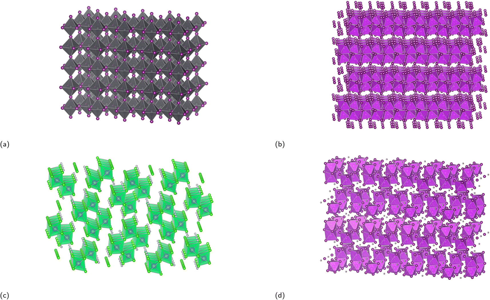 | ||
| Fig. 1 Crystal structure of (a) (MA)PbI3, (b) Rb3Bi2I9, (c) (MA)3Bi2Cl9, and (d) (MA)3Bi2I9 to present the dimensionalities of 3D, 2D, 1D, and 0D, respectively. The purple, green, and grey octahedra represent the octahedra of BiI6, BiCl6, and PbI6, respectively. The A-sites are omitted to elucidate the connectivity of the system. The structures in (b), (c), and (d) are taken from the ICSD database and have the collection code 90170, 109710, and 239297, respectively. | ||
In previous literature, concerns have been raised regarding the liberal use of the term ‘perovskite’ for compounds inspired by, but not structurally consistent with, the mineral perovskite structure.37,38 In this review, we introduce the term complex metal halide (CMH) to refer to such compounds. Here, CMH is a term based on composition rather than structure. Similar to the well-established term ‘complex metal oxides’, which describes metal oxides containing more than one metal,39–41 the term ‘complex metal halides’ denotes compositions that have at least three distinct components. These components include at least one elemental metal and one halide, with an optional organic component (for instance FA+, MA+, and long-chain alkyl monoammonium cations). CMHs include compounds such as (MA)3Bi2I9,42 Cs3Cu2I5,43, (MA)2KBiCl6,44 Cs2InAgCl6,45 and halide-based Ruddlesden–Popper phases (discussed in Subsection 3.1) that are of different dimensionalities.
The usage of the term CMH may include a wide range of materials, but it offers an alternative which would avoid current discrepancies regarding the use of the term perovskite. The term perovskite will, nevertheless, be used for compounds with a clear overall perovskite framework including distorted perovskites and ordered perovskites.38
Electronic dimensionality plays a crucial role in optoelectronic devices. Despite a CMH possessing a distinct structural dimensionality, its electronic dimensionality may still differ.46 This is seen for some double perovskites with the general formula A2B(I)B(III)X6, in which A and B(I) are monovalent cations, B(III) is a trivalent cation, and X is a halide anion. For B(I) = Na+, K+, Rb+ and B(III) = Bi3+, the inorganic octahedra are structurally connected in all three dimensions, but due to the B(I) cations not contributing to the band-edges, the octahedra are electronically isolated, resulting in a 0D electronic dimensionality.47
By reducing the bulk halide perovskite to crystals nanometers in size, one yields lower dimensional structures, which have shape-dependent form factor dimensionalities.
• 0D structures: these are structures that have zero dimensions in the sense that they are small, nanoscale particles or clusters, such as quantum dots or nanocubes (Fig. 2a).
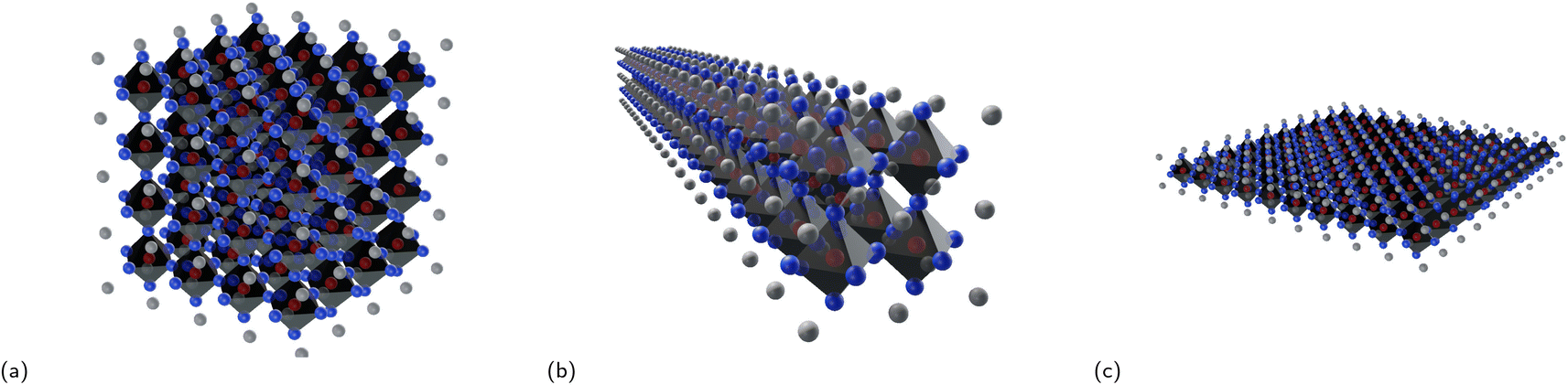 | ||
| Fig. 2 Crystal structure of three lower dimensional perovskites with varying form factors: (a) nanocube, (b) nanowire, and (c) nanosheet. The red, blue, and gray spheres represent the B-, X-, and A-site of a perovskite with the general formula ABX3, respectively. | ||
• 1D structures: these are structures that have one dimension that is much larger than the others, with the other two dimensions being on the nanoscale. Examples of 1D structures include nanowires, nanorods (Fig. 2b) and nanotubes.
• 2D structures: these are structures that have two dimensions that are much larger than the third, with the third dimension being on the nanoscale. Examples of 2D structures include nanoplatelets and nanosheets (Fig. 2c).
• 3D structures: these are structures that have three dimensions that are all comparable in size, and their size is typically much larger than the nanoscale. These structures can have any shape and are typically considered bulk materials.
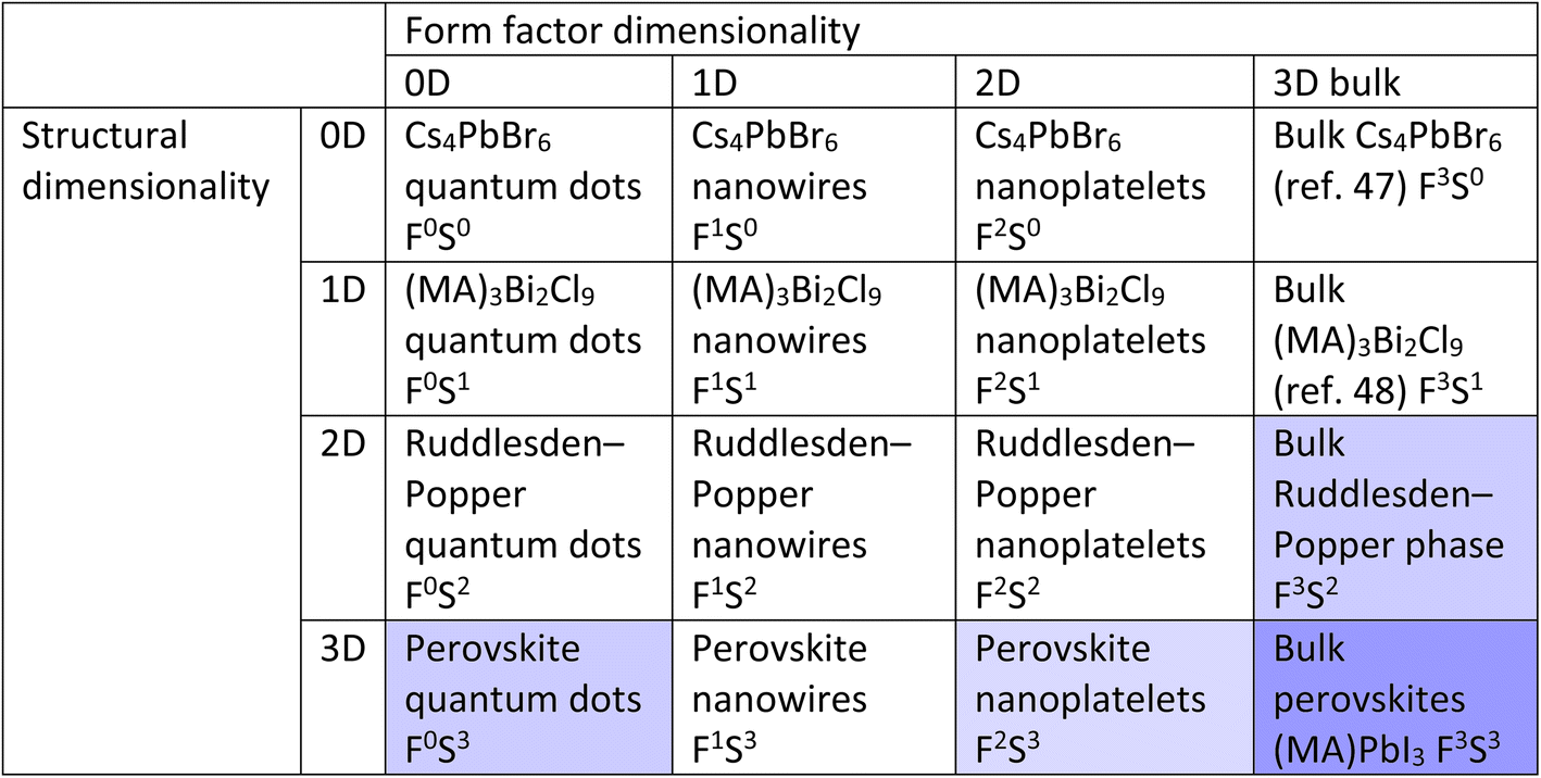
It becomes interesting when we conceptualize mixing structural dimensionality with form factor dimensionality. By doing so, we obtain a table such as that illustrated in Table 1. This table was inspired by the work of Cheetham and Rao, who created a similar classification system to explore the relationships between inorganic and organic connectivities.50Table 1 shows the 16 possible types of CMHs with mixed form factor and structural dimensionality. Note that the cells can be further extended if considering fractional dimensionalities such as 0.5, 1.5, and 2.5D. The notation FaSb is used where a and b represent the form factor and structural dimensionality of the compound, respectively. It is crucial to note that the table in no way reflects the trend in optoelectronic properties, since the electronic dimensionality is not taken into account here.
|
During the past few years bulk halide perovskites (F3S3 group) have certainly gained and enjoyed their spotlight within the field of photovoltaic research, but a lot of attention has shifted to lower dimensional compounds. To exemplify this using the proposed classification table, the avenues with the strongest research focus are highlighted in dark blue, whereas the avenues that are highlighted in light blue represent those with a mounting research interest. It is worth noting that the cells that are not highlighted do not correspond to avenues that have not been researched, but rather areas that have yet to be extensively studied, and have the potential for further research and exploration. In the subsequent paragraph, we will briefly compare bulk CMHs containing F3S3 dimensionality with their lower dimensional derivatives.
Bulk CsPbBr3 is renowned for its impressive absorption coefficient and superior charge carrier mobility, qualities that make them great candidate for light-harvesting applications. However, PLQYs of 3D halide perovskites is generally low. PLQY can be defined as  where rrad and rtot are the radiative recombination rate and the total recombination rate, including the non-radiative component, respectively. The reason for the low PLQY can be associated to a low exciton binding energy Eb, the energy required to separate an electrostatically coupled electron–hole pair.51 Bulk 3D perovskites have an exciton binding energy of around 10–50 meV, such that the excitons are dissociated at room temperature.52–54 The intrinsic properties of CMHs shift considerably when we modulate their form factor or structural dimensionality. This is evident when we decrease the dimensionality to that of bulk Cs4PbBr6 (F3S0) and colloidal CsPbBr3 with lower form factor dimensionality, for instance. Although both have reduced charge carrier mobility due to the confinement of charges, they compensate for this limitation by exhibiting significantly increased photoluminescence due to their higher exciton binding energies (more in Subsection 3.2). Taking the work from Bakr et al. as an example, in which CsPbBr3 and Cs4PbBr6 solids were synthesized and their PLQY determined, the former and latter materials displayed a PLQY of <0.1 and 45%, respectively.48 As for CMH with 3D structural and lower form factor dimensionalities such as lead-based perovskite nanocrystals (NCs), numerous studies have achieved high photoluminescence quantum yields (PLQYs) with PLQYs above 80% displayed for CsPbBr3 NCs.55–59 Decreasing the dimensionality of cesium bromoplumbates to F0S0 leads to a rather unexpected, yet intersting result. Uniform Cs4PbBr6 NCs around 26 nm in size were synthesized and demonstrated a PLQY of 65%,60 which is lower than the >80% observed for CsPbBr3 NCs. An astounding PLQY of 45% was obtained after drop-casting the Cs4PbBr6 NCs onto a glass slide. By contrast, the PLQY plummets from 56 to 18% when CsPbBr3 NCs were converted from colloidal to thin film form, likely due to aggregation or the loss of ligands.61 Nevertheless, low-dimensional compounds remain an underexplored area in material science, and investigation of lower dimensional classes of compounds might pave the way for uncovering materials that are both stable and at the same time possess outstanding properties.
This review focuses primarily on F3S2 corner-sharing haloplumbate octahedra-based CMHs, which have undergone extensive research, particularly in recent years. These structures exhibit tunable light-emission properties, enhanced stability in comparison to bulk 3D perovskites, and a potential to enhance device performance when integrated with a 3D perovskite layer, as demonstrated in photovoltaic devices.
3 2D structural dimensional CMHs
3.1 Ruddlesden–Popper phase
The Goldschmidt tolerance factor t (eqn (1)) is an empirical formula that can be used to predict whether a specific compound with the formula ABX3 adopts the cubic perovskite structure. Here, rA, rB, and rX are the ionic radius of the A-, B-, and X-site, respectively. The compound is expected to possess a cubic perovskite structure if t is between 0.8 and 1.0.62 However, since the tolerance factor is established based on the assumptions of the hard sphere model, it can only accurately predict compounds with lighter cations such as O2− and F−, and the model for compounds containing elements with low electronegativity and great chemical softness such as I− is less valid.63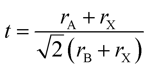 | (1) |
Currently, MA+ and FA+ are the only known organic cations that can be embedded into the halide perovskite structure while maintaining its three-dimensional perovskite framework. Using larger organic A-site cations results in the collapse of the 3D structure and the structural dimensionality is reduced.
One CMH containing a large organic group is the Ruddlesden–Popper (RP) phase. An RP phase has the general formula (RNH3)2(MA/FA)m−1BmX3m+1, where RNH3 is a large alkyl- or arylammonium group (widely known as the spacer cation). Its structure consists of a layered 2D inorganic framework with corner-sharing BX6 octahedra that is mainly held together between two spacer cation layers through hydrogen bonding between the hydrogen atoms of the ammonium group and the halide atoms.64 RP phases are of great interest primarily because they possess superior stability compared to 3D halide perovskites. In RP phases, the large hydrophobic organic groups that surround the water-soluble inorganic layers can be seen as encapsulation layers in the nanometer scale, enhancing the moisture stability of the structure.65m in the formula corresponds to the number of periodically-stacked inorganic sheets sandwiched between two adjacent organic layers. The number of inorganic layers between the organic groups can be tuned by modifying the stoichiometric ratio of the precursors. However, it is important to note that synthesis of RP phases (m ≠ 1) usually leads to not compounds of a single thickness m being formed, but rather a combination of m's, with 〈m〉 representing the average m value. To help the reader associate an RP phase with its respective spacer cation better, we present the chemical structure of organic spacer cations in Fig. 3.
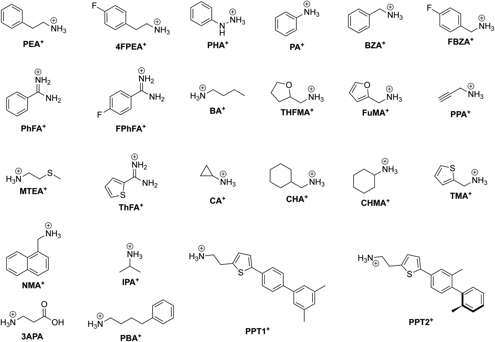 | ||
| Fig. 3 Chemical structure of relevant RP phase organic spacer cations along with their abbreviations labeled in bold. | ||
By varying the thickness of the inorganic layers, one can tune the electronic band gap of the system. Since the inorganic and organic layers act as potential wells and barriers, respectively, RP phases exhibit pronounced quantum confinement effects. Increasing the thickness of the well m increases the 3D nature of the system, causing a red-shift in the electronic band gap. For RP phases with low m values, these systems possess barriers with significantly lower dielectric constants than the wells. (C6H13NH3)2PbI4, for example, has dielectric constants of 2.1 and 6.1 for the organic and inorganic layers, respectively.66 The difference in dielectric constants leads to dielectric confinement effect, which is also referred to as image charge effect.67 The combination of quantum and dielectric confinement increases the optical band gap of the material.68 Just as well thickness affects absorption, it also governs emission properties. Increasing m induces a redshift in emission, establishing a direct correlation with well thickness and emitted wavelength (Fig. 4). To elucidate the correlation between well thickness and optical properties of RP phases, we included Fig. 5 that shows both the emission (depicted by a solid line) and absorption (represented by a dashed line) spectra of the (BA)2MAm−1PbmI3m+1 family, where BA+ is butylammonium and m ranges from 1 to 5.69 The band gap of the m = 2, 3, 4, and 5 phases are 2.17, 2.03, 1.91, and 1.83 eV, respectively.
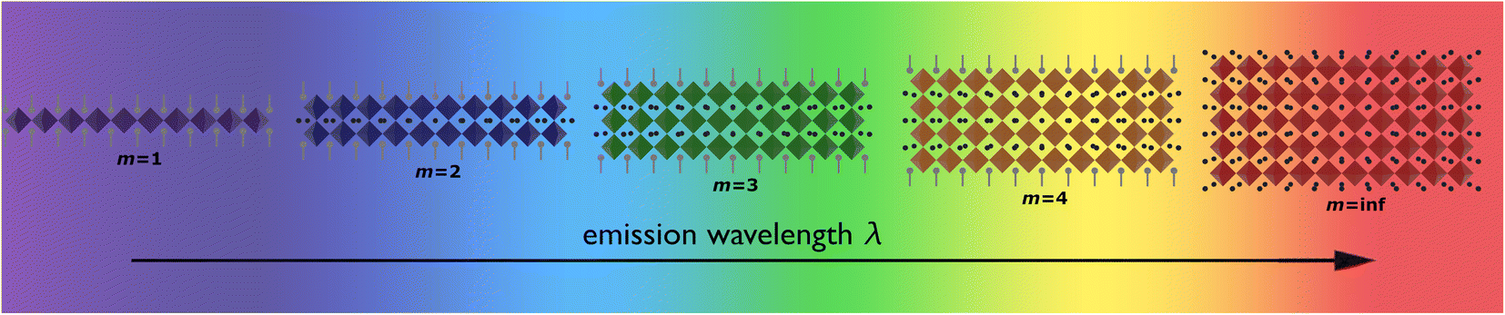 | ||
| Fig. 4 Illustration displaying the relationship between the layer of quantum wells (m) and emission wavelength. | ||
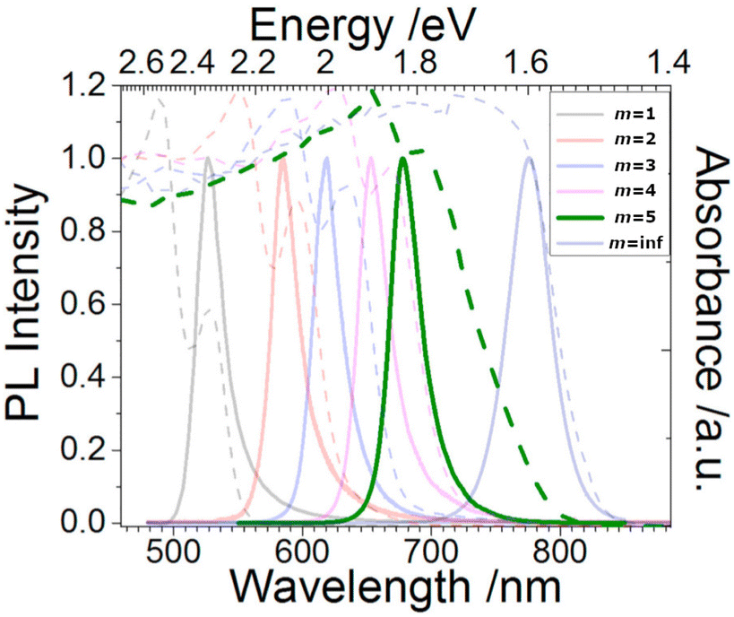 | ||
| Fig. 5 Optical absorption (dashed line) and emission (solid line) spectra of the (BA)2MAm−1PbmI3m+1 (m = 1–5) family and (MA)PbI3 (m = inf.). Reproduced with permission.69 Copyright 2017, Cell Press. | ||
Since RP phases for which m = 1 can be conceptualized as the product of cutting a 3D halide perovskite along the (100) plane to yield a single-layer of [BX4] framework, these compounds are often referred to as pure 2D perovskites.70,71 RP phases for which m > 1 are commonly known as quasi-2D perovskites, as these compounds contain a combination of methyl ammonium and large organic ammonium cations that, when reacted with salts such as PbX2, lead to the formation of compounds with 3D and 2D structural dimensionality, respectively. The dimensionality of the system approaches 3D, which is that of bulk perovskite, when m approaches ∞. Although the terms 2D and quasi-2D perovskites are often used in related literature, this review will not employ these terms.
3.2 Exciton binding energy
The exciton binding energy of a complex halide EB with a dimensionality α can be calculated using the following formula: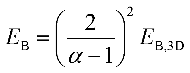 | (2) |
Decreasing the well width, i.e., the thickness of the inorganic layer, increases the band gap along with the exciton binding energy as a result of the spatial confinement and image charge effect, in which the effective Coulomb charge between the electron and hole in the inorganic layer is increased.77,78 For instance, the energy diagram of (BA)2(MA)m−1PbmI3m+1 (m = 1–5) using ultraviolet photoelectron spectroscopy (UPS) and inverse photoelectron spectroscopy (IPES) to determine the valence band maximum (VBM) and conduction band minimum (CBM) of the RP phase series, respectively, was presented by Zhong et al.79 Their experimental results are in good agreement with the computed work using density functional theory (DFT) and shows a clear decrease in band gap with increasing m value. Although low m-values are often associated with better stability due to more hydrophobic spacer cations being present, they are also indicative of low charge mobility and short carrier lifetime.80 The compromise between the photovoltaic device performance and the stability of the composition, denoted by a low value of the inorganic layer (for Dion–Jacobson phases n is used as opposed to m), is presented in Table 3. Dion–Jacobson (DJ) phase structures will be elaborated on in Subsection 3.7. To avoid the abovementioned issues that comes with a low m-value and at the same time obtaining an absorption spectrum that significantly coincides with the solar irradiance spectrum, m-values between 3 an 5 are often used.81
One of the synthesis challenges of 2D CMHs such as RP phases is achieving phase-pure films, i.e., films containing only the desired m value and not a combination of them. Phase-pure films generally exhibit much clearer and sharper (0k0) planes than their more randomly-oriented counterpart. Another synthesis challenge is the self-assembly of the conductive 2D inorganic framework such that the inorganic sheets align perpendicular to the surface of the electrode or substrate, allowing for efficient charge transport. The reason for this is because orientation of inorganic layers deviating from vertical orientation prohibit charge carrier to migrate to the electrodes, since these cannot migrate through electrically insulating organic spacer cations.82 Vertical and horizontal orientation refer to the perpendicular and parallel alignment of the inorganic layers to the electrode surface, respectively. There also exists partial random orientation, also known as mixed orientation, in which the inorganic sheets are aligned in random directions. Chen and coworkers synthesized the compound (BA)2(MA)3Pb4I13 with different degrees of preferential orientation of the 2D inorganic layers using spin-coating-annealing process by simply modifying the duration of the spin-coating process.75 20 and 60 s of spin-coating resulted in the formation of strongly vertically orientated and randomly oriented 2D inorganic slabs, respectively, which was determined using wide angle X-ray scattering (GIWAXS). The solar cell constructed using a vertically oriented thin film displayed higher short circuit current density (JSC), lower series resistance RS, and a much improved device performance compared to its randomly oriented counterpart. An illustration of two orientation types, as seen in Fig. 6a and b, is presented to help demonstrate the effect of film orientation on charge carriers. In the early stages of RP phase research for light-harvesting applications, Tsai et al.'s paper made a notable contribution by identifying the increase in vertical orientation of the RP phase using hot-casting technique, which essentially means spin coating the precursors at higher substrate temperatures, increasing the vertical orientation of (BA)2(MA)2Pb3I10 and (BA)2(MA)3Pb4I13 films.82 The optimal substrate temperature, at which the crystallinity of the films is superior, was shown to be at 110 °C.
 | ||
| Fig. 6 Illustration of a film consisting of an RP phase between the electron transport layer (ETL) and the hole transport layer (HTL) with a (a) (left) strong vertical orientation and a (b) (left) partial random (mixed) orientation as supported by GIWAXS data ((a) (right) and (b) (right)). Reproduced with permission.75 Copyright 2018, Springer Nature. Illustration of two RP phases, each with a different phase distribution type: (c) ordered distribution and (d) random distribution. Reproduced with permission.76 Copyright 2020, John Wiley and Sons. | ||
3.3 RP phase for photovoltaic applications
A quite commonly used spacer cation is 4-fluoro-phenethylammonium (4FPEA+). Utilizing fluorinated spacers was demonstrated to be able to greatly enhance device properties. This was well exemplified by Wang and coworkers, where the fluorinated spacer 4FPEA+ cation was compared to their non-fluorinated, chlorinated, and brominated derivatives.76 The device with (4FPEA)2(MA)3Pb4I13 exhibited a PCE of 18.10%, whereas the devices with non-fluorinated, chlorinated, and brominated counterparts had a PCE of 12.23, 7.93, and 6.08%, respectively. The substitution to the fluorinated spacer led to better film crystallinity, more vertically-oriented film, increased visible absorption, lower exciton binding energy, and also prevented formation of the m = 1 phase. Notably, halogen substitution resulted in the formation of RP phases with different phase distribution types, as shown in Fig. 6c and d. While PEA+- and 4FPEA+-based films have a more ordered phase distribution (Fig. 6c), the films based on their chlorinated and brominated counterparts have a more random phase distribution (Fig. 6d). Ordered phase distribution results in graded band alignment, facilitating efficient electron transfer from phases with small m-values to phases with large m-values. In contrast, films with a random phase distribution have a mismatched band alignment, inhibiting electron transport and causing carrier accumulation.Increased intermolecular interactions between the spacer cations were shown to enhance carrier transport properties and stabilization. A solar cell with a dense, pinhole-free film of (MTEA)2(MA)4Pb5I16 (MTEA+ = 2-(methylthio)ethylammonium) acting as the photosensitizer, was built and exhibited PCEs as high as 18.06%.83 The film exhibited good light resistance as well as thermal and moisture stability. The reason for improved stability is likely associated with the presence of sulfur–sulfur interaction, which is also believed to induce vertically oriented growth of the inorganic layer.
Near-single-phase RP phase compounds with the formula (BA)2(MA)m−1PbmI3m+1 (〈m〉 = 1, 2, 3, 4, 5) were synthesized by employing the molten salt spacer n-butylamine acetate (BAAc) instead of traditional halide spacers such as BAI.84 Several characterization methods were used to confirm the successful synthesis of the almost phase-pure films, including transient absorption (TA) and GIWAXS measurements. Compared to films with the same composition synthesized using the traditional precursor BAI, the near-single-phase RP phase films exhibited a larger average grain size and displayed no pinholes. The presence of the molten salt spacer led to a uniformly distributed intermediate phase in the form of a gel being formed in the initial stage of the synthesis, which explains the formation of the near-single-phase films. Furthermore, the grains were also shown to be vertically aligned. A maximum PCE of 16.25% was achieved for the solar cell with a BAAc-synthesized RP phase film (〈m〉 = 4).
Shao et al. constructed a highly stable solar cell with a PCE of 21%, which is the highest recorded PCE of an RP phase-based solar cell to date.86 Instead of the traditionally incorporated MA+ cations for the RP phase structures, FA+ was used and showed improved device stability while retaining high efficiencies. More information on its device stability can be extracted from Table 2, which displays recently reported RP phase-based solar cells containing high PCEs. The table includes information on the device performance and stability of RP phase-based solar cells, and allows for easy comparison between different monoammonium cation groups.
| Spacer cation | Composition | Device structure | PCE (%) | Stability | Ref. |
|---|---|---|---|---|---|
| a FTO: fluorine-doped tin oxide, PEDOT:PSS: poly(3,4-ethylenedioxythiophene)-poly(styrenesulfonate), PC61BM: [6,6]-phenyl-C61-butyric acid methyl ester, BCP: bathocuproine, ITO: indium-doped tin oxide, PTAA: poly[bis(4-phenyl)(2,4,6-trimethylphenyl)amine], PEI: polyethylenimine, spiro-OMeTAD: 2,2′,7,7′-tetrakis(N,N-di-p-methoxyphenyl-amine)-9,9′-spirobifluorene. | |||||
| Phenethylammonium (PEA+) | (PEA)2(MA)3Pb4I13 | FTO/PEDOT:PSS/RP phase/PC61BM/BCP/Ag | 18.5 | Unencapsulated device: ca. 90% of initial PCE after 1200 h of exposure to relative humidity of 40% | 153 |
| 4-Fluoro-phenethylammonium (4FPEA+) | (4FPEA)2(FA)4Pb5I16 | ITO/PTAA/RP phase/PC61BM/BCP/Ag | 21.07 | Unencapsulated device: 97% of initial PCE after 1500 h of heating at 85 °C in N2 atmosphere. Encapsulated device: ca. 92% of initial PCE after 3000 h of exposure to relative humidity of 40 ± 5% | 86 |
| (4FPEA)2(FA0.3MA0.7)4Pb5I16 | ITO/PTAA/RP phase/PC61BM/BCP/Ag | 20.07 | Unencapsulated device: 92% of initial PCE after 1500 h of heating at 85 °C in N2 atmosphere. Encapsulated device: ca. 81% of initial PCE after 3000 h of exposure to relative humidity of 40 ± 5% | 86 | |
| (4FPEA)2(MA)4Pb5I16 | ITO/PTAA/RP phase/PC61BM/BCP/Ag | 17.05 | Unencapsulated device: 78% of initial PCE after 1500 h of heating at 85 °C in N2 atmosphere. Encapsulated device: ca. 66% of initial PCE after 3000 h of exposure to relative humidity of 40 ± 5% | 86 | |
| (4FPEA)2(MA)4Pb5I16 | ITO/PTAA/RP phase/PC61BM/PEI/Ag | 18.67 | Unencapsulated device: 87% of initial PCE after 35 days of exposure to 40% relative humidity at room temperature | 154 | |
| (4FPEA)2(MA)3Pb4I13 | ITO/PTAA/RP phase/PC61BM/PEI/Ag | 18.10 | Unencapsulated device: more than 90% of initial PCE after exposure to 40–50% relative humidity for 30 days and 80% of initial PCE after heating at 80 °C in N2 atmosphere for 30 days | 76 | |
| 2-Phenylhydrazin-1-ium (PHA+) | (PHA)2Cs4Pb5I16 | FTO/TiO2/RP phase/spiro-OMeTAD/MoO3/Ag | 16.23 | ca. 70% of initial PCE after 30 h of heating at 80 °C. ca. 50% of initial PCE after 40 h of exposure to relative humidity of 30–35% | 155 |
| Phenylammonium (PA+) | (PA)2Cs4Pb5I16 | FTO/TiO2/RP phase/spiro-OMeTAD/MoO3/Ag | 14.56 | ca. 20% of initial PCE after 30 h of heating at 80 °C. Essentially 0% PCE after 40 h of exposure to relative humidity of 30–35% | 155 |
| Benzylammonium (BZA+) | (BZA)2(MA)m−1Pbm(ClxI1−x)3m+1 mixed m, m = 1–4 | ITO/PTAA/RP phase/PC61BM/PEI/Ag | 12.39 | Unencapsulated device: ca. 60% of initial PCE after 35 days of exposure to 40% relative humidity at 25 °C | 156 |
| 4-Fluoro-benzylammonium (FBZA+) | (FBZA)2(MA)m−1Pbm(ClxI1−x)3m+1 mixed m, m = 1–4 | ITO/PTAA/RP phase/PC61BM/PEI/Ag | 16.82 | Unencapsulated device: over 80% of initial PCE after 35 days of exposure to 40% relative humidity at 25 °C | 156 |
| Benzamidinium (PhFA+) | (PhFA)2(MA)4Pb5I16 | ITO/PEDOT:PSS/RP phase/PCBM/BCP/Ag | 12.92 | Unencapsulated device: 68% of initial PCE after 3000 h of storage in N2 atmosphere and 77% of initial PCE after 450 h of continuous illumination at 100 mW cm−2 in N2 environment | 157 |
| 4-Fluoro-benzamidinium (FPhFA) | (FPhFA)2(MA)4Pb5I16 | ITO/PEDOT:PSS/RP phase/PCBM/BCP/Ag | 17.37 | Unencapsulated device: 99% of initial PCE after 3000 h of storage in N2 atmosphere and 82% of initial PCE after 450 h of continuous illumination at 100 mW cm−2 in N2 environment | 157 |
| Butylammonium (BA+) | (BA)2(MA)4Pb5I16 | ITO/PTAA/RP phase/C60/BCP/Ag | 17.66 | Unencapsulated device: 86.7% of initial PCE in nitrogen atmosphere after 1000 h | 158 |
| (BA)2(FA)3Pb4I13 | FTO/SnO2/RP phase/spiro-OMeTAD/Au | 18.14 | Unencapsulated device: 93.3% of initial PCE after 720 h of exposure to 40% relative humidity at 85% | 159 | |
| (BA)2(MA)4Pb5I16 | ITO/PTAA/RP phase/C60/BCP/Ag | 18.04 | Unencapsulated device: 85% of initial PCE after more than 500 h of heating at 60 °C in N2 | 160 | |
| (BA)2(MA)3Pb4I13 | ITO/PEDOT:PSS/RP phase/PC61BM/BCP/Ag | 16.48 | Unencapsulated device: ca. 80% of initial PCE after 3200 min of exposure to 55–60% relative humidity while being under continuous 1 sun illumination. After 34 days, the device stability retains ca. 89% and 91.6% of initial PCE after exposure to 55–60% relative humidity and after exposure to continuous heating at 85 °C, respectively | 161 | |
| (BA)2(MA)3Pb4I13 | ITO/SnO2/RP phase/spiro-OMeTAD/MoO3/Au | 16.25 | Unencapsulated device: 93.8% of initial PCE after 4680 h of exposure to 65 ± 10% relative humidity, 95.7% of initial PCE after continuous heating at 85 °C for 558 h in N2 atmosphere, and 96.2% of initial PCE after continuous illumination at AM1.5 G for 1100 h | 84 | |
| (Tetrahydrofuran-2-yl)methanammonium (THFMA+) | (THFMA)2(MA)3Pb4I13 | ITO/PEDOT:PSS/RP phase/PC61BM/BCP/Ag | 13.79 | Unencapsulated device: 80% of initial PCE after 934 h of storage in N2 and 63% of initial PCE after 528 h under continuous light illumination in N2 | 162 |
| Furan-2-ylmethanammonium (FuMA+) | (FuMA)2(MA)3Pb4I13 | ITO/PEDOT:PSS/RP phase/PC61BM/BCP/Ag | 18.00 | Unencapsulated device: 94% of initial PCE after 1850 h of storage in N2, 83% of initial PCE after 768 h at 85 °C in N2, and ca. 80% of initial PCE after 768 h under continuous light illumination in N2 | 162 |
| (FuMA)2Cs4Pb5I16 | ITO/SnO2/RP phase/spiro-OMeTAD/Au | 15.66 | Unencapsulated device: 94.0% of initial PCE after 1640 min at 85 °C in ambient atmosphere and 83.5% of initial PCE after 1800 h of exposure to 5–10% relative humidity at room temperature | 163 | |
| Prop-2-yn-1-ammonium (PPA+) | (PPA)2(MA)2Pb3I10 | ITO/PTAA/RP phase/C60/Al | 15.20 | Unencapsulated device: 60% of initial PCE after 600 h in N2 atmosphere | 164 |
| 2-(Methylthio)ethylammonium (MTEA+) | (MTEA)2(MA)4Pb5I16 | ITO/PEDOT:PSS/RP phase/PC61BM/Cr/Au | 18.06 | 87.1% of initial PCE for 1000 h at 0.9 V | 83 |
| Amino(thiophen-2-yl)methaniminium (ThFA+) | (ThFA)2(MA)2Pb3I10 | ITO/PEDOT:PSS/RP phase/PC61BM/BCP/Ag | 16.72 | Unencapsulated device: over 99% of initial PCE after 3000 h in N2 and 90% of initial PCE after 216 h of continuous light soaking | 165 |
3.4 RP phase 2D/3D perovskite junction
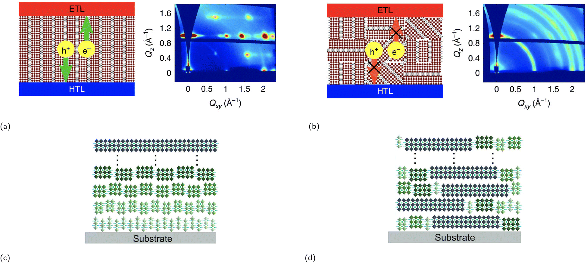
Record PCEs of solar cells based on RP phases are lower than 3D halide perovskites due to several factors such as larger band gaps, increased exciton binding energies, and poor charge transport.87,88 Achieving an even greater PCE, comparable to that of a 3D halide perovskite, while simultaneously maintaining a good stability can be accomplished by incorporating RP phases to 3D halide perovskites, i.e., mixing 2D with 3D CMHs. By doing so, one combines the superior optoelectronic properties of 3D halide perovskites with the exceptional structural stability of RP phases. There are generally two methods to integrate the two different dimensionality types: either doping the 2D compound into the 3D system or creating a distinct 2D layer on top of the 3D perovskite structure, as illustrated in Fig. 7a. This review will exclusively focus on the latter method. The formation process of the RP phase 2D/3D perovskite junction typically involves solution processing, e.g., spin-coating a thin layer of an organic cation salt (e.g., (PEA)I, (BA)I, (MTEA)I) onto the 3D layer. This action facilitates the creation of a 2D passivation layer upon thermal annealing through its interaction with the excess lead halide situated on the 3D film's surface. It is, however, imperative that the solvent chosen to dissolve the organic component does not dissolve or destroy the underlying film. Consequently, isopropyl alcohol is commonly selected for this purpose. A PV device containing such hybrid structure was first reported by Shi et al. in 2016.89 The group covered a (MA)PbIxCl3−x thin film with a layer of (CA)2PbI4 (CA+ = cyclopropylammonium) by spin coating a solution of CAI in IPA, and the resulting PV device displayed a PCE of 13.86%, similar to that of the 3D perovskite, but with an improved stability. In terms of its stability, the hybrid device retained 54% of its stability in a 63 ± 5% humidity condition for 220 h, whereas the PCE of the fully 3D perovskite-based device dropped to 0% within only 50 h.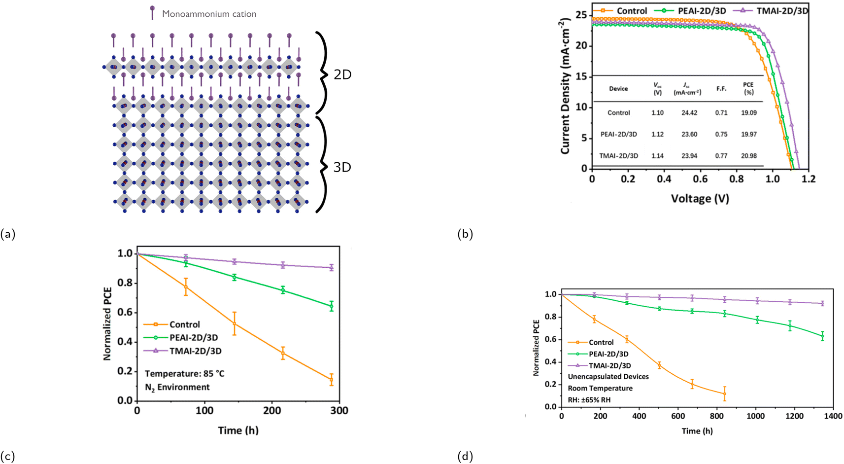 | ||
| Fig. 7 (a) Crystal structure illustration of a 2D/3D heterojunction. (b) Graph (including table) displaying the difference in photovoltaic performance of three different devices. Control refers to the device containing solely an alloyed perovskite as the active layer, whereas PEAI-2D/3D and TMAI-2D/3D correspond to the device with a perovskite/PEA2PbI4 and a perovskite/TMA2PbI4 layer, respectively. Graphs demonstrating the stability of the three devices over time under the following conditions: (c) N2 environment at 85 °C and (d) relative humidity (RH) of 65%. Reproduced with permission.85 Copyright 2021, American Chemical Society. | ||
The inclusion of the 2D RP phase on top of the 3D perovskite film can lead to improvements in charge extraction and increase PCE. This was, for example, reported in a recent paper where the addition of an RP phase with cyclohexylammonium (CHA+) and cyclohexylmethylammonium (CHMA+) as the spacer cation between (FA)PbI3 and spiro-OMeTAD led to an increase in VOC, FF, JSC, and the PCE.90 The PCE increase from 20.41 to 23.91% of the solar cell with an RP phase layer based on CHMA+ on top of the (FA)PbI3 layer was observed as a result of the reduction in both surface recombination and interfacial resistance.
He and coworkers investigated incorporating an RP phase with a sulfur-containing spacer cation, 2-thienylmethylammonium (TMA+), onto a 3D perovskite by constructing three different devices: one without the 2D RP phase passivation layer and only the 3D alloyed perovskite Cs0.05(FA0.83MA0.17)0.95Pb(I0.83Br0.17)3 (labeled as control), one with a PEA2PbI4 passivation layer, and one with a TMA2PbI4 passivation layer.85 Addition of the sulfur-containing 2D layer resulted in a lower trap state density, longer carrier lifetime, enhanced thermal, and moisture stability. The effect of incorporating the RP phase into a 3D perovskite is emphasized by Fig. 7b–d, which display enhancement in both device performance and stability.
In a recent study, Mohite et al. proposed a criterion for selecting solvents suitable for organic cation salts, basing their choice on the dielectric constant, denoted as ε, and the Gutmann number, DN.91 While ε primarily quantifies the solvent's ability to dissolve ionic compounds, the Gutmann number DN signifies the solvent's Lewis basicity. For effective 2D layer deposition, without altering the underlying 3D perovskite layer, the group proposes a value of ε exceeding 30 and the Gutmann number DN ranging from 5 to 18 kcal mol−1 for the solvent. While several solvents meet these criteria, including acetonitrile, tetramethyl sulfone, and propylene carbonate, acetonitrile was selected for the organic cation to be dispersed in due to its high volatility, which is attractive for low-temperature processing. Pure (BA)2(MA)m−1PbmI3m+1 crystals with m = 1 to 4 were grown, its powders dissolved in acetonitrile, and the film deposited onto Cs0.05(FA)0.85(MA)0.10Pb(I0.90Br0.10)3. A photovoltaic device with a 2D/3D junction based on (BA)2MA2Pb3I10 was constructed and exhibited a remarkable champion PCE of 24.5%. Furthermore, the device maintained 99% of its initial PCE even after an impressive duration of over 2000 hours.
Also here, the challenge of orientation control of the RP phase crystallites, persists. Different to a photovoltaic device based on solely the 2D RP phase as the active layer, studies show that solar cells with hybrid systems, in which the 2D layers are horizontally aligned to the 3D perovskite film surface, can improve device efficiency.94–96 The influence of spacer cations on the crystallite orientation of RP phases deposited on a triple-cation perovskite was investigated.94 Salts of the organic spacers 4FPEA and PEA deposited on a triple-cation perovskite led to mixed and horizontal orientation of the resulting RP phase, respectively. The orientation of the quantum wells is of great importance, since from TA analysis it was established that electron dissociation takes place from the 2D RP phase to the 3D perovskite. The solar cell incorporating horizontally oriented RP phases exhibited an improved VOC compared to the device with randomly oriented crystallites, attributed to a reduction in charge recombination. As such, horizontal orientation can improve device performance and passivate the 3D film more efficiently than mixed orientation.
In 2022, Choi and colleagues reported a PV device based on a (BA)2(MA)m−1PbmI3m−1Br2 active layer that was fabricated by depositing BABr using vapor- and solution-based deposition methods onto a vacuum-deposited (MA)PbI3 layer.97 The difference between depositing (BA)Br using a vapor- and solution-based method showed significant difference. The former method led to the formation of a highly vertically oriented RP phase layer, whereas using the latter method hindered the growth of finely oriented RP phases. Herein, the PCE of the solar module with a vacuum-deposited passivation layer displayed a PCE of 21.4%. The highest reported PCE among all PSCs with a vacuum-processed passivation layer was reported recently using vacuum flash method incorporating 3-ammonium propionic acid (3APA+) as the spacer cation.98 The resulting device with a hybrid dimensionality achieved a PCE as high as 24.72% and retained 96.1% of its PCE after 1400 h of continuous operation under one sun illumination.
A solar cell with an intact 2D/3D CMH junction, displaying an impressive PCE of 24.35%, using a so-called solid-state in-plane growth (SIG) was fabricated and reported in 2021.99 Unlike conventional solution-processing methods, SIG is based on a solid-state method, in which a solid-state 2D film is stacked onto a 3D film. This is followed by crystal growth of the 2D phase above the 3D layer under pressure and heat and the detachment of the original 2D precursor after the complete growth of the 2D crystals in the in-plane direction. This proposed method of forming such intact 2D/3D junctions has the advantage of the ability to adjust the thickness of the 2D layer, preventing the formation of any unwanted phase that has a negative effect on the device performance and stability.
Some other notable works on engineering solar cells based on 2D/3D CMH junctions include the incorporation of 4FPEA+,100 phenylpropylammonium,101 and 2-thiophenemethylammonium102 as spacer cations.
3.5 RP phases for LED applications
Since both lead-based CMHs with reduced form factor dimensionality and RP phases have a more efficient electroluminescence (EL) than 3D perovskites due to their larger EB and thus faster radiative recombination, these materials have been extensively researched for LED applications.103 Whilst LED devices based on the former material as the active layer have at the time of writing this review achieved an EQE of almost 30%,104,105 LEDs incorporating films of the latter compound as the active layer have achieved impressive EQEs exceeding 20%.106–108 The EL of RP phases can be tuned by varying the halide ratios or the average thickness of the inorganic layers 〈m〉 (Fig. 8).92 These characteristics alongside the ease and low cost of RP phase synthesis render them highly promising as materials for LED devices. It is, however, important to note that halide mixing in low-dimensional compounds CMHs such as RP phases causes emission instability due to halide ion migration.109 Since 2016, extensive research efforts have been dedicated to investigating RP phases with varied color emissions for LED applications. These include studies on red emissions,110–112 green emissions,93,113 and blue emissions.114–116 Blue RP phase emitters, however, lag behind their red and green counterpart mainly due to increased electron–phonon coupling and trap-mediated non-radiative recombination, less efficient energy transfer, and interface fluorescence quenching.117,118 We will begin our discussion by examining a select few significant works from the initial stages of RP phase research as LEDs. Following this, a more recent contribution will be covered as well. | ||
| Fig. 8 (a) EL tuning of FA+-based RP phases between 666 and 740 nm by varying the Br:I ratio and/or 〈m〉. Reproduced with permission.92 Copyright 2018, Nature Publishing Group. (b) Phase distribution of an engineered energy landscape with 〈m〉 = 3. Reproduced with permission.93 Copyright 2017, American Chemical Society. | ||
The PLQY of the (PEA)2(MA)m−1PbmI3m+1 family was investigated at a low excitation intensity of 6 mW cm−2 by Sargent and coworkers in 2016.119 Notably, whilst very low PLQY values of around 0.1–0.2% were observed in m = 1 and m = ∞, 〈m〉 = 3 and 〈m〉 = 5 exhibited a much higher PLQY of 10.1 and 10.6%, respectively. A carrier funneling process was suggested to be the main reason why higher PLQYs are observed for 〈m〉 = 3 and 〈m〉 = 5. Since different m values were identified in 〈m〉 = 3 and 〈m〉 = 5, the presence of these multiphases (also referred to as multiple quantum wells or MQWs) enables a downward energy funneling process, in which carriers are transferred to and concentrated at low band gap emitters. The energy cascade from high to low band gap emitters occur on the picosecond timescale and is faster than non-radiative recombination.120 The carrier funneling process out-competes trap-mediated non-radiative recombination and at the same time enhances radiative recombination rate. A device based on the 〈m〉 = 5 compound was built, for which the external quantum efficiency (EQE) and the radiance reached 8.8% and 80 W sr−1 m−2, respectively. Huang and coworkers reported an LED device based on an active layer composed of self-assembled MQWs with high EQEs in the same year.120 The LED device with (NMA)2(FA)Pb2I7 (〈m〉 = 2, NMA+ = naphthalen-1-ylmethanammonium) as the active layer exhibited an EQE of up to 11.7%, an energy conversion energy efficiency of 5.5%, and a current density of 100 mA cm−2. Fig. 8b depicts the phase distribution of an MQW with an engineered energy landscape, in which the number of phases decreases with increasing well thickness.93 This figure provides insight into the optimized conditions for efficient energy transfer within the system. Fig. 9a illustrates the charge transfer process within a system predominantly composed of one distinct phase, which is also referred to as a flat energy landscape. By contrast, a simplified visual depiction of the transfer process of an engineered energy landscape is presented in Fig. 9b. Herein, the fast charge transfer from wide to low band gap phases suppresses trap-mediated non-radiative recombination. This energy cascade is observed when simulating the time evolution of photoexcited states of a MQW using Monte Carlo simulation (Fig. 9d). In comparison, the same simulation of a system with a flat energy landscape gives a rather different result, wherein mainly non-radiative recombination is observed due to charge trapping (Fig. 9c).
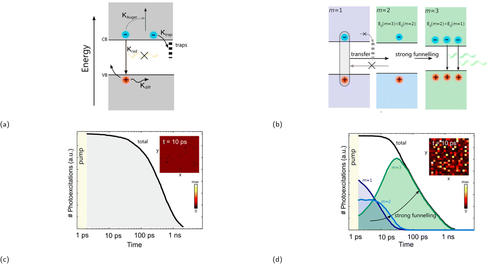 | ||
| Fig. 9 (a) Diagram showing charge either trapped, lost via Auger recombination, or undergoing radiative recombination in a flat energy landscape. κ represents the rate of the aforementioned processes. (b) Diagram displaying charge funneling process being the primary process in an engineered energy landscape, since these occur faster than trap-mediated non-radiative recombination. Recombination kinetics of (c) a flat energy landscape and (d) an engineered energy landscape using stochastic Monte Carlo simulation. The insets in (c) and (d) show the distribution of excited states within a 200 × 200 nm area 10 ps after excitation. Reproduced with permission.93 Copyright 2017, American Chemical Society. | ||
In 2018, an impressive PLQY of 88% was attained for a (PEA)2(Cs0.75(MA)0.25)1.25Pb2.5Br8.5 film, incorporating 40% (IPA)Br additive (IPA+ = iso-propylammonium).121 This film, characterized by a sky-blue emission and a PL peak at 477 nm, comprises a blend of various phases (m = 1, 2, 3, 4, 5, and higher). LED devices were fabricated using the mixed A-site system, featuring diverse film thicknesses for the active layer. Notably, the device employing the thinnest film (40 nm) exhibited increased current density and luminance. Thinner films are advantageous as they ensure an adequate number of charge carriers reach the recombination zone, a crucial factor for RP phases with generally lower conductivity compared to 3D perovskites. Despite these advancements, the maximum recorded EQE, energy power efficiency, and power efficiency for the devices were 1.5%, 0.92 lm W−1, and 2.8 cd A−1.
High quality single crystals of (R)2PbBr4 with deep blue emission consisting of different aliphatic and phenyl groups in the organic cation was explored, with a focus on (PEA)2PbBr4 and (BA)2PbBr4.122 Higher crystal rigidity of the RP phase with the aromatic component was confirmed, with slower non-radiative recombination rate and higher PLQY observed in (PEA)2PbBr4 relative to (BA)2PbBr4. A PLQY as high as 79% was shown in (PEA)2PbBr4. It is worth noting that the crystals studied here contain low defect densities, such that much higher efficiencies can be obtained compared to polycrystalline materials, for example. The higher crystal rigidity of the system, dependent on the organic cation identity, can result in higher PLQY, since it is associated to weak electron–phonon coupling.
While the highest recorded EQEs for blue LEDs incorporating RP phases remain around 15%,123,124 green and red LEDs with RP phases have not only reached but, in some cases, even surpassed an impressive EQE of 26%.92,123,125,126 A deep-red LED with a record efficiency of 26.3% was constructed by introducing large π-conjugated systems capable of suppressing ion migration, improving phase control, reducing defect densities, as well as increasing radiative recombination efficiencies.92 The cations PPT1+ (2-(5-(3′,5′-dimethyl-[1,1′-biphenyl]-4-yl)thiophen-2-yl)ethyl-1-ammonium) and PPT2+ (2-(5-(2,2′-dimethyl-[1,1′-biphenyl]-4-yl)thiophen-2-yl)ethyl-1-ammonium) were introduced as the A-site in A2PbI4 and displayed significantly improved coverage and stability against ion diffusion than the same A2PbI4 system with A+ = BA+ and TEA+. Subsequently the formamidinium-based systems A2(FA)2Pb3I10 (〈m〉 = 3) were synthesized and characterized, with only the PPT1-based system exhibiting a narrow phase distribution, resulting in both a blue shift in emission and improved PLQY. A faster energy transfer from high to low band gap emitters of around 0.2 ps was observed, which is associated with improved phase purity and lower defect density.
To achieve high-efficient blue-emitting LEDs based on RP phases, modulating the phase distribution by suppressing the formation of small m phases such as m = 1, 2 to reduce electron–phonon coupling and increasing that of other small m phases such as m = 3, 4 is essential.117 To give an example, Zhang et al. employed a pre-deposted guanidine thiocyanate film to control the phase distribution of (PBA)2Csm−1PbmBr3m+1 (PBA+ = 4-phenylbutylammonium) films.124 This method led to an inhibition of m = 1, 2 phases, prevented the overgrowth of large m phases, and also passivated film defects. An optimized LED device containing the MQW film with modulated phase distribution displayed an EQE of 16.40% and a maximum luminance of 8290 cd m−2.
3.6 RP phases for other optoelectronic applications
As covered above, RP phases containing MQWs with narrow phase distribution possess a fast energy cascade, such that charge carriers are concentrated at phases with higher m-values. The reduction in trap-mediated non-radiative recombination rate and a build-up of population inversion due to charge carrier localization in low band gap phases make RP phases a great candidate for lasing applications. The intrinsic gain properties of RP phase in the form of thin films were first reported in 2018.127 (NMA)2(FA)Pb2I7 (〈m〉 = 2) was shown to possess tunable amplified spontaneous emission (ASE) in the 530–810 nm range, achieving ASE at a low threshold of 8.5 ± 0.5 μJ cm−2 as well as a gain coefficient of as high as >300 cm−1. Since then, many investigations have been undertaken to enhance the understanding of RP phases for lasing applications.128–132 Within the visible wavelength range, lead-based 3D perovskite systems showcase ASE thresholds that are roughly an order of magnitude higher compared to those observed in systems with MQWs.133 Can a discernible trend in lasing performance therefore be observed when transitioning from 3D perovskites to lower structural dimensional systems composed of MQWs? Whilst the previously referenced work from 2018 support the claim that ASE threshold decreases with reduction in structural dimensionality or 〈m〉, a PEA+-based system studied by Adachi and coworkers demonstrated the opposite trend.134 The higher threshold observed in the lower dimensional system is attributed to a slow charge transfer, such that the process is unable to significantly contribute to ASE. Nevertheless, substantial research efforts have been dedicated to enhancing the properties of MQW systems for improved performance in lasing applications. A notable work in 2021 displayed enhancements in crystallinity and a decrease in the number of pinholes in RP phases to be able to significantly reduce the ASE threshold.135 Using a solvent recrystallization strategy, Zhang et al. decreased the ASE threshold from 3.00 to 1.44 μJ cm−2 and obtained a gain coefficient of 1176 cm−1 using a solution-processed film consisting of multiple RP phases.RP phases have not only demonstrated significant potential in applications such as photovoltaics, LED, and lasing, but also in various other avenues, encompassing photodetection,136–140 radiation detection,141–144 scintillation,145–148 as well as memory applications.149–152 Despite RP phases generally possessing enhanced stability compared to 3D perovskites due to the incorporation of hydrophobic organic cations, the challenge of stability persists. The subsequent section will present an analogous compound exhibiting properties akin to RP phases, yet distinguishes itself by demonstrating enhanced stabilities.
3.7 Dion–Jacobson phase
To address the challenge of charge transport being inhibited between electrically conducting inorganic layers due to the long insulating organic layers, all while providing enhanced moisture stability, one effective strategy would be to introduce diammonium cations. This method eliminates the van der Waals gap present in RP phases and reduces the interlayer distance, leading to enhanced charge transport between the conducting inorganic slabs.166 Replacing large monoammonium cations with diammonium cations leads to the formation of so-called Dion–Jacobson (DJ) phases, which are structurally similar to RP phases. DJ phases have the general formula (H3NRNH3)(MA/FA)n−1BnX3n+1, where n, same as m in RP phases, corresponds to the number of inorganic octahedra sheets sandwiched between two adjacent organic barriers. Due to the presence of the diammonium cations in the DJ phase, the inorganic layers are stacked in a “staggered” manner, whereas the inorganic layers in RP phases have an “eclipsed” configuration as seen in Fig. 10.71 As discussed in Subsection 3.2, a reduction in well thickness enhances material stability by introducing a higher concentration of hydrophobic cations. However, this decrease in well thickness also leads to diminished charge mobility and a shortened charge carrier lifetime, negatively impacting the overall performance of the photovoltaic device. The trade-off between well thickness reduction and the consequent decrease in device performance, using XDA2+ as the organic spacer, is clearly demonstrated in Table 3.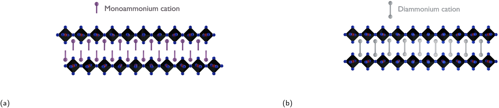 | ||
| Fig. 10 Illustration of (a) an RP phase with an eclipsed configuration and (b) a DJ phase with a staggered configuration. | ||
Ahmad and coworkers built DJ phase- and RP phase-based solar cells, the prior using 1,3-propanediammonium (PDA2+) and the latter using propylammonium (PA+).167 Fabricated under the same conditions, the RP phase-based solar cell displayed a PCE of 8.8%, whereas the solar cell with a DJ phase had a significantly higher PCE of 13.3%. The device with a PCE of 13.3% was built using a film of (PDA)(MA)3Pb4I13, which was deposited at a hot-casting temperature of 190 °C. Moreover, the unencapsulated device containing the DJ phase exhibited much higher stabilities compared to its RP phase counterpart. The group explained DJ phases to show enhanced material and device stability as a result of the elimination of the van der Waals gap that exists in RP phases.
Solar cell based on the DJ phase (3AMP)(MA0.75FA0.25)3Pb4I13, where 3AMP2+ is 3-aminomethylpiperidinium, was fabricated and displayed a champion PCE of 12.04%.168 The device exhibited superior air and light stability than 3D haloplumbate perovskites. It was shown that adding FA+ to MA+ until an FA+:MA+ ratio of 1:3 is attained increases the Pb–I–Pb angles, decreasing the electronic band gap and recombination rate, hence achieving higher fill factor (FF) and open current voltage (VOC). Moreover, it was also demonstrated for the DJ phase film using a mixture of N,N-dimethylformamide (DMF), dimethyl sulfoxide (DMSO), and hydriodic acid (HI) to yield better crystallinity and preferred vertical orientation growth.
A solar cell with an inverted structure based on the same compound (3AMP)(MA0.75FA0.25)3Pb4I13 was built, in which the photosensitizer layer was deposited using a deposition method combining both pre-annealing and merged annealing.169 In other words, the process involved the spin-coating of (3AMP)(MA0.75FA0.25)3Pb4I13, annealing of the DJ phase compound for a short period of time, spin-coating of the electron-transport material PC61BM, followed by another annealing step. The solar cell delivered a high PCE of 18.67% along with a VOC of 1.24 V.
Xu et al. introduced employing thieno[3,2-b]thiophene-2,5-diyldimethanammonium iodide (TTDMAI) as the spacer cation for DJ phases.171 The solar cell based on (TTDMA)MA3Pb4I13 displayed a superior PCE of 18.82% along with an exceptional stability. In fact, the unencapsulated device retained 99% of its original efficiency after being stored in an N2-filled glove box for 4400 h. The DJ phase film displayed good film quality and preferred vertical orientation, which are speculated to be as a result of the large crystal nuclei in the TTDMA–Pb precursor solution and the increased interlayer molecular interactions due to the extended π-conjugation length of the fused-thiophene group.
A NH4SCN additive was introduced to a series of DJ phases with the formula (XDA)(MA)n−1PbnI3n+1, where XDA2+ is p-xylylenediammonium.172 The 〈n〉 = 4 phase, (XDA)(MA)3Pb4I13, was shown to be the most optimal composition to be used as a PV device material due to its suitable band gap of 1.61 eV and better device efficiency. The optimized PV device of the abovementioned compound exhibited a stabilized PCE of 17.05% and also retained 80% of its initial efficiency after being exposed to 50% relative humidity for 1000 h when unencapsulated. Previously, other papers demonstrated that by introducing NH4+ and SCN− using NH4I and PbSCN as additives, one greatly improves film crystallization and reduces trap density, respectively.173,174 The addition of NH4+ slowed down crystal growth rate, whereas the inclusion of SCN− led to reduced trap density and enhanced intrinsic stability of the film. Adding both NH4+ and SCN− as additives by using NH4SCN during solution processing of (XDA)(MA)3Pb4I13 resulted in increased crystallinity, larger crystalline grains, reduction in film roughness, vertical-orientated films, reduced defect density, better carrier lifetime, and higher carrier mobility.
The effect of light illumination on the structure and charge carrier properties of the DJ phase (4AMP)(MA)2Pb3I10 was investigated by Mohite and coworkers.175 Using GIWAXS while continuously illuminating the sample for 51 min, a contraction of the lattice in the out-of-plane and in-plane directions by 1.0% and 0.56% was observed. XPS was carried out and suggested the oxidation of iodide ions. This can promote oxidative coupling of these ions across the interlayer, resulting in a contraction of the lattice structure. This reversible process, however, was not observed for the RP phase, (BA)2(MA)3Pb3I10, as a consequence of the longer interlayer distance. Notably, the contraction led to a sharp increase in charge carrier transport, open-circuit voltage, and fill factor of the DJ phase-based photovoltaic device, resulting in a PCE increase from 15.6 to 18.3%.
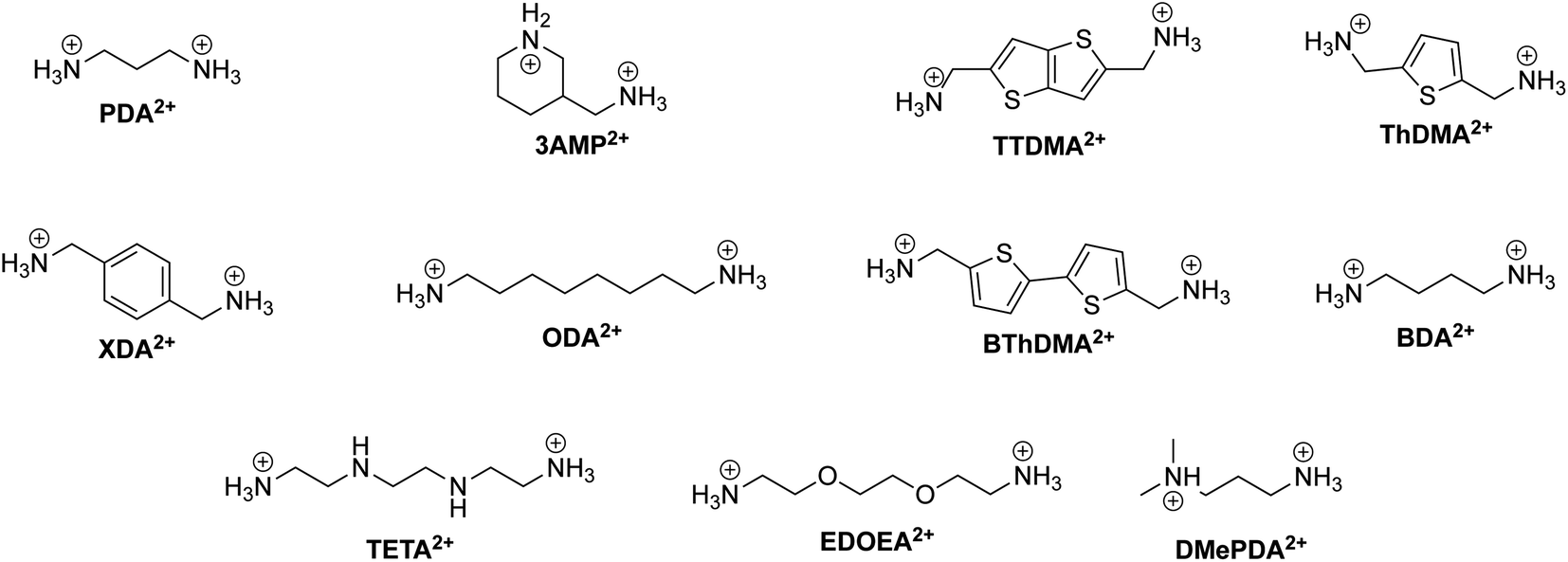
We present a table summarizing the recent progress of DJ phase-based solar cells in Table 4. The table includes information on the spacer cation, DJ phase composition, device structure, device performance, and stability of various DJ phase-based solar cells. This information is valuable for understanding the current state of the field and for informing future research efforts in developing more efficient and stable DJ phase-based solar cells. Additionally, the chemical structure of the diammonium organic spacers covered in this review are displayed in Fig. 11.
| Spacer cation | Composition | Device structure | PCE (%) | Stability | Ref. |
|---|---|---|---|---|---|
| a ST1: 4-(4-(bis(4-(4-(dibutylamino)styryl)phenyl)-amino)styryl)-N,N-dibutylaniline.210 | |||||
| 3-Aminomethylpiperidinium (3AMP2+) | (3AMP)(MA0.75FA0.25)3Pb4I13 | ITO/(NiOx/PTAA)/DJ phase/PC61BM/BCP/Ag | 18.67 | Unencapsulated device: 90% of initial PCE after 60 days of exposure to relative humidity of 45 ± 5% and 90% of initial PCE after 480 h of heating at 85 °C in N2 | 169 |
| Thieno[3,2-b]thiophene-2,5-diyldimethanammonium (TTDMA2+) | (TTDMA)(MA)3Pb4I13 | ITO/PEDOT:PSS/DJ phase/PC61BM/BCP/Ag | 18.82 | Unencapsulated device: 99% of initial PCE after 4400 h in N2, 94% of initial PCE after 740 h of light soaking in N2, 94% of initial PCE after 740 h of heating at 80 °C in N2, and 98% of initial PCE after 960 h of exposure to relative humidity of 30 ± 5% | 171 |
| Thiophene-2,5-diyldimethanammonium (ThDMA2+) | (ThDMA)(MA)3Pb4I13 | ITO/PEDOT:PSS/DJ phase/PC61BM/BCP/Ag | 15.32 | Unencapsulated device: 96% of initial PCE after 4400 h in N2, 88% of initial PCE after 740 h of light soaking in N2, 89% of initial PCE after 740 h of heating at 80 °C in N2, and 95% of initial PCE after 960 h of exposure to relative humidity of 30 ± 5% | 171 |
| (ThDMA)(MA)4Pb5I16 | ITO/PEDOT:PSS/DJ phase/PC61BM/BCP/Ag | 15.75 | Unencapsulated device: 95% of initial PCE after 1655 h of storage in N2 environment at room temperature and 88% of initial PCE after 668 h of continuous light soaking at 100 mW cm−2 in N2 environment at room temperature | 205 | |
| p-Xylylenediammonium (XDA2+) | (XDA)(MA)3Pb4I13 | FTO/c-TiO2/SnO2/DJ phase/spiro-OMeTAD/Au | 17.05 | Unencapsulated device: 80% of initial PCE after 1000 h after exposure to relative humidity of 50% at ambient temperature and 76% of initial PCE after 200 h of heating at 85 °C | 172 |
| 1,3-Propanediammonium (PDA2+) | (PDA)(Cs0.05MA0.95)3Pb4I13 | FTO/SnO2/DJ phase/spiro-OMeTAD/Au | 18.30 | Unencapsulated device: 93% of initial PCE after 1000 h of 1 sun illumination at maximum power point, 96% of initial PCE after 240 h of exposure to relative humidity of 85% and heat at 85 °C | 206 |
| 1,4-Butanediammonium (BDA2+) | (BDA)(MA)4Pb5I16 | ITO/PTAA/DJ phase/PC61BM/BCP/Ag | 16.19 | Unencapsulated device: 83.6% of initial PCE after 700 h of continuous illumination at 100 mW cm−2 and no loss in efficiency after 3 months of storage in N2 environment | 207 |
| (BDA)(Cs0.1FA0.9)4Pb5I16 | FTO/c-TiO2/m-TiO2/DJ phase/ST1/Cr/Au | 18.2 | Unencapsulated device: no loss in efficiency after 800 h of exposure to 80% relative humidity, over 80% of initial PCE after 800 h of heating at 85 °C, and over 90% of initial PCE after 800 h of continuous 1.1 sun illumination at 30 °C and relative humidity of 35% | 208 | |
| [2,2′-Bithiophene]-5,5′-diyldi-methanaminium (BThDMA2+) | (BThDMA)(MA)4Pb5I16 | ITO/PEDOT:PSS/DJ phase/PC61BM/BCP/Ag | 18.1 | Unencapsulated device: no loss in efficiency after 3100 h of storing in N2 environment and after 500 h of exposure to relative humidity of 30–50%. 82% of initial PCE after 300 h of heating at 85 °C | 209 |
 | ||
| Fig. 11 Chemical structure of relevant DJ phase organic spacer cations along with their abbreviations labeled in bold. | ||
3.8 DJ phase 2D/3D perovskite junction
Analogous to the concept described in Subsection 3.4, where the introduction of small quantities of monoammonium organic cation salt onto a 3D perovskite film results in the formation of an RP 2D/3D perovskite junction, substituting the monoammonium cation with a diammonium yields a DJ 2D/3D perovskite junction. The 2D layer between the 3D layer and the charge transport layer can help passivate defects and suppress non-radiative recombination loss at the interface surfaces, leading to both increased PCE and enhanced device stability. This is evidenced by several studies employing diverse diammonium spacer cations. For instance, in 2020 an unencapsulated solar cell with a DJ 2D/3D perovskite junction was successfully constructed and exhibited an impressive PCE of 21.6%.176 The active layers were fabricated by spin-coating (ODA)I2 (ODA2+ = octane-1,8-diammonium) onto a layer of (FA0.85MA0.15)Pb(I0.85Br0.15)3. A decreased hysteresis was observed and may be caused by the improved charge transport between the active layer and HTL layer and the large size of ODA2+ suppressing ion migration. To compare the stability of the DJ 2D/3D perovskite solar cell to that of the RP phase counterpart, a RP 2D/3D perovskite photovoltaic device using PEA+ as the spacer cation was constructed. After 360 h of exposure to a constant relative humidity of 85%, the device based on a DJ and RP layer retained 90 and 62% of its initial efficiency, respectively. This result emphasizes the importance of DJ phases and how simple substitution of the monoammonium cation with a diammonium cation within the 2D passivation layer can significantly enhance device stability.A photovoltaic device based on a 2D/3D structure using the same space cation, ODA2+, was reported.177 This time, a higher efficiency was achieved by adding (BA)I as a surface defect passivator, further improving phase stability of the film and device performance. The synergistic effect of (BA)I and (ODA)I2 led to formation of larger grains, reduced trap density of electrons and holes, and better crystallinity of the films. Furthermore, the PCE of a device with the additional DJ phase layer demonstrated a champion PCE of 22.19%.
To explore the impact of spacer cations on crystallization kinetics and carrier transport within DJ 2D/3D perovskite systems, three distinct spacer cations were incorporated into the 2D layer positioned above the (FA)PbI3 film.178 Among the studied cations, one is ODA2+, while the other two are TETA2+ and EDOEA2+, which are the oxidized forms of triethylenetetramine and 2,2′-(ethylenedioxy)bis(ethylamine), respectively. The latter two cations share structural similarities with ODA2+, except for the substitution of two carbon atoms in the linear aliphatic systems with either nitrogen or oxygen atoms. The work demonstrates how the identity of the organic cation affects hydrogen bonding and binding energy between the organic spacers and the inorganic layers, such that the perovskite crystals on the surface re-orientate themselves depending on the type of organic species used. Films containing EDOEA2+ exhibited fully vertically-oriented and the largest grains, showed almost no excess PbI2 nanosheets, and displayed improved properties such as suppressed non-radiative recombination, decreased defect densities, and longer charge carrier lifetime. Moreover, EDOEA2+ distributed in the grain boundaries greatly inhibited ion migration and at the same time enhanced moisture stability. The constructed solar cell containing EDOEA2+ demonstrated an impressive champion PCE of 22.68% and a high VOC of 1.15 V. The device retained 82% of its initial PCE after 1560 h of exposure to relative humidity of 50 ± 5%.
Since bonding strength between the spacer cation and the inorganic octahedra affects band offsets and weaker hydrogen bonding should improve hole transport, the use of an asymmetric bulky organic cation, DMePDA2+ (N,N-dimethyl-1,3-propane diammonium), was proposed.179 Due to the cation's asymmetric property, different configurations of (DMePDA)PbI4 can be obtained, with one of them being (DMePDA)PbI4-1 (stable polymorph) and the other being (DMePDA)PbI4-2 (metastable polymorph). The out-of-plane transport of (DMePDA)PbI4-2 was found to be approximately 4–5 times faster than its BDA2+-based counterpart. This enhancement is attributed to the reduction in energy barrier between the spacer cations and the inorganic layer. (DMePDA)I was deposited on top of triple cation perovskites of different compositions, with the formation of the metastable polymorph (DMePDA)PbI4-2 above the 3D structure. An impressive PCE of 24.7% was demonstrated using the metastable configuration as the passivation layer. Moreover, under a nitrogen atmosphere at 40 °C, the passivated device exhibited only a 10% drop in efficiency after 1000 h, while the control device experienced a more substantial decrease of 43% over the same duration.
Other examples of different spacer cations that had been explored, leading to improved performance and stability, include benzene-1,4-diammonium,180 1,4-phenylenedimethanammonium,181 hexane-1,6-diammonium,182 butane-1,4-diammonium,183 and 2,2′-disulfanediylbis(ethan-1-ammonium).184
3.9 DJ phases beyond photovoltaic application
While DJ phases demonstrate properties comparable to RP phases and exhibit enhanced stability as well as improved charge carrier transport in comparison, their potential for other optoelectronic applications, such as LEDs, remained largely unexplored until the past 2–3 years.185 The funneling mechanism facilitating an efficient charge transfer from wide band gap to narrow band gap emitters, reducing non-radiative recombination, is also observed in DJ phases.186 DJ phase-based LEDs have, despite receiving less research attention, caught up in EQEs with their RP phase counterpart. For instance, recent works have demonstrated sky-blue emitting LEDs utilizing DJ phases achieving EQEs surpassing 15%.187,188 One of the strategies is, as previously discussed, to modulate phase distribution. DMSO vapor treatment was shown to completely suppress the n = 1 phase and partially inhibit the formation of the n = 2 phase.187 This simple method was shown to effectively modulate the phase distribution due to the diammonium cations being able to migrate during the spin-coating process in the presence of DMSO vapor, such that the aggregation of diammonium cations is prevented. LED devices based on DJ phases that have undergone DMSO vapor treatment with emission peaks of 489 and 494 nm displayed an EQE of 13.7 and 15.5%, respectively.DJ phases have gained increased research attention in recent years for other optoelectronic avenues that have been previously investigated for RP phases. These areas include lasing,189 photodetection,190–194 radiation detection,195–198 scintillation,199 and memory applications.200
3.10 Challenges of organic spacer cations
Up to this point, we have examined various spacer cations and their implications, encompassing a range of effects such as phase purity, phase distribution, crystallite orientation, stability, charge carrier dynamics, and band offsets. Thus, it is evident that the design of the spacer cation plays a pivotal role for both device performance and device stability. Cation design includes introducing functional groups like fluoro- or thio-groups. The former can enhance film crystallinity and induces vertical orientation of the crystallites, while the latter can improve carrier transport properties by increasing intermolecular interactions between the spacer cations. Additionally, introducing an asymmetric bulky cation to form metastable polymorphs of the RP phase has been demonstrated to enhance device performance.While cation design is indeed important, it is imperative not to fixate solely on this aspect but to explore alternative methodologies. For instance, simple elimination of the van der Waals gap by introducing diammonium cations has proven to be advantageous for both device performance and stability. This prompts the question: is it possible to further modify the environment of the interlayer space as a whole? The short response to this question is “yes”. By introducing a phase similar to RP and DJ phases consisting of polymerized monoammonium or diammonium cations in the interlayer space, one can eliminate the gap between the “stacking” of the spacer groups. To end the section on CMHs with 2D structural dimensionality, we would like to briefly cover the aforementioned phase. A paper from 2021 reported the work on polymerized 4-vinylbenzylammonium in the interlayer space with increased lattice rigidity.201 The theoretically calculated crystal structure consisting of the polymerized 4-vinylbenzylammonium group is displayed in Fig. 12. From the figure it is evident that the structure, similar to RP phases, consists of an eclipsed configuration, but with the van der Waals gap eliminated. Furthermore, the monoammonium groups after polymerization are linked together via strong covalent bonds, resulting in overall increased structural rigidity and improved thermal stability. The system demonstrates enhanced carrier mobility and diminished non-radiative recombination, with the former linked to reduced phonon scattering and the latter linked to suppressed electron–phonon coupling. LED devices based on this polymerized phase exhibited EQEs of up to 23.2%. Other similar quantum well structures composed of polymerized organic networks in the interlayer have been studied and explored more in recent years.202–204 These novel phases, characterized by enhanced structural rigidity and improved stabilities, exhibit remarkable properties, making them formidable contenders to outperform both RP and DJ phases.
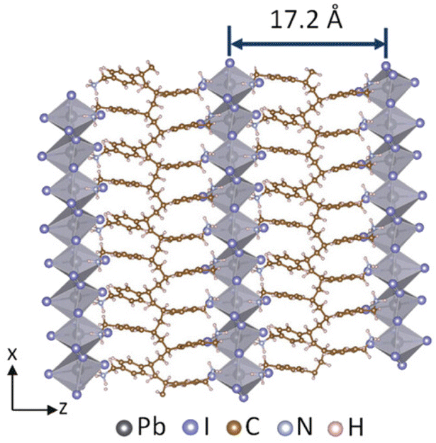 | ||
| Fig. 12 Calculated crystal structure of (PVBA)2PbI4 (PVBA+ = polymerized 4-vinylbenzylammonium). Reproduced with permission.201 Copyright 2021, John Wiley and Sons. | ||
4 CMH nanoplates/nanosheets
This section will give a brief overview of CMH nanoplates and nanosheets, focusing on the synthesis and structural properties of lead-based colloidal systems. For a comprehensive exploration of the optoelectronic characteristics of colloidal perovskite NPLs, we recommend delving into the review by Polavarapu et al.211 Colloidal CMH systems usually consist of ligands L with long organic chains, most commonly oleylammonium (OLA+) and oleic acid, that passivate the nanocrystal surface and prevent agglomeration due to the particle's high surface-area-to-volume ratio.211 Examples include CMH nanoplatelets (NPLs),212,213 nanowires,214–216 nanocubes,56 and quantum dots (QDs).217,218 Colloidal CMH NPLs possess the general formula L2[ABX3]p−1BX4, where p, analogous to m and n for RP and DJ phases, respectively, corresponds to the thickness of the octahedral layer (or in this case the nanocrystal thickness). By reducing the crystal size to a few unit cells in size and reducing the form factor dimensionality, one restricts the system's charge carrier movement and introduces quantum and dielectric confinement effects. The exciton Bohr radius of (MA)PbI3, the separation distance between the electron–hole pair, is around 2–3 nm.219,220 When the size of the nanostructure is larger than the exciton Bohr radius aB, the electron and hole pair can be described by a single wave function.221 In contrast, when the nanoparticle size is smaller than aB, the wave function of the electron and hole must be viewed separately. For the latter case the system experiences enhanced quantum confinement effects. Similar to the previously discussed groups with a structural dimensionality of 2, for which the optoelectronic properties can be tuned by varying the well width, the absorption onset and PL of an NPL can both be tuned by varying the NPL's thickness.A major advantage that colloidal CMH NPLs offer is the control of their synthesis. For instance, the control of the size of lead-based colloidal CMH nanocubes below 4 nm is rather challenging. Consequently, these usually show weaker quantum confinement effects.217,222 By contrast, one can synthesize colloidal CMH NPLs with its width being less than 4 nm more easily.223 A sharp blue-shift in excitonic absorption was observed in NPLs with predominantly single cell thickness containing corner-sharing PbBr6 octahedra when compared to bulk 3D (MA)PbBr3.224 CMH NPLs generally have an increased exciton binding energy, narrow emission peaks, blue-shift in absorption onset, and a shortened fluorescent decay time compared to their bulk 3D counterparts.225,226 Lead-based CMH nanosheets and NPLs have demonstrated their suitability for LED application, as well as their potential as candidates for nanolasing,227 scintillators,228 and photocatalysts for CO2 reduction.229
In 2014, a nanometer-thin layer of (MA)PbBr3 was shown to exhibit high quantum efficiencies and demonstrated its potential for cost-effective display, lighting, and optical communication applications, thereby stimulating a substantial increase in research attention towards lead-based CMHs for LED applications.22 The publication of several notable papers on CMH nanocrystals, including NPLs, contributed to an increased interest in conducting research on these materials in 2015. The following will give a brief overview of some notable works published in that year.
Hot-injection (HI) method was used to synthesized monodisperse colloidal CsPbX3 (X = Cl−, Br−, I−) nanocubes by Protesescu and coworkers in 2015.56 The HI technique involves injecting a Cs-oleate solution into a hot solution containing PbX2 and 1-octadecene in an inert environment. This is followed by quenching of the reaction with an ice bath almost immediately after injection. The group demonstrated the facile synthesis of the nanocubes with sizes between 4 and 15 nm by simply varying the reaction temperature. In the same year, ligand-assisted reprecipitation (LARP) method was introduced by Zhang et al.217 The group synthesized brightly luminescent colloidal CsPbX3 (X = Cl−, Br−, I−) QDs with a PQLY of up to 70%. The LARP technique consists of mixing CMH precursors in a good solvent into a vigorously stirring bad solvent that comprises capping ligands possessing extended organic chains. Currently, LARP method, alongside HI method, are two of the most commonly used techniques to synthesize colloidal CMH nanocrystals, including CMH NPLs.
The first CMH NPL, which is based on CsPbX3 (X = Cl−, Br−, I−), was also reported in 2015.230,231 NPLs with thicknesses between 1 and 5 unit cells were synthesized using HI method and displayed high PLQYs of up to 84.4%. The trick here was to inject the Cs-oleate solution at elevated temperatures. In the same year, another group demonstrated the synthesis of CMH NPLs using LARP technique.232 It was demonstrated that the thickness of NPLs with a lead bromide framework containing organic ligands octylammonium (OA+) and MA+ can be tuned by varying the ratio of the organic cations. Purely using OA+ with complete absence of MA+ leads to the formation of one unit cell thick nanoplatelets that have a PL emission of 427 nm. Introducing MA+, i.e., increasing the MA+:OA+ ratio, increases the NPL thickness, thereby red-shifting both the absorption onset and PL. SEM images showed the platelets to be stacked on top of each other. The hybridization of the wavefunction of the electrons and holes with those of adjacent NPLs leads to minibands being formed.232
Through hot-injection method, the role of acid–base equilibria of CsPbBr3 nanocrystals using oleylamine and oleic acid was explored. CMH NPLs were synthesized at higher temperatures (around 195 °C) than previously reported synthesis conditions,230,236 and they were shown to be able to be synthesized by simply reducing the oleic acid concentration in both the reaction mixture.237 Additionally, the thickness of the NPL can be varied by reducing the concentration of Cs+. This was demonstrated in different temperature conditions. In another paper, the effect of hydrocarbon chain length of the acid and base on the shape and size of the nanocrystal was shown.236 Decreasing the chain length of the amine and working at a lower temperature of 140 °C enables the formation of thinner NPLs.
Single and few-unit-cell-thick BA2PbBr4 nanosheets were synthesized via solution-phase growth by employing a ternary co-solvent consisting of chlorobenzene, DMF, and acetonitrile.238 BA2PbBr4 nanosheets crystallized after dropping a very dilute solution of its precursors into a Si/SiO2 substrate surface and drying it under moderate heating. The thinnest sheets were found to be approximately 1.6 nm, while their PLQY was calculated to be around 26%.
Two-step synthesis of lead-based CMH nanosheets involves the formation of PbX2 nanosheets followed by the conversion to the CMH structure with usually MAI. Zheng and coworkers demonstrated a two-step method to synthesize free-standing (MA)PbBr3 nanosheets that are around 1 cm in lateral size and 100 nm in thickness, involving the synthesis of PbBr2 nanosheets in solution via a reprecipitation method, followed by the conversion to the CMH using MABr vapor via a vapor–solid reaction.239 Using two-step synthesis, (MA)PbI3 nanosheets as thin as a single unit cell were synthesized by Liu et al.240 The synthesis consisted of solution processing of PbI2 followed by the conversion to (MA)PbI3 nanosheets using a CVD setup. The key to obtaining large quantities of nanosheets was shown to lie in the control of the heating during the solution process. Elevating the temperature of aqueous PbI2 on a SiO2/Si substrate to not higher than 90 °C leads to the formation of more nanosheets. However, the slow crystal growth process at lower heating temperatures affects the crystal structure, resulting in low PL intensities.
It was recently reported that two-monolayer thick CsPbBr3 NPL superlattices with either a face-down or an edge-up configuration can be assembled via HI method by controlling the evaporation rate of the dispersion solvent.233Fig. 13a shows the two different configurations, how each configuration can be achieved by controlling the evaporation rate, and the scanning transmission electron microscopy (STEM) images of the two superlattice assemblies. The group demonstrated how fast evaporation of the solvent leads to the kinetically trapped state, which is the face-down configuration, whereby slow solvent evaporation results in the edge-up orientation, the more thermodynamically favored state. The NPLs in both configurations have face-to-face stacking and possess lateral dimensions of 15 nm. Moreover, the edge-up orientation had a significantly higher polarization factor of 0.29 compared to the face-down orientation's polarization factor of 0.04. This is due to the transition dipoles in the edge-up orientation pointing along the long axis of the NPLs, while the face-down orientation has a two-dimensional degeneracy in the plane of the NPLs. The study also shows that, when decreasing the temperature from 298 to 258 K, the face-down NPL assembly exhibits a rare uniaxial negative thermal expansion (NTE) effect, whereby the NPLs experience a decrease in lead–lead distance along the axial axis. Stacked colloidal perovskite nanoplatelets, such as the edge-up superlattices in Fig. 13a with a F2S3 dimensionality, share structural similarities with RP phases with a dimensionality of F3S2. The identification and classification of such nanoplatelets can be effectively achieved by comparing their X-ray diffraction (XRD) pattern with those of perovskites and RP phases. For instance, the XRD pattern of the edge-up superlattice in Fig. 13b displays characteristic peaks of bulk CsPbBr3 as shown in Fig. 13c. The additional peaks from the face-down superlattice arise from the ordering of the nanoplatelets and are distinctly different from the XRD pattern of typical RP phases as seen in Fig. 13d, which provides the XRD pattern of several RP phases with different m values. It can be extracted from Fig. 13d that the diffractograms of (BA)2(MA)m−1PbmI3m+1 (m = 2, 3, 4) are primarily defined by the (0k0) and (111) reflection planes in the lower 2θ regions, where (0k0) is the plane parallel to the inorganic layer. Simulated XRD data of Cs2Pbl4 for m = 1 using VESTA is used, since no data of (BA)2PbI4 (m = 1) was available on ICSD at the time of writing this review. After comparing the XRD data of the superlattice to that of CsPbBr3 and several RP phases, and confirming that the XRD pattern of RP phases do not match the XRD data of the superlattice, we can conclude that the assembly of superlattices can be categorized as perovskites.
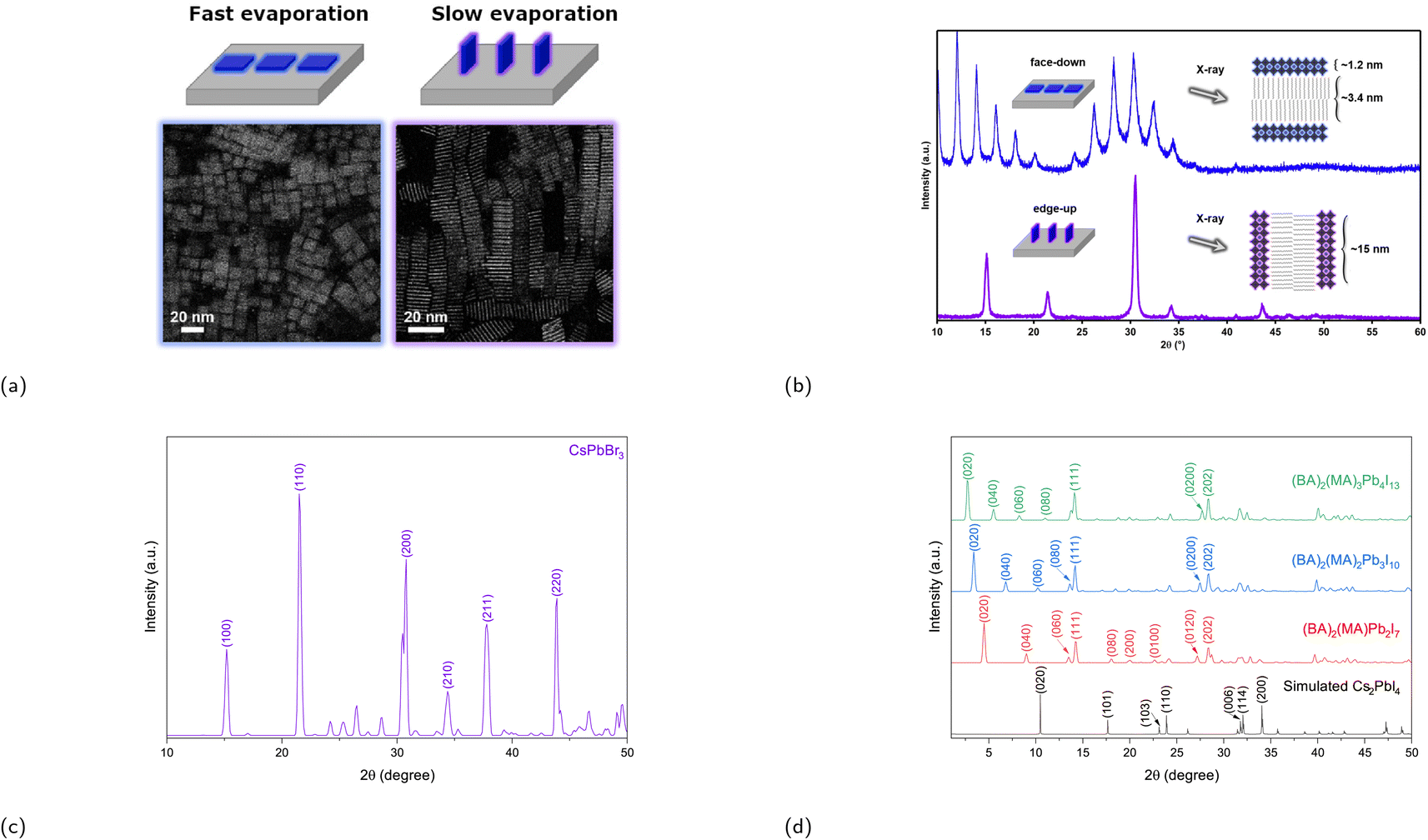 | ||
| Fig. 13 (a) Illustration of face-down (left) and edge-up (right) assemblies through varying the evaporation rate of the dispersion solvent. The STEM images of each assembly is shown at the bottom. (b) XRD diffraction patterns of the face-down (top) and edge-up (bottom) superlattices. Reproduced with permission.233 Copyright 2023, American Chemical Society. XRD patterns of (c) CsPbBr3 and (d) four different RP phases are attained from the ICSD database (λ = 1.5418 nm).234,235 | ||
Recently, a multi-amine chelating ligand, namely N′-(2-aminoethyl)-N′-hexadecylethane-1,2-diamine (AHDA), was used to synthesize CsPbI3 nanocrystals.241 The protonated diammonium ligand can bind itself to the perovskite nanoparticle surface with a binding energy of 2.36 eV, which is 0.89 eV higher than the binding energy achieved when using oleylammonium. The use of the proposed ligand suppresses dynamic desorption of the ligands and provides enhanced stability of the nanocrystal. It was also shown that the ligand can be used to synthesize other perovskite nanocrystals with the composition CsPbCl3, CsPbBr3, CsPbBrI2, and (FA)PbI3. This discovery holds significance as it implies the existence of undiscovered ligands that can enhance the charge-transfer properties of perovskite nanocrystals for use in photocatalytic and optoelectronic applications.
5 Conclusions and perspectives
In this review, we first introduced the composition-based term ‘complex metal halides’, CMHs in short, to classify compounds such as halide perovskites that have emerged as a highly promising class of materials for next-generation solar cells. CMHs, based on the term ‘complex metal oxides’, include a wide variety of compounds, such as (MA)2KBiCl6, Cs2InAg6, and 2D halide-based Ruddlesden–Popper phases. The act of introducing this term helps avoid current inconsistencies associated with the usage of the term ‘perovskite’, especially for structures that are not resemblant to the perovskite aristotype. We then presented a classification table allocating CMHs based on their structural and form factor dimensionality. It was extracted from the table that most CMH research to date has been on bulk 3D perovskites, with many of the lower-dimensional avenues being under-explored. The promising potential demonstrated by the relatively unexplored areas for optoelectronic applications coupled with the recent trend seen in the shift in research focus from 3D to 2D materials suggests that there will be a surge in research efforts directed towards these areas in the future. Decreasing form factor or structural dimensionality (or both) results in enhanced quantum and dielectric confinement effects, increasing the exciton binding energy, lowering the electronic and optical band gap, and thereby inducing both a blue-shift in absorption and photoluminescence of the system. These effects and properties are observed in Ruddlesden–Popper (RP) phases and Dion–Jacobson (DJ) phases, both of which have been extensively covered in this review. We delved into notable discoveries regarding the application of these materials in light-harvesting and light-emitting contexts. Specifically, we examined the impact of cation engineering, exploring their roles in enhancing both device performance and stability. Moreover, the integration of RP/DJ phases with 3D perovskites such as (MA)PbI3 to improve device performance and stability was also reviewed. In the final section of this review, we delved into the synthesis of colloidal perovskite nanoplatelets, accompanied by a brief analysis of their structural characteristics.The utilization of perovskites as wide band gap semiconductors for photovoltaics is promising, particularly in the context of multi-junction tandem solar cells. When constructing tandem cells consisting of Si bottom cells with perovskite top cells, it becomes possible to surpass the Shockley–Queisser limit. This, in turn, plays a pivotal role in advancing the commercialization prospects of perovskite-based technologies. Despite these promising attributes, perovskites face stability issues that need to be overcome.242 Addressing this concern, researchers have explored the passivation of perovskite layers using lower-dimensional compounds such as RP and DJ phases, which consist of hydrophobic spacer cations. This approach has demonstrated the potential to significantly improve the operational stability of perovskite solar cells. However, the progress made in stability enhancement still falls short of the requirements outlined by international standards (IEC 61646). While this review predominantly delves into the functional aspects of lead-based systems, it is crucial to acknowledge that numerous lower-dimensional, non-toxic, lead-free alternatives have yet to be fully explored. Presently, devices based on lead-free systems lag behind their lead counterparts in terms of device performance. The question arises: can lead-free CMHs eventually match or surpass the extensively studied lead derivatives in terms of device performance? Notably, the replacement of lead holds promise not only in terms of environmental concerns but also for enhancing the commercial viability of these systems. Further research and development in both lead-free and lead-based CMHs are imperative to achieve the necessary device performance as well as durability for the widespread commercialization of CMH for various optoelectronic applications including photovoltaics, LEDs, lasing, and photodetectors.
Author contributions
All authors contributed to writing this manuscript.Conflicts of interest
There are no conflicts to declare.Acknowledgements
This work was supported by the Agriculture Program of the Agency for Science, Technology and Research (A*STAR) (Grant No. A19D9a0096).Notes and references
- M. Chhowalla, H. S. Shin, G. Eda, L.-J. Li, K. P. Loh and H. Zhang, Nat. Chem., 2013, 5, 263–275 CrossRef PubMed.
- L. Maggini and R. R. Ferreira, J. Mater. Chem. C, 2021, 9, 15721–15734 RSC.
- R. H. Mitchell, M. D. Welch and A. R. Chakhmouradian, Mineral. Mag., 2017, 81, 411–461 CrossRef CAS.
- G. Rose, J. Prakt. Chem., 1840, 19(1), 459–468 CrossRef.
- H. L. Wells, Z. Anorg. Chem., 1893, 3, 195–210 CrossRef.
- A. Kojima, K. Teshima, Y. Shirai and T. Miyasaka, J. Am. Chem. Soc., 2009, 131, 6050–6051 CrossRef CAS PubMed.
- NREL, Best Research-Cell Efficiencies, 2023 Search PubMed.
- A. K. Jena, A. Kulkarni and T. Miyasaka, Chem. Rev., 2019, 119, 3036–3103 CrossRef CAS PubMed.
- M. A. Green, A. Ho-Baillie and H. J. Snaith, Nat. Photonics, 2014, 8, 506–514 CrossRef CAS.
- S. D. Stranks, G. E. Eperon, G. Grancini, C. Menelaou, M. J. Alcocer, T. Leijtens, L. M. Herz, A. Petrozza and H. J. Snaith, Science, 2013, 342, 341–344 CrossRef CAS PubMed.
- D. W. de Quilettes, S. M. Vorpahl, S. D. Stranks, H. Nagaoka, G. E. Eperon, M. E. Ziffer, H. J. Snaith and D. S. Ginger, Science, 2015, 348, 683–686 CrossRef CAS PubMed.
- A. Extance, Nature, 2019, 570, 429–432 CrossRef CAS PubMed.
- B. Conings, J. Drijkoningen, N. Gauquelin, A. Babayigit, J. D'Haen, L. D'Olieslaeger, A. Ethirajan, J. Verbeeck, J. Manca and E. Mosconi, et al. , Adv. Energy Mater., 2015, 5, 1500477 CrossRef.
- N.-K. Kim, Y. H. Min, S. Noh, E. Cho, G. Jeong, M. Joo, S.-W. Ahn, J. S. Lee, S. Kim and K. Ihm, et al. , Sci. Rep., 2017, 7, 4645 CrossRef PubMed.
- L. Ma, D. Guo, M. Li, C. Wang, Z. Zhou, X. Zhao, F. Zhang, Z. Ao and Z. Nie, Chem. Mater., 2019, 31, 8515–8522 CrossRef CAS.
- G. E. Eperon, S. D. Stranks, C. Menelaou, M. B. Johnston, L. M. Herz and H. J. Snaith, Energy Environ. Sci., 2014, 7, 982–988 RSC.
- S. N. Habisreutinger, T. Leijtens, G. E. Eperon, S. D. Stranks, R. J. Nicholas and H. J. Snaith, Nano Lett., 2014, 14, 5561–5568 CrossRef CAS PubMed.
- J. H. Noh, S. H. Im, J. H. Heo, T. N. Mandal and S. I. Seok, Nano Lett., 2013, 13, 1764–1769 CrossRef CAS PubMed.
- M. Ouafi, B. Jaber, L. Atourki, R. Bekkari and L. Laânab, J. Alloys Compd., 2018, 746, 391–398 CrossRef CAS.
- M. Benavides-Garcia and K. Balasubramanian, J. Chem. Phys., 1994, 100, 2821–2830 CrossRef CAS.
- R. K. Misra, S. Aharon, B. Li, D. Mogilyansky, I. Visoly-Fisher, L. Etgar and E. A. Katz, J. Phys. Chem. Lett., 2015, 6, 326–330 CrossRef CAS PubMed.
- Z.-K. Tan, R. S. Moghaddam, M. L. Lai, P. Docampo, R. Higler, F. Deschler, M. Price, A. Sadhanala, L. M. Pazos and D. Credgington, et al. , Nat. Nanotechnol., 2014, 9, 687–692 CrossRef CAS PubMed.
- H. Zhu, Y. Fu, F. Meng, X. Wu, Z. Gong, Q. Ding, M. V. Gustafsson, M. T. Trinh, S. Jin and X. Zhu, Nat. Mater., 2015, 14, 636–642 CrossRef CAS PubMed.
- G. Xing, N. Mathews, S. S. Lim, N. Yantara, X. Liu, D. Sabba, M. Grätzel, S. Mhaisalkar and T. C. Sum, Nat. Mater., 2014, 13, 476–480 CrossRef CAS PubMed.
- C. C. Stoumpos, C. D. Malliakas, J. A. Peters, Z. Liu, M. Sebastian, J. Im, T. C. Chasapis, A. C. Wibowo, D. Y. Chung and A. J. Freeman, et al. , Cryst. Growth Des., 2013, 13, 2722–2727 CrossRef CAS.
- M. I. Saidaminov, V. Adinolfi, R. Comin, A. L. Abdelhady, W. Peng, I. Dursun, M. Yuan, S. Hoogland, E. H. Sargent and O. M. Bakr, Nat. Commun., 2015, 6, 1–7 Search PubMed.
- S. Hu, Z. Ren, A. B. Djurišić and A. L. Rogach, ACS Energy Lett., 2021, 6, 3882–3905 CrossRef CAS.
- T. Ye, X. Wang, X. Li, A. Q. Yan, S. Ramakrishna and J. Xu, J. Mater. Chem. C, 2017, 5, 1255–1260 RSC.
- X. Li, F. Zhang, J. Wang, J. Tong, T. Xu and K. Zhu, Nat. Sustain., 2021, 4, 1038–1041 CrossRef.
- F. Corsini and G. Griffini, J. Phys.: Energy, 2020, 2, 031002 CAS.
- M. Pitaro, E. K. Tekelenburg, S. Shao and M. A. Loi, Adv. Mater., 2022, 34, 2105844 CrossRef CAS PubMed.
- H.-H. Fang, S. Adjokatse, S. Shao, J. Even and M. A. Loi, Nat. Commun., 2018, 9, 1–8 CrossRef PubMed.
- L. Chouhan, S. Ghimire, C. Subrahmanyam, T. Miyasaka and V. Biju, Chem. Soc. Rev., 2020, 49, 2869–2885 RSC.
- B.-B. Yu, Z. Chen, Y. Zhu, Y. Wang, B. Han, G. Chen, X. Zhang, Z. Du and Z. He, Adv. Mater., 2021, 33, 2102055 CrossRef CAS PubMed.
- R. L. Hoye, J. Hidalgo, R. A. Jagt, J.-P. Correa-Baena, T. Fix and J. L. MacManus-Driscoll, Adv. Energy Mater., 2022, 12, 2100499 CrossRef CAS.
- B. Saparov, F. Hong, J.-P. Sun, H.-S. Duan, W. Meng, S. Cameron, I. G. Hill, Y. Yan and D. B. Mitzi, Chem. Mater., 2015, 27, 5622–5632 CrossRef CAS.
- J. Breternitz and S. Schorr, Adv. Energy Mater., 2018, 8, 1802366 CrossRef.
- Q. A. Akkerman and L. Manna, ACS Energy Lett., 2020, 5, 604–610 CrossRef CAS PubMed.
- C. N. R. Rao and J. Gopalakrishnan, Acc. Chem. Res., 1987, 20, 228–235 CrossRef CAS.
- L. Katz and R. Ward, Inorg. Chem., 1964, 3, 205–211 CrossRef CAS.
- J. Li, C. Lin, Y. Min, Y. Yuan, G. Li, S. Yang, P. Manuel, J. Lin and J. Sun, J. Am. Chem. Soc., 2019, 141, 4990–4996 CrossRef CAS.
- M. I. Saidaminov, O. F. Mohammed and O. M. Bakr, ACS Energy Lett., 2017, 2, 889–896 CrossRef CAS.
- T. Jun, T. Handa, K. Sim, S. Iimura, M. Sasase, J. Kim, Y. Kanemitsu and H. Hosono, APL Mater., 2019, 7, 111113 CrossRef.
- F. Wei, Z. Deng, S. Sun, F. Xie, G. Kieslich, D. M. Evans, M. A. Carpenter, P. D. Bristowe and A. K. Cheetham, Mater. Horiz., 2016, 3, 328–332 RSC.
- G. Volonakis, A. A. Haghighirad, R. L. Milot, W. H. Sio, M. R. Filip, B. Wenger, M. B. Johnston, L. M. Herz, H. J. Snaith and F. Giustino, J. Phys. Chem. Lett., 2017, 8, 772–778 CrossRef CAS PubMed.
- Z. Xiao, W. Meng, J. Wang, D. B. Mitzi and Y. Yan, Mater. Horiz., 2017, 4, 206–216 RSC.
- X.-G. Zhao, D. Yang, J.-C. Ren, Y. Sun, Z. Xiao and L. Zhang, Joule, 2018, 2, 1662–1673 CrossRef CAS.
- M. I. Saidaminov, J. Almutlaq, S. Sarmah, I. Dursun, A. A. Zhumekenov, R. Begum, J. Pan, N. Cho, O. F. Mohammed and O. M. Bakr, ACS Energy Lett., 2016, 1, 840–845 CrossRef CAS.
- K. Ahmad, S. N. Ansari, K. Natarajan and S. M. Mobin, ACS Appl. Energy Mater., 2018, 1, 2405–2409 CrossRef CAS.
- A. K. Cheetham, C. Rao and R. K. Feller, Chem. Commun., 2006, 4780–4795 RSC.
- R. F. Pierret, Semiconductor Device Fundamentals, Pearson Education India, 1996 Search PubMed.
- X. Chen, H. Lu, Y. Yang and M. C. Beard, J. Phys. Chem. Lett., 2018, 9, 2595–2603 CrossRef CAS PubMed.
- A. Miyata, A. Mitioglu, P. Plochocka, O. Portugall, J. T.-W. Wang, S. D. Stranks, H. J. Snaith and R. J. Nicholas, Nat. Phys., 2015, 11, 582–587 Search PubMed.
- J. S. Manser and P. V. Kamat, Nat. Photonics, 2014, 8, 737–743 CrossRef CAS.
- A. Swarnkar, R. Chulliyil, V. K. Ravi, M. Irfanullah, A. Chowdhury and A. Nag, Angew. Chem., 2015, 127, 15644–15648 CrossRef.
- L. Protesescu, S. Yakunin, M. I. Bodnarchuk, F. Krieg, R. Caputo, C. H. Hendon, R. X. Yang, A. Walsh and M. V. Kovalenko, Nano Lett., 2015, 15, 3692–3696 CrossRef CAS PubMed.
- X. Li, Y. Wu, S. Zhang, B. Cai, Y. Gu, J. Song and H. Zeng, Adv. Funct. Mater., 2016, 26, 2435–2445 CrossRef CAS.
- V. V. Dutt, S. Akhil, R. Singh, M. Palabathuni and N. Mishra, J. Phys. Chem. C, 2022, 126, 9502–9508 CrossRef CAS.
- Y. Li, M. Cai, M. Shen, Y. Cai and R.-J. Xie, J. Mater. Chem. C, 2022, 10, 8356–8363 RSC.
- Y. Zhang, M. I. Saidaminov, I. Dursun, H. Yang, B. Murali, E. Alarousu, E. Yengel, B. A. Alshankiti, O. M. Bakr and O. F. Mohammed, J. Phys. Chem. Lett., 2017, 8, 961–965 CrossRef CAS.
- Y. Kim, E. Yassitepe, O. Voznyy, R. Comin, G. Walters, X. Gong, P. Kanjanaboos, A. F. Nogueira and E. H. Sargent, ACS Appl. Mater. Interfaces, 2015, 7, 25007–25013 CrossRef CAS.
- V. M. Goldschmidt, Sci. Nat., 1926, 14, 477–485 CrossRef CAS.
- W. Travis, E. Glover, H. Bronstein, D. Scanlon and R. Palgrave, Chem. Sci., 2016, 7, 4548–4556 RSC.
- D. B. Mitzi, J. Chem. Soc., Dalton Trans., 2001, 1–12 RSC.
- R. L. Milot, R. J. Sutton, G. E. Eperon, A. A. Haghighirad, J. M. Hardigree, L. Miranda, H. J. Snaith, M. B. Johnston and L. M. Herz, Nano Lett., 2016, 16, 7001–7007 CrossRef CAS PubMed.
- T. Ishihara, J. Takahashi and T. Goto, Phys. Rev. B: Condens. Matter Mater. Phys., 1990, 42, 11099 CrossRef CAS PubMed.
- E. Hanamura, N. Nagaosa, M. Kumagai and T. Takagahara, Mater. Sci. Eng., B, 1988, 1, 255–258 CrossRef.
- D. B. Straus and C. R. Kagan, J. Phys. Chem. Lett., 2018, 9, 1434–1447 CrossRef CAS PubMed.
- C. C. Stoumpos, C. M. M. Soe, H. Tsai, W. Nie, J.-C. Blancon, D. H. Cao, F. Liu, B. Traoré, C. Katan and J. Even, et al. , Chem, 2017, 2, 427–440 CAS.
- D. H. Cao, C. C. Stoumpos, O. K. Farha, J. T. Hupp and M. G. Kanatzidis, J. Am. Chem. Soc., 2015, 137, 7843–7850 CrossRef CAS PubMed.
- D. B. Mitzi, Prog. Inorg. Chem., 1999, 1–121 CAS.
- H. Mathieu, P. Lefebvre and P. Christol, Phys. Rev. B: Condens. Matter Mater. Phys., 1992, 46, 4092 CrossRef PubMed.
- G. Lanty, K. Jemli, Y. Wei, J. Leymarie, J. Even, J.-S. Lauret and E. Deleporte, J. Phys. Chem. Lett., 2014, 5, 3958–3963 CrossRef CAS PubMed.
- J.-T. Lin, C.-C. Liao, C.-S. Hsu, D.-G. Chen, H.-M. Chen, M.-K. Tsai, P.-T. Chou and C.-W. Chiu, J. Am. Chem. Soc., 2019, 141, 10324–10330 CrossRef CAS PubMed.
- A. Z. Chen, M. Shiu, J. H. Ma, M. R. Alpert, D. Zhang, B. J. Foley, D.-M. Smilgies, S.-H. Lee and J. J. Choi, Nat. Commun., 2018, 9, 1–7 CrossRef PubMed.
- Z. Wang, Q. Wei, X. Liu, L. Liu, X. Tang, J. Guo, S. Ren, G. Xing, D. Zhao and Y. Zheng, Adv. Funct. Mater., 2021, 31, 2008404 CrossRef CAS.
- K. Tanaka and T. Kondo, Sci. Technol. Adv. Mater., 2003, 4, 599–604 CrossRef CAS.
- K. Tanaka, T. Takahashi, T. Kondo, T. Umebayashi, K. Asai and K. Ema, Phys. Rev. B: Condens. Matter Mater. Phys., 2005, 71, 045312 CrossRef.
- X. Zhong, X. Ni, S. Sidhik, H. Li, A. D. Mohite, J.-L. Brédas and A. Kahn, Adv. Energy Mater., 2022, 12, 2202333 CrossRef CAS.
- M. C. Gélvez-Rueda, E. M. Hutter, D. H. Cao, N. Renaud, C. C. Stoumpos, J. T. Hupp, T. J. Savenije, M. G. Kanatzidis and F. C. Grozema, J. Phys. Chem. C, 2017, 121, 26566–26574 CrossRef PubMed.
- A. Caiazzo and R. A. Janssen, Adv. Energy Mater., 2022, 12, 2202830 CrossRef CAS.
- H. Tsai, W. Nie, J.-C. Blancon, C. C. Stoumpos, R. Asadpour, B. Harutyunyan, A. J. Neukirch, R. Verduzco, J. J. Crochet and S. Tretiak, et al. , Nature, 2016, 536, 312–316 CrossRef CAS PubMed.
- H. Ren, S. Yu, L. Chao, Y. Xia, Y. Sun, S. Zuo, F. Li, T. Niu, Y. Yang and H. Ju, et al. , Nat. Photonics, 2020, 14, 154–163 CrossRef CAS.
- C. Liang, H. Gu, Y. Xia, Z. Wang, X. Liu, J. Xia, S. Zuo, Y. Hu, X. Gao and W. Hui, et al. , Nat. Energy, 2021, 6, 38–45 CrossRef CAS.
- Z. He, Y. Zhou, C. Xu, Y. Su, A. Liu, Y. Li, L. Gao and T. Ma, J. Phys. Chem. C, 2021, 125, 16428–16434 CrossRef CAS.
- M. Shao, T. Bie, L. Yang, Y. Gao, X. Jin, F. He, N. Zheng, Y. Yu and X. Zhang, Adv. Mater., 2022, 34, 2107211 CrossRef CAS PubMed.
- K.-z. Du, Q. Tu, X. Zhang, Q. Han, J. Liu, S. Zauscher and D. B. Mitzi, Inorg. Chem., 2017, 56, 9291–9302 CrossRef CAS PubMed.
- S. Zhang, S. M. Hosseini, R. Gunder, A. Petsiuk, P. Caprioglio, C. M. Wolff, S. Shoaee, P. Meredith, S. Schorr and T. Unold, et al. , Adv. Mater., 2019, 31, 1901090 CrossRef PubMed.
- C. Ma, C. Leng, Y. Ji, X. Wei, K. Sun, L. Tang, J. Yang, W. Luo, C. Li and Y. Deng, et al. , Nanoscale, 2016, 8, 18309–18314 RSC.
- S. Jeong, S. Seo, H. Yang, H. Park, S. Shin, H. Ahn, D. Lee, J. H. Park, N.-G. Park and H. Shin, Adv. Energy Mater., 2021, 11, 2102236 CrossRef CAS.
- S. Sidhik, Y. Wang, M. De Siena, R. Asadpour, A. J. Torma, T. Terlier, K. Ho, W. Li, A. B. Puthirath and X. Shuai, et al. , Science, 2022, 377, 1425–1430 CrossRef CAS PubMed.
- K. Wang, Z.-Y. Lin, Z. Zhang, L. Jin, K. Ma, A. H. Coffey, H. R. Atapattu, Y. Gao, J. Y. Park and Z. Wei, et al. , Nat. Commun., 2023, 14, 397 CrossRef CAS PubMed.
- L. N. Quan, Y. Zhao, F. P. G. de Arquer, R. Sabatini, G. Walters, O. Voznyy, R. Comin, Y. Li, J. Z. Fan and H. Tan, et al. , Nano Lett., 2017, 17, 3701–3709 CrossRef CAS PubMed.
- M. E. Bouduban, V. I. Queloz, V. M. Caselli, K. T. Cho, A. R. Kirmani, S. Paek, C. Roldan-Carmona, L. J. Richter, J. E. Moser and T. J. Savenije, et al. , J. Phys. Chem. Lett., 2019, 10, 5713–5720 CrossRef CAS PubMed.
- Y. Liu, S. Akin, L. Pan, R. Uchida, N. Arora, J. V. Milić, A. Hinderhofer, F. Schreiber, A. R. Uhl and S. M. Zakeeruddin, et al. , Sci. Adv., 2019, 5, eaaw2543 CrossRef CAS PubMed.
- A. H. Proppe, A. Johnston, S. Teale, A. Mahata, R. Quintero-Bermudez, E. H. Jung, L. Grater, T. Cui, T. Filleter and C.-Y. Kim, et al. , Nat. Commun., 2021, 12, 3472 CrossRef CAS PubMed.
- Y. Choi, D. Koo, G. Jeong, U. Kim, H. Kim, F. Huang and H. Park, Energy Environ. Sci., 2022, 15, 3369–3378 RSC.
- D. Gao, R. Li, X. Chen, C. Chen, C. Wang, B. Zhang, M. Li, X. Shang, X. Yu and S. Gong, et al. , Adv. Mater., 2023, 35, 2301028 CrossRef CAS PubMed.
- Y.-W. Jang, S. Lee, K. M. Yeom, K. Jeong, K. Choi, M. Choi and J. H. Noh, Nat. Energy, 2021, 6, 63–71 CrossRef CAS.
- D. Bi, P. Gao, R. Scopelliti, E. Oveisi, J. Luo, M. Grätzel, A. Hagfeldt and M. K. Nazeeruddin, Adv. Mater., 2016, 28, 2910–2915 CrossRef CAS PubMed.
- Q. Cheng, H. Xia, X. Li, B. Wang, Y. Li, X. Zhang, H. Zhang, Y. Zhang and H. Zhou, Sol. RRL, 2022, 6, 2100805 CrossRef CAS.
- A. A. Sutanto, P. Caprioglio, N. Drigo, Y. J. Hofstetter, I. Garcia-Benito, V. I. Queloz, D. Neher, M. K. Nazeeruddin, M. Stolterfoht and Y. Vaynzof, et al. , Chem, 2021, 7, 1903–1916 CAS.
- M. Ban, Y. Zou, J. P. Rivett, Y. Yang, T. H. Thomas, Y. Tan, T. Song, X. Gao, D. Credgington and F. Deschler, et al. , Nat. Commun., 2018, 9, 3892 CrossRef PubMed.
- J. S. Kim, J.-M. Heo, G.-S. Park, S.-J. Woo, C. Cho, H. J. Yun, D.-H. Kim, J. Park, S.-C. Lee and S.-H. Park, et al. , Nature, 2022, 611, 688–694 CrossRef CAS PubMed.
- Z. Liu, W. Qiu, X. Peng, G. Sun, X. Liu, D. Liu, Z. Li, F. He, C. Shen and Q. Gu, et al. , Adv. Mater., 2021, 33, 2103268 CrossRef CAS PubMed.
- Y. Miao, L. Cheng, W. Zou, L. Gu, J. Zhang, Q. Guo, Q. Peng, M. Xu, Y. He and S. Zhang, et al. , Light Sci. Appl., 2020, 9, 89 CrossRef CAS PubMed.
- D. Ma, K. Lin, Y. Dong, H. Choubisa, A. H. Proppe, D. Wu, Y.-K. Wang, B. Chen, P. Li and J. Z. Fan, et al. , Nature, 2021, 599, 594–598 CrossRef CAS PubMed.
- Y. Jiang, M. Cui, S. Li, C. Sun, Y. Huang, J. Wei, L. Zhang, M. Lv, C. Qin and Y. Liu, et al. , Nat. Commun., 2021, 12, 336 CrossRef CAS PubMed.
- Y. Nah, O. Allam, H. S. Kim, J. I. Choi, I. S. Kim, J. Byun, S. O. Kim, S. S. Jang and D. H. Kim, ACS Nano, 2020, 15, 1486–1496 CrossRef PubMed.
- S. Zhang, C. Yi, N. Wang, Y. Sun, W. Zou, Y. Wei, Y. Cao, Y. Miao, R. Li and Y. Yin, et al. , Adv. Mater., 2017, 29, 1606600 CrossRef PubMed.
- Z. He, Y. Liu, Z. Yang, J. Li, J. Cui, D. Chen, Z. Fang, H. He, Z. Ye and H. Zhu, et al. , ACS Photonics, 2019, 6, 587–594 CrossRef CAS.
- Y. Kuang, L. Yang, J. Ma, T. Bie, D. Zhang, Y. Xue, N. Zhou and M. Shao, ACS Energy Lett., 2023, 5, 2922–2928 CAS.
- X. Yang, X. Zhang, J. Deng, Z. Chu, Q. Jiang, J. Meng, P. Wang, L. Zhang, Z. Yin and J. You, Nat. Commun., 2018, 9, 570 CrossRef PubMed.
- Y. Jiang, C. Qin, M. Cui, T. He, K. Liu, Y. Huang, M. Luo, L. Zhang, H. Xu and S. Li, et al. , Nat. Commun., 2019, 10, 1868 CrossRef PubMed.
- Z. Chu, Y. Zhao, F. Ma, C.-X. Zhang, H. Deng, F. Gao, Q. Ye, J. Meng, Z. Yin and X. Zhang, et al. , Nat. Commun., 2020, 11, 4165 CrossRef CAS PubMed.
- I. Lee, O. Allam, J. Kim, Y. Dou, H. Ahn, A. Proppe, Y. Dong, D. Ma, L. N. Quan and E. H. Sargent, et al. , Adv. Opt. Mater., 2023, 11, 2201824 CrossRef CAS.
- P. Pang, G. Jin, C. Liang, B. Wang, W. Xiang, D. Zhang, J. Xu, W. Hong, Z. Xiao and L. Wang, et al. , ACS Nano, 2020, 14, 11420–11430 CrossRef CAS PubMed.
- Y.-Y. Tang, Y. Shen, Y. Yu, K. Zhang, B.-F. Wang, J.-X. Tang and Y.-Q. Li, Small, 2023, 2309309 CrossRef PubMed.
- M. Yuan, L. N. Quan, R. Comin, G. Walters, R. Sabatini, O. Voznyy, S. Hoogland, Y. Zhao, E. M. Beauregard and P. Kanjanaboos, et al. , Nat. Nanotechnol., 2016, 11, 872–877 CrossRef CAS PubMed.
- N. Wang, L. Cheng, R. Ge, S. Zhang, Y. Miao, W. Zou, C. Yi, Y. Sun, Y. Cao and R. Yang, et al. , Nat. Photonics, 2016, 10, 699–704 CrossRef CAS.
- J. Xing, Y. Zhao, M. Askerka, L. N. Quan, X. Gong, W. Zhao, J. Zhao, H. Tan, G. Long and L. Gao, et al. , Nat. Commun., 2018, 9, 3541 CrossRef PubMed.
- X. Gong, O. Voznyy, A. Jain, W. Liu, R. Sabatini, Z. Piontkowski, G. Walters, G. Bappi, S. Nokhrin and O. Bushuyev, et al. , Nat. Mater., 2018, 17, 550–556 CrossRef CAS PubMed.
- Z. Li, Z. Chen, Z. Shi, G. Zou, L. Chu, X.-K. Chen, C. Zhang, S. K. So and H.-L. Yip, Nat. Commun., 2023, 14, 6441 CrossRef CAS PubMed.
- F. Zhang, Y. Gao, D. Wang, P. Lu, X. Wang, M. Lu, Y. Wu, P. Chen, J. Hu and X. Bai, et al. , Nano Energy, 2023, 109144 Search PubMed.
- A. Liu, P. Lu, M. Lu, X. Chai, Y. Liu, G. Guan, Y. Gao, Z. Wu, X. Bai and J. Hu, et al. , Nano Lett., 2023, 23(23), 11082–11090 CrossRef CAS PubMed.
- S. J. Yang, K. Wang, Y. Luo, J. Y. Park, H. Yang, A. H. Coffey, K. Ma, J. Sun, S. Wieghold and C. Zhu, et al. , ACS Energy Lett., 2023, 8, 3693–3701 CrossRef CAS.
- M. Li, Q. Gao, P. Liu, Q. Liao, H. Zhang, J. Yao, W. Hu, Y. Wu and H. Fu, Adv. Funct. Mater., 2018, 28, 1707006 CrossRef.
- M. R. Leyden, S. Terakawa, T. Matsushima, S. Ruan, K. Goushi, M. Auffray, A. S. Sandanayaka, C. Qin, F. Bencheikh and C. Adachi, ACS Photonics, 2019, 6, 460–466 CrossRef CAS.
- L. Lei, D. Seyitliyev, S. Stuard, J. Mendes, Q. Dong, X. Fu, Y.-A. Chen, S. He, X. Yi and L. Zhu, et al. , Adv. Mater., 2020, 32, 1906571 CrossRef CAS PubMed.
- C. Qin, A. S. Sandanayaka, C. Zhao, T. Matsushima, D. Zhang, T. Fujihara and C. Adachi, Nature, 2020, 585, 53–57 CrossRef CAS PubMed.
- C. Qin, S. Zhang, Z. Zhou, T. Han, J. Song, S. Ma, G. Jia, Z. Jiao, Z. Zhu and X. Chen, et al. , Opt. Express, 2022, 30, 36541–36551 CrossRef CAS PubMed.
- C. Wang, G. Dai, J. Wang, M. Cui, Y. Yang, S. Yang, C. Qin, S. Chang, K. Wu and Y. Liu, et al. , Nano Lett., 2022, 22, 1338–1344 CrossRef CAS PubMed.
- L. Lei, Q. Dong, K. Gundogdu and F. So, Adv. Funct. Mater., 2021, 31, 2010144 CrossRef CAS.
- M. R. Leyden, T. Matsushima, C. Qin, S. Ruan, H. Ye and C. Adachi, Phys. Chem. Chem. Phys., 2018, 20, 15030–15036 RSC.
- Y. Liang, Q. Shang, M. Li, S. Zhang, X. Liu and Q. Zhang, Adv. Funct. Mater., 2021, 31, 2106108 CrossRef CAS.
- Z. Tan, Y. Wu, H. Hong, J. Yin, J. Zhang, L. Lin, M. Wang, X. Sun, L. Sun and Y. Huang, et al. , J. Am. Chem. Soc., 2016, 138, 16612–16615 CrossRef CAS PubMed.
- K. Leng, I. Abdelwahab, I. Verzhbitskiy, M. Telychko, L. Chu, W. Fu, X. Chi, N. Guo, Z. Chen and Z. Chen, et al. , Nat. Mater., 2018, 17, 908–914 CrossRef CAS PubMed.
- M. Rahil, R. M. Ansari, C. Prakash, S. Islam, A. Dixit and S. Ahmad, Sci. Rep., 2022, 12, 2176 CrossRef CAS PubMed.
- E. Hong, Z. Li, T. Yan and X. Fang, Nano Lett., 2022, 22, 8662–8669 CrossRef CAS PubMed.
- R. Zhao, L. Guo, H. Zhu, T. Zhang, P. Li, Y. Zhang and Y. Song, Adv. Mater., 2023, 2301232 CrossRef CAS.
- C. Ji, S. Wang, Y. Wang, H. Chen, L. Li, Z. Sun, Y. Sui, S. Wang and J. Luo, Adv. Funct. Mater., 2020, 30, 1905529 CrossRef CAS.
- H. Li, J. Song, W. Pan, D. Xu, W.-a. Zhu, H. Wei and B. Yang, Adv. Mater., 2020, 32, 2003790 CrossRef CAS PubMed.
- B. Xiao, Q. Sun, F. Wang, S. Wang, B.-B. Zhang, J. Wang, W. Jie, P. Sellin and Y. Xu, J. Mater. Chem. A, 2021, 9, 13209–13219 RSC.
- C.-X. Qian, M.-Z. Wang, S.-S. Lu and H.-J. Feng, Appl. Phys. Lett., 2022, 120, 011901 CrossRef CAS.
- N. Kawano, M. Koshimizu, G. Okada, Y. Fujimoto, N. Kawaguchi, T. Yanagida and K. Asai, Sci. Rep., 2017, 7, 14754 CrossRef PubMed.
- A. Xie, C. Hettiarachchi, F. Maddalena, M. E. Witkowski, M. Makowski, W. Drozdowski, A. Arramel, A. T. Wee, S. V. Springham and P. Q. Vuong, et al. , Commun. Mater., 2020, 1, 37 CrossRef.
- L. J. Diguna, L. Jonathan, M. H. Mahyuddin, F. Maddalena, I. Mulyani, D. Onggo, A. Bachiri, M. E. Witkowski, M. Makowski and D. Kowal, et al. , Mater. Adv., 2022, 3, 5087–5095 RSC.
- W. Shao, X. Wang, Z. Zhang, J. Huang, Z. Han, S. Pi, Q. Xu, X. Zhang, X. Xia and H. Liang, Adv. Opt. Mater., 2022, 10, 2102282 CrossRef CAS.
- J.-Y. Seo, J. Choi, H.-S. Kim, J. Kim, J.-M. Yang, C. Cuhadar, J. S. Han, S.-J. Kim, D. Lee and H. W. Jang, et al. , Nanoscale, 2017, 9, 15278–15285 RSC.
- A. Solanki, A. Guerrero, Q. Zhang, J. Bisquert and T. C. Sum, J. Phys. Chem. Lett., 2019, 11, 463–470 CrossRef PubMed.
- M. Kumar, H.-S. Kim, D. Y. Park, M. S. Jeong and J. Kim, ACS Appl. Mater. Interfaces, 2018, 10, 12768–12772 CrossRef CAS PubMed.
- J. Ghosh, S. Parveen, P. Sellin and P. Giri, Adv. Mater. Technol., 2023, 8, 2300400 CrossRef CAS.
- Y. Yang, C. Liu, O. A. Syzgantseva, M. A. Syzgantseva, S. Ma, Y. Ding, M. Cai, X. Liu, S. Dai and M. K. Nazeeruddin, Adv. Energy Mater., 2021, 11, 2002966 CrossRef CAS.
- Z. Wang, L. Liu, X. Liu, D. Song, D. Shi, S. Wu, Y. Tong, H. Ren, M. Li and Y. Zheng, et al. , J. Chem. Eng., 2022, 432, 134367 CrossRef CAS.
- H. Yao, Z. Li, G. Peng, Y. Lei, Q. Wang, Z. Ci and Z. Jin, ACS Appl. Mater. Interfaces, 2022, 14, 35780–35788 CrossRef CAS PubMed.
- Z. Wang, X. Liu, H. Ren, L. Liu, X. Tang, X. Yao, Z. Su, X. Gao, Q. Wei and H. Xie, et al. , ACS Appl. Mater. Interfaces, 2022, 14, 7917–7925 CrossRef CAS PubMed.
- Q. Li, Y. Dong, G. Lv, T. Liu, D. Lu, N. Zheng, X. Dong, Z. Xu, Z. Xie and Y. Liu, ACS Energy Lett., 2021, 6, 2072–2080 CrossRef CAS.
- H. Wang, Y. Pan, X. Li, Z. Shi, X. Zhang, T. Shen, Y. Tang, W. Fan, Y. Zhang and F. Liu, et al. , ACS Energy Lett., 2022, 7, 3187–3196 CrossRef CAS.
- W. Kong, F. Zeng, Z. Su, T. Wang, L. Qiao, T. Ye, L. Zhang, R. Sun, J. Barbaud and F. Li, et al. , Adv. Energy Mater., 2022, 2202704 CrossRef CAS.
- X. Li, G. Wu, M. Wang, B. Yu, J. Zhou, B. Wang, X. Zhang, H. Xia, S. Yue and K. Wang, et al. , Adv. Energy Mater., 2020, 10, 2001832 CrossRef CAS.
- J. Song, G. Zhou, W. Chen, Q. Zhang, J. Ali, Q. Hu, J. Wang, C. Wang, W. Feng and A. B. Djurišić, et al. , Adv. Mater., 2020, 32, 2002784 CrossRef CAS PubMed.
- R. Wang, X. Dong, Q. Ling, Q. Fu, Z. Hu, Z. Xu, H. Zhang, Q. Li and Y. Liu, ACS Energy Lett., 2022, 7, 3656–3665 CrossRef CAS.
- Y. Zheng, S.-C. Chen, Y. Ma and Q. Zheng, Sol. RRL, 2022, 6, 2200221 CrossRef CAS.
- T. Zhu, Y. Yang, K. Gu, C. Liu, J. Zheng and X. Gong, ACS Appl. Mater. Interfaces, 2020, 12, 51744–51755 CrossRef CAS PubMed.
- Y. Dong, D. Lu, Z. Xu, H. Lai and Y. Liu, Adv. Energy Mater., 2020, 10, 2000694 CrossRef CAS.
- C. Ma, D. Shen, T.-W. Ng, M.-F. Lo and C.-S. Lee, Adv. Mater., 2018, 30, 1800710 CrossRef PubMed.
- S. Ahmad, P. Fu, S. Yu, Q. Yang, X. Liu, X. Wang, X. Wang, X. Guo and C. Li, Joule, 2019, 3, 794–806 CrossRef CAS.
- W. Ke, L. Mao, C. C. Stoumpos, J. Hoffman, I. Spanopoulos, A. D. Mohite and M. G. Kanatzidis, Adv. Energy Mater., 2019, 9, 1803384 CrossRef.
- H. Wu, X. Lian, J. Li, Y. Zhang, G. Zhou, X. Wen, Z. Xie, H. Zhu, G. Wu and H. Chen, J. Mater. Chem. A, 2021, 9, 12566–12573 RSC.
- Y. Li, J. V. Milicć, A. Ummadisingu, J.-Y. Seo, J.-H. Im, H.-S. Kim, Y. Liu, M. I. Dar, S. M. Zakeeruddin and P. Wang, et al. , Nano Lett., 2018, 19, 150–157 CrossRef PubMed.
- Z. Xu, D. Lu, X. Dong, M. Chen, Q. Fu and Y. Liu, Adv. Mater., 2021, 33, 2105083 CrossRef CAS PubMed.
- Yukta, R. D. Chavan, P. Yadav and S. Satapathi, ACS Appl. Energy Mater., 2022, 5, 13723–13734 CrossRef CAS.
- H. Si, Q. Liao, Z. Kang, Y. Ou, J. Meng, Y. Liu, Z. Zhang and Y. Zhang, Adv. Funct. Mater., 2017, 27, 1701804 CrossRef.
- Q. Tai, P. You, H. Sang, Z. Liu, C. Hu, H. L. Chan and F. Yan, Nat. Commun., 2016, 7, 11105 CrossRef CAS PubMed.
- W. Li, S. Sidhik, B. Traore, R. Asadpour, J. Hou, H. Zhang, A. Fehr, J. Essman, Y. Wang and J. M. Hoffman, et al. , Nat. Nanotechnol., 2022, 17, 45–52 CrossRef CAS PubMed.
- X. Jiang, J. Zhang, S. Ahmad, D. Tu, X. Liu, G. Jia, X. Guo and C. Li, Nano Energy, 2020, 75, 104892 CrossRef CAS.
- Z. Song, J. Yang, X. Dong, R. Wang, Y. Dong, D. Liu and Y. Liu, Nano Lett., 2023, 23, 6705–6712 CrossRef CAS PubMed.
- Y. Zhong, G. Liu, Y. Su, W. Sheng, L. Gong, J. Zhang, L. Tan and Y. Chen, Angew. Chem., Int. Ed., 2022, 61, e202114588 CrossRef CAS PubMed.
- F. Zhang, S. Y. Park, C. Yao, H. Lu, S. P. Dunfield, C. Xiao, S. Uličná, X. Zhao, L. Du Hill and X. Chen, et al. , Science, 2022, 375, 71–76 CrossRef CAS PubMed.
- M. D. Malouangou, Y. Zhang, Y. Yang, M. T. Mbumba, M. W. Akram, E. Rop, J. T. Matondo and M. Guli, Sol. Energy Mater. Sol. Cells, 2023, 251, 112135 CrossRef CAS.
- Yukta, N. Parikh, R. D. Chavan, P. Yadav, M. K. Nazeeruddin and S. Satapathi, ACS Appl. Mater. Interfaces, 2022, 14, 29744–29753 CrossRef CAS PubMed.
- Y. Lv, H. Ma, Y. Yin, Q. Dong, W. Zhao, S. Jin and Y. Shi, J. Mater. Chem. A, 2020, 8, 10283–10290 RSC.
- W. Li, X. Gu, C. Shan, X. Lai, X. W. Sun and A. K. K. Kyaw, Nano Energy, 2022, 91, 106666 CrossRef CAS.
- Z. Miao, Q. Cao, S. Peng, H. Zhu, F. Yuan, Y. Liang, T. Zhang, R. Zhao, P. Li and Y. Zhang, et al. , Adv. Funct. Mater., 2023, 2311135 Search PubMed.
- Y. Liu, L. K. Ono, G. Tong, H. Zhang and Y. Qi, ACS Energy Lett., 2021, 6, 908–914 CrossRef CAS.
- X. Qin, F. Liu, T. L. Leung, W. Sun, C. C. Chan, K. S. Wong, L. Kanižaj, J. Popović and A. B. Djurišić, J. Mater. Chem. C, 2022, 10, 108–114 RSC.
- X. Peng, B. He, H. Zheng, Z. Su, X. Li, L. Ji, T. Zhang, L. Chen, C. Qin and X. Gao, et al. , ACS Energy Lett., 2022, 8, 339–346 CrossRef.
- H. Zhao, T. Xuan, W. Bai, H. Dong, G. Dong and R.-J. Xie, Laser Photon. Rev., 2023, 17, 2300430 CrossRef.
- X. Wang, L. Jin, A. Sergeev, W. Liu, S. Gu, N. Li, K. Fan, S.-c. Chen, K. S. Wong and X. Sun, et al. , Sci. Adv., 2023, 9, eadj3476 CrossRef CAS PubMed.
- X. Zhang, C. Ji, X. Liu, S. Wang, L. Li, Y. Peng, Y. Yao, M. Hong and J. Luo, Adv. Opt. Mater., 2020, 8, 2000311 CrossRef CAS.
- I.-H. Park, K. C. Kwon, Z. Zhu, X. Wu, R. Li, Q.-H. Xu and K. P. Loh, J. Am. Chem. Soc., 2020, 142, 18592–18598 CrossRef CAS PubMed.
- H. Ye, Y. Peng, X. Shang, L. Li, Y. Yao, X. Zhang, T. Zhu, X. Liu, X. Chen and J. Luo, Adv. Funct. Mater., 2022, 32, 2200223 CrossRef CAS.
- Q. Fan, Y. Ma, H. Xu, Y. Liu, B. Wang, W. Guo, X. Hu, J. Luo and Z. Sun, Adv. Opt. Mater., 2023, 11, 2202277 CrossRef CAS.
- D. Fu, W. Jia, S. Wu, J. Chang, Z. Chen and J. Luo, Chem. Mater., 2023, 35, 2541–2548 CrossRef CAS.
- Y. Shen, Y. Liu, H. Ye, Y. Zheng, Q. Wei, Y. Xia, Y. Chen, K. Zhao, W. Huang and S. Liu, Angew. Chem., Int. Ed., 2020, 59, 14896–14902 CrossRef CAS PubMed.
- D. Fu, Z. Hou, Y. He, H. Wu, S. Wu, Y. Zhang, G. Niu and X.-M. Zhang, ACS Appl. Mater. Interfaces, 2022, 14, 11690–11698 CrossRef CAS PubMed.
- B. Xiao, Q. Sun, S. Wang, L. Ji, Y. Li, S. Xi, B.-B. Zhang, J. Wang, W. Jie and Y. Xu, J. Phys. Chem. Lett., 2022, 13, 1187–1193 CrossRef CAS PubMed.
- Y. Fan, Q. Chen, Z. Li, T. Zhu, J. Wu, S. You, S. Zhang, J. Luo and C. Ji, Small, 2023, 19, 2303814 CrossRef CAS PubMed.
- M. Birowosuto, D. Cortecchia, W. Drozdowski, K. Brylew, W. Lachmanski, A. Bruno and C. Soci, Sci. Rep., 2016, 6, 37254 CrossRef CAS PubMed.
- B. Liu, J. Lai, D. Wu, L. Li, K. Kang, W. Hu and X. Tang, J. Phys. Chem. Lett., 2022, 13, 7653–7659 CrossRef CAS PubMed.
- W. Chen, Y. Shi, J. Chen, P. Ma, Z. Fang, D. Ye, Y. Lu, Y. Yuan, J. Zhao and Z. Xiao, Adv. Mater., 2021, 33, 2104842 CrossRef CAS PubMed.
- Y. Zhao, X. Yin, Z. Gu, M. Yuan, J. Ma, T. Li, L. Jiang, Y. Wu and Y. Song, Adv. Funct. Mater., 2023, 33, 2306199 CrossRef CAS.
- Y. Takeoka, K. Asai, M. Rikukawa and K. Sanui, Chem. Commun., 2001, 2592–2593 RSC.
- C. Ortiz-Cervantes, P. I. Román-Román, J. Vazquez-Chavez, M. Hernández-Rodríguez and D. Solis-Ibarra, Angew. Chem., 2018, 130, 14078–14082 CrossRef.
- D. Lu, G. Lv, Z. Xu, Y. Dong, X. Ji and Y. Liu, J. Am. Chem. Soc., 2020, 142, 11114–11122 CrossRef CAS PubMed.
- S. Ahmad, R. Lu, Y. Liu, X. Liu, Q. Yang, X. Guo and C. Li, Nano Energy, 2022, 103, 107822 CrossRef CAS.
- Y. Chen, J. Hu, Z. Xu, Z. Jiang, S. Chen, B. Xu, X. Xiao, X. Liu, K. Forberich and C. J. Brabec, et al. , Adv. Funct. Mater., 2022, 32, 2112146 CrossRef CAS.
- X. Zhao, T. Liu, A. B. Kaplan, C. Yao and Y.-L. Loo, Nano Lett., 2020, 20, 8880–8889 CrossRef CAS PubMed.
- Y. Dong, X. Dong, D. Lu, M. Chen, N. Zheng, R. Wang, Q. Li, Z. Xie and Y. Liu, Adv. Mater., 2023, 35, 2205258 CrossRef CAS PubMed.
- X. Zhao, F. Zhang, C. Yi, D. Bi, X. Bi, P. Wei, J. Luo, X. Liu, S. Wang and X. Li, et al. , J. Mater. Chem. A, 2016, 4, 16330–16334 RSC.
- F. Haydous, J. M. Gardner and U. B. Cappel, J. Mater. Chem. A, 2021, 9, 23419–23443 RSC.
- S. T. Ha, X. Liu, Q. Zhang, D. Giovanni, T. C. Sum and Q. Xiong, Adv. Opt. Mater., 2014, 2, 838–844 CrossRef CAS.
- C. Otero-Martínez, J. Ye, J. Sung, I. Pastoriza-Santos, J. Pérez-Juste, Z. Xia, A. Rao, R. L. Hoye and L. Polavarapu, Adv. Mater., 2022, 34, 2107105 CrossRef PubMed.
- D. Zhang, S. W. Eaton, Y. Yu, L. Dou and P. Yang, J. Am. Chem. Soc., 2015, 137, 9230–9233 CrossRef CAS PubMed.
- H. Yang, T. Cai, L. Dube, K. Hills-Kimball and O. Chen, Cryst. Growth Des., 2021, 21, 1924–1930 CrossRef CAS.
- D. Zhang, Q. Zhang, Y. Zhu, S. Poddar, Y. Zhang, L. Gu, H. Zeng and Z. Fan, Adv. Energy Mater., 2023, 13, 2201735 CrossRef CAS.
- F. Zhang, H. Zhong, C. Chen, X.-g. Wu, X. Hu, H. Huang, J. Han, B. Zou and Y. Dong, ACS Nano, 2015, 9, 4533–4542 CrossRef CAS PubMed.
- J. Yuan, A. Hazarika, Q. Zhao, X. Ling, T. Moot, W. Ma and J. M. Luther, Joule, 2020, 4, 1160–1185 CrossRef CAS.
- M. Hirasawa, T. Ishihara, T. Goto, K. Uchida and N. Miura, Phys. B, 1994, 201, 427–430 CrossRef CAS.
- I. Koutselas, L. Ducasse and G. C. Papavassiliou, J. Phys.: Condens.Matter, 1996, 8, 1217 CrossRef CAS.
- A. L. Efros, Sov. Phys. Semiconduct., 1986, 20, 808–812 Search PubMed.
- O. Vybornyi, S. Yakunin and M. V. Kovalenko, Nanoscale, 2016, 8, 6278–6283 RSC.
- M. C. Weidman, A. J. Goodman and W. A. Tisdale, Chem. Mater., 2017, 29, 5019–5030 CrossRef CAS.
- P. Tyagi, S. M. Arveson and W. A. Tisdale, J. Phys. Chem. Lett., 2015, 6, 1911–1916 CrossRef CAS PubMed.
- S. Ithurria, M. Tessier, B. Mahler, R. Lobo, B. Dubertret and A. L. Efros, Nat. Mater., 2011, 10, 936–941 CrossRef CAS PubMed.
- M. C. Weidman, M. Seitz, S. D. Stranks and W. A. Tisdale, ACS Nano, 2016, 10, 7830–7839 CrossRef CAS PubMed.
- Q. Zhang, S. T. Ha, X. Liu, T. C. Sum and Q. Xiong, Nano Lett., 2014, 14, 5995–6001 CrossRef CAS PubMed.
- Y. Zhang, R. Sun, X. Ou, K. Fu, Q. Chen, Y. Ding, L.-J. Xu, L. Liu, Y. Han and A. V. Malko, et al. , ACS Nano, 2019, 13, 2520–2525 CrossRef CAS PubMed.
- L.-Y. Wu, M.-R. Zhang, Y.-X. Feng, W. Zhang, M. Zhang and T.-B. Lu, Sol. RRL, 2021, 5, 2100263 CrossRef CAS.
- Y. Bekenstein, B. A. Koscher, S. W. Eaton, P. Yang and A. P. Alivisatos, J. Am. Chem. Soc., 2015, 137, 16008–16011 CrossRef CAS PubMed.
- P. Xiao, J. Huang, D. Yan, D. Luo, J. Yuan, B. Liu and D. Liang, Materials, 2018, 11, 1376 CrossRef PubMed.
- J. A. Sichert, Y. Tong, N. Mutz, M. Vollmer, S. Fischer, K. Z. Milowska, R. G. Cortadella, B. Nickel, C. Cardenas-Daw and J. K. Stolarczyk, et al. , Nano Lett., 2015, 15, 6521–6527 CrossRef CAS PubMed.
- C. J. Krajewska, A. E. Kaplan, M. Kick, D. B. Berkinsky, H. Zhu, T. Sverko, T. Van Voorhis and M. G. Bawendi, Nano Lett., 2023, 23, 2148–2157 CrossRef CAS PubMed.
- C. A. López, C. Abia, M. C. Alvarez-Galván, B.-K. Hong, M. V. Martínez-Huerta, F. Serrano-Sánchez, F. Carrascoso, A. Castellanos-Gómez, M. T. Fernández-Díaz and J. A. Alonso, ACS Omega, 2020, 5, 5931–5938 CrossRef PubMed.
- C. C. Stoumpos, D. H. Cao, D. J. Clark, J. Young, J. M. Rondinelli, J. I. Jang, J. T. Hupp and M. G. Kanatzidis, Chem. Mater., 2016, 28, 2852–2867 CrossRef CAS.
- A. Pan, B. He, X. Fan, Z. Liu, J. J. Urban, A. P. Alivisatos, L. He and Y. Liu, ACS Nano, 2016, 10, 7943–7954 CrossRef CAS PubMed.
- G. Almeida, L. Goldoni, Q. Akkerman, Z. Dang, A. H. Khan, S. Marras, I. Moreels and L. Manna, ACS Nano, 2018, 12, 1704–1711 CrossRef CAS PubMed.
- L. Dou, A. B. Wong, Y. Yu, M. Lai, N. Kornienko, S. W. Eaton, A. Fu, C. G. Bischak, J. Ma and T. Ding, et al. , Science, 2015, 349, 1518–1521 CrossRef CAS PubMed.
- J.-Y. Zheng, H. G. Manning, Y. Zhang, J. J. Wang, F. Purcell-Milton, A. Pokle, S.-B. Porter, C. Zhong, J. Li and R. O'Reilly Meehan, et al. , Sci. Rep., 2019, 9, 1–9 CrossRef PubMed.
- J. Liu, Y. Xue, Z. Wang, Z.-Q. Xu, C. Zheng, B. Weber, J. Song, Y. Wang, Y. Lu and Y. Zhang, et al. , ACS Nano, 2016, 10, 3536–3542 CrossRef CAS PubMed.
- Q. Zeng, X. Zhang, Q. Bing, Y. Xiong, F. Yang, H. Liu, J.-y. Liu, H. Zhang, W. Zheng and A. L. Rogach, et al. , ACS Energy Lett., 2022, 7, 1963–1970 CrossRef CAS.
- L. Duan, D. Walter, N. Chang, J. Bullock, D. Kang, S. P. Phang, K. Weber, T. White, D. Macdonald and K. Catchpole, et al. , Nat. Rev. Mater., 2023, 8, 261–281 CrossRef CAS.
| This journal is © The Royal Society of Chemistry 2024 |