
 Open Access Article
 This Open Access Article is licensed under a Creative Commons Attribution-Non Commercial 3.0 Unported Licence
Engineering 2D nickel boride/borate amorphous/amorphous heterostructures for electrocatalytic water splitting and magnetism†
Xu
Lin
a,
Vasileios
Tzitzios
 b,
Qiancheng
Zhang
c,
Brian J.
Rodriguez
c,
Aran
Rafferty
d,
Raman
Bekarevich
e,
Michael
Pissas
b and
M. Veronica
Sofianos
*a
b,
Qiancheng
Zhang
c,
Brian J.
Rodriguez
c,
Aran
Rafferty
d,
Raman
Bekarevich
e,
Michael
Pissas
b and
M. Veronica
Sofianos
*a
aSchool of Chemical and Bioprocess Engineering, University College Dublin, Belfield, Dublin 4, Ireland. E-mail: mvsofianou@gmail.com
bInstitute of Nanoscience and Nanotechnology, National Centre for Scientific Research “Demokritos”, 15310 Athens, Greece
cSchool of Physics, Conway Institute of Biomolecular and Biomedical Research, University College Dublin, Dublin 4, Ireland
dAMBER Research Centre, Naughton Institute, Trinity College Dublin, Dublin 2, D02PN40, Ireland
eAdvanced Microscopy Laboratory, Centre for Research on Adaptive Nanostructures and Nanodevices (CRANN), Trinity College Dublin, Dublin 2, Ireland
First published on 9th April 2024
Abstract
The rational engineering of 2D amorphous/amorphous heterostructures is considered a promising route to finely tune the intrinsic properties of 2D nanomaterials. Herein, we demonstrate a simple strategy to engineer 2D nickel boride/borate amorphous/amorphous heterostructures using a simple one-pot chemical reduction method, and provide a detailed insight into their electrocatalytic and magnetic performance. All heterostructures exhibited the same morphology with an amorphous phase. Their nickel content was finely tuned by adjusting the concentration of sodium borohydride during synthesis. It was demonstrated that the heterostructures with the highest nickel content exhibited the highest values of measured current (12.8 nA) and lowest values of measured resistance (396 MΩ). The same heterostructure demonstrated better magnetic performance when compared to the other two heterostructures. In contrast, HER electrocatalytic activity was the highest for the heterostructure that exhibited the highest surface area (86.7 m2 g−1), with an overpotential value of 0.87 V vs. RHE at −10 mA cm−2, revealing a direct correlation with the physical dimensions of the heterostructure. This work opens up new directions in the rational engineering of 2D metal boride/borate amorphous/amorphous heterostructures, with optimal intrinsic properties for energy applications. The heterostructures can be easily upscaled to an industrial scale due to their production simplicity.
1 Introduction
Two-dimensional (2D) nanomaterials have gained significant traction since the breakthrough of graphene synthesis from the Geim team, when they isolated a single atomic layer of graphite.1–3 This significant traction of 2D nanomaterials can be attributed to their outstanding properties like their high specific surface area, significant carrier mobility,4,5 high electrical conductivity,6,7 and most importantly, materials versatility since they can be crystalline or amorphous, as well as organic or inorganic.8 Despite these outstanding properties, 2D nanomaterials still need additional tuning in order to accommodate the needs of their potential application, such as catalysis,9,10 energy storage11 or optoelectronics.12 This tuning can be easily achieved by assembling different 2D nanomaterials into heterostructures, in other words, creating a hybrid system that presents an interface between two materials.5,13,14 Transition metal-based materials are the most promising to be used for structuring heterostructures since they possess superior physicochemical properties as needed in energy applications such as water electrolysis.15–20To date, crystalline/crystalline heterostructures are studied the most due to their well-defined heterointerfaces, their plethora of synthesis methods, and ease of structural characterisation.21 On the other hand, amorphous/crystalline heterostructures are starting to become the focus of recent studies, as amorphous nanomaterials usually possess remarkable superior properties compared to their crystalline counterparts. Specifically, in electrocatalysis, 2D amorphous/crystalline heterostructures have an increased number of active sites, higher intrinsic activity, and therefore, superior electrocatalytic efficiency.22,23 Considering this, it is anticipated that 2D amorphous/amorphous heterostructures will exhibit even more superior properties than 2D amorphous/crystalline heterostructures. Despite this anticipation, 2D amorphous/amorphous heterostructures have not yet gained the attention that they deserve as they are difficult to synthesise, they tend to transform back to a crystalline state when in solution, and they are challenging to simulate theoretically.24,25
In spite of these difficulties, Chen et al.21 constructed a 2D nickel borate/boride amorphous/amorphous heterostructure for efficient electrocatalytic methanol oxidation. The a-Ni-Bi/NixB heterostructure was synthesised using a liquid-phase reaction method. It was demonstrated that the amorphous/amorphous heterojunction structure exhibited impressive electrocatalytic methanol oxidation reaction activity, with a smaller onset potential of 0.38 V vs. Ag/AgCl, a lower Tafel slope of 21.7 mV dec−1 and a higher current density of 213 mA cm−2 at 0.6 V vs. Ag/AgCl, when compared to the a-Ni-Bi and a-NixB catalysts, including long-term durability in an alkaline electrolyte. Additionally, Zhao et al.25 synthesised an amorphous/amorphous Ni–P/Ni(OH)2 heterostructure using a one-step electrodeposition method, followed by etching in an alkaline solution. This as synthesised heterostructure exhibited excellent hydrogen evolution reaction (HER) performance with a low overpotential of 54.7 mV at a current density of 10 mA cm−2 in 1 M KOH, and a low Tafel slope of 58 mV dec−1. Density functional theory calculations showed that the abundant structure defects of the amorphous Ni–P shifted the Ni 3d band centre towards the Fermi level, creating a decreased energy barrier for H2 generation. Meanwhile, the amorphous phase of Ni–P and Ni(OH)2 significantly enhanced water dissociation, supplying sufficient protons for HER.
Inspired by the magnificent potential of 2D amorphous/amorphous heterostructures, herein, we develop a novel strategy to rationally engineer 2D nickel boride/borate amorphous/amorphous heterostructures by a simple one pot chemical reduction method26,27 using NaBH4, NaOH, and NiCl2 as the precursors. The concentration of NaBH4 was increased from 0.5 to 1 and finally to 2 M during synthesis to obtain a series of three heterostructures with a step-by-step increase of nickel atomic concentration compared to boron. There are several advantages of using such a synthesis method, in comparison to other solid-state methods reported in the literature for synthesis of nickel boride nanoparticles.28,29 Aside from the facial production method and the absence of high temperatures during synthesis (which can reach 1000 °C), is the high degree of nickel and boron controllability, and overall reproducibility, as expected from a wet-chemical synthesis route for 2D nanostructures.30 All of these factors enable industrial scale production of such heterostructures. The effect of nickel content on the activity of the 2D nickel boride/borate amorphous/amorphous heterostructures was elucidated by studying their electrocatalytic performance in water splitting and their magnetic performance in various frequencies. Results suggested that HER electrocatalytic performance was not influenced by the content of nickel in the heterostructure but by the values of their specific surface area, with sample NiB/NiBO3-II exhibiting the highest specific surface area (86.7 m2 g−1) showing the lowest overpotentials (−0.87 V vs. RHE) at a current density of −10 mA cm−2. On the other hand, OER kinetics were getting faster with the increase of nickel concentration in the heterostructures. Sample NiB/NiBO3-III exhibited the highest atomic concentration of Ni (64.39 at%) compared to B. According to Atomic Force Microscopy (AFM) measurements, the same sample showed the lowest intrinsic resistance and highest measured current, suggesting that electrons can flow freely within the sample and lower the kinetic barrier of the 4-electron-dependent OER. The same sample also showed better magnetic performance in comparison to the other two samples. Both best performing samples for HER and OER exhibited relatively good stability after the 20th cycle when applying 100 consecutive LSV scans, suggesting that the ink coatings containing the heterostructures have a weak attachment on the surface of the GC electrodes. Overall, this work presents some new insights and perspectives for rationally engineering 2D metal boride/borate amorphous/amorphous heterostructures for energy applications, suggesting that the metal concentration in the heterostructure must be considered.
2 Experimental section
2.1 Synthesis of 2D nickel boride/borate amorphous/amorphous heterostructures
Nickel(II) chloride (NiCl2, Sigma-Aldrich, >98%), sodium borohydride (NaBH4, Sigma-Aldrich, 95%), and sodium hydroxide (NaOH, Sigma-Aldrich, ≥98%) were used as the chemical precursors for the heterostructure synthesis, as elsewhere described.26,27 Distilled water was used as the solvent for each synthesis. All three one pot chemical reduction reactions were carried out under a nitrogen atmosphere using a two-neck round bottom flask containing 0.27 M of NiCl2 (Fig. 1). An aqueous solution of NaBH4 and NaOH in a 10![[thin space (1/6-em)]](https://www.rsc.org/images/entities/char_2009.gif) :1 molar ratio containing 0.5, 1 and 2 M of NaBH4 was slowly added each time to the NiCl2 solution. Immediate formation of gas bubbles and black precipitates were observed. As soon as the generation of bubbles stopped, the precipitates were collected through centrifugation at 6000 rpm, and then washed twice with distilled water and rinsed with ethanol. The three black powder products were dried in air at 70 °C overnight (Table 1).
:1 molar ratio containing 0.5, 1 and 2 M of NaBH4 was slowly added each time to the NiCl2 solution. Immediate formation of gas bubbles and black precipitates were observed. As soon as the generation of bubbles stopped, the precipitates were collected through centrifugation at 6000 rpm, and then washed twice with distilled water and rinsed with ethanol. The three black powder products were dried in air at 70 °C overnight (Table 1).
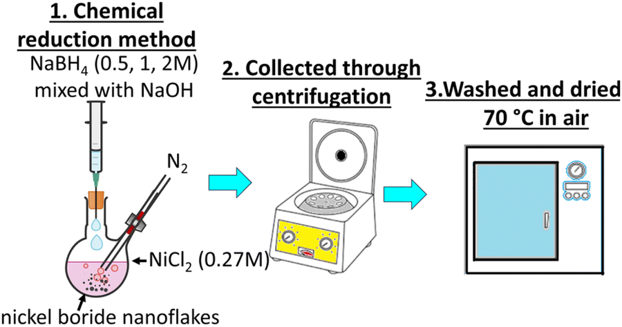 | ||
| Fig. 1 Synthesis route of the 2D nickel boride/borate amorphous/amorphous heterostructures. | ||
| Description | Sample name |
|---|---|
| NaBH4 (0.5 M) + NiCl2 (0.27 M) | NiB/NiBO3-I |
| NaBH4 (1 M) + NiCl2 (0.27 M) | NiB/NiBO3-II |
| NaBH4 (2 M) + NiCl2 (0.27 M) | NiB/NiBO3-III |
2.2 Characterization techniques
Phase analysis of the as-prepared heterostructures was conducted by Powder X-ray diffraction (XRD) using a Siemens D500 (40 kV, 30 mA) diffractometer from Germany with Cu-Kα radiation (8.04 keV). The specimens were scanned in a 2θ range between 10° and 80° with a 0.03° step size, at 2 s per step and rotated at a speed of 30 rpm. Phase analysis of the 2D nanoparticles after electrocatalysis could not be performed as 0.005 mg was used for all electrochemical measurements which is below the instrument's detection limit.A FEI Tecnai 20 (Transmission Electron Microscope) was used for morphological observations of all samples. In addition, a FEI Titan 80–300 kV FEG S/TEM (Scanning/Transmission Electron Microscope) equipped with an Element energy dispersive X-ray spectroscopy (EDX) detector was used for high resolution imaging, electron diffraction and elemental mapping of the NiB/NiBO3-II sample. Prior to their imaging, the nanoparticles were drop casted directly onto a carbon coated Cu TEM grid, after being mixed with ethanol and ultrasonicated for 20 minutes.
Their specific surface area and porosity was determined by nitrogen (N2) adsorption/desorption measurements performed at 77 K using a Nova 2400e Surface Area Analyzer (Quantachrome, UK). The specific surface area of the samples was calculated from the N2 adsorption data at relative pressures between 0.05 and 0.30, by employing the Brunauer–Emmett–Teller (BET) multi-point method.31 The pore size distributions and volumes in the macro- (>50 nm) and meso-range (2–50 nm) were calculated using the Barrett–Joyner–Halenda (BJH) method from the desorption branch of the isotherm.32 All samples were outgassed at 150 °C under vacuum for 4 h prior to their N2 adsorption/desorption analysis.
A Kratos AXIS Ultra DLD X-ray photoelectron spectrometer (XPS) in ultra-high vacuum using an Al-Kα X-ray source (1486.7 eV) was used for the chemical analysis of the as-prepared samples. The Casa XPS software was used for data analysis, and calibrated using the surface adventitious C 1s peak at 284.5 eV. XPS characterization of the samples could not be performed after electrocatalysis due to the small mass of the catalyst which is under the instrument's detection limit.
The magnetic measurements were performed using the ACMS option of the Physical Properties Measuring System (PPMS, Quantum designed). The real and imaginary parts of the magnetic ac-susceptibility were measured with an ac-magnetic field amplitude of 5 Oe and frequencies f = 111 Hz, 1111 Hz, 5111 Hz, and 10 kHz.
Prior to AFM, Conductive-Atomic Force Microscopy and all electrochemical measurements, an ink containing the heterostructures was prepared by dispersing 5 mg of the powder sample in 5% Nafion (20 μL, Sigma-Aldrich), with 490 μL of ethanol and 490 μL of ultrapure water, then ultrasonicated for 20 min.
Samples for AFM investigations were prepared by drop casting 10 μL of the prepared ink onto 18 mm × 18 mm ITO-coated glass substrates (SPI Supplies, 06465-AB). After allowing the samples to dry, height images were obtained using AFM (Asylum Research, MFP-3D) with a Si probe (Nanosensors, NCH) with a nominal resonance frequency of 330 kHz, a tip radius less than 8 nm, and a spring constant of 42 N m−1. Roughness values were averaged from three 5 μm images. Conductive atomic force microscopy (C-AFM) investigations were carried out using the same AFM equipped with a C-AFM cantilever holder (Asylum Research, ORCA with 2 nA/V sensitivity) and a conductive probe (Nanosensors, PPP-EFM) with a nominal resonance frequency, tip radius, and spring constant of 75 kHz, 7 nm, and 2.8 N m−1, respectively. The current–voltage (IV) spectroscopic measurements were conducted in contact mode in a voltage range of +5.0 to −5.0 V with a 1 Hz, 2 cycle triangle waveform initially ramping up from 0 V and applied from the ORCA holder to the sample through the ITO electrode, with the current being measured in the ORCA holder. Before IV measurements, the current was zeroed by applying a small offset. The force applied to the surface during IV measurements was 532 ± 43 nN. Assuming the mechanical properties of each sample are similar, and that tip wear is minimal, the applied force will result in similar contact areas. The reported sample resistances were determined as the inverse slope of the current in a linear range during the application of positive bias (typically 2 to 4.5 V), under the assumption that other resistances were zero. 20 IV sweeps were measured on each sample within a 100 nm × 100 nm area, utilizing a grid-based approach. C-AFM cannot account for changes in sample thickness. The samples were measured sequentially with the same probe. Subsequently, the first sample was measured again and was found to have retained 90% of its original resistance. This consistency indicates that the potential risk of contamination or tip wear does not significantly affect the measurement of current.
A three-electrode cell connected to an Autolab potentiostat (PGSTAT204 with a FRA32M Module, Metrohm) interfaced to a PC with Nova 2.0 software was used for performing the electrochemical measurements. Plain distilled water (pH 7) was used as the electrolyte. A rotating disk glassy carbon (GC) electrode (3 mm diameter, Metrohm) was used as the working electrode instead of a conventional stationary electrode, such as a carbon cloth, to minimise oxygen and hydrogen bubble formation on the electrode's surface during water electrolysis, as well as to enhance mass transfer rates and gas diffusion. A silver/silver chloride (AgCl, 3 M KCl, Metrohm) electrode was used as the reference electrode, and a graphite rod as the counter electrode (MW-4131, BASi). The only disadvantage of using a rotating disc GC electrode as the working electrode is that electrode characterization after water electrolysis measurements cannot be performed due to the small mass of electrocatalyst used, which is far below the detection limit of XPS and of XRD, as already stated. To maintain the pH of the electrolyte at pH7 throughout the electrochemical experiments a borate buffer solution (pH 7) was prepared by mixing 50 mL of (0.2 M KH2PO4, >99% Sigma-Aldrich) and 29.63 mL of sodium hydroxide (0.2 M NaOH, ≥97% Sigma-Aldrich) in 120 mL of distilled water. The borate buffer solution does not participate in the water electrolysis reactions. Prior to all electrochemical measurements, using the drop-casting technique, 10 μL of the ink containing 5 mg of powder sample, was drop-casted onto the polished glassy carbon electrode with a 0.07 cm2 surface area. The film formed had a loading amount of 0.21 mg cm−2 powder sample. The glassy carbon electrode was polished before drop-casting using a polishing cloth and aluminium oxide powder (grain size 0.3 μm). During the electrochemical measurements, the working electrode was rotated at 2000 rpm by a rotation unit (Metrohm) to eliminate bubbles. All measured potentials were converted to the reversible hydrogen electrode (RHE), according to the equation ERHE = EAg/AgCl + 0.1976 + 0.0591 pH. Linear sweep voltammogram measurements for all samples were performed once and not in triplets.
Electrochemical impedance spectroscopy (EIS) was performed at the open circuit potential (OCP) using an AC perturbation of 10 mV in the frequency range from 100 kHz to 1 Hz. The uncompensated resistance Rs was determined from the Nyquist plot (Fig. S1†) and applied for ohmic drop correction following the equation Ec = Ee − iRs, where Ec is the corrected potential and Ee is the experimental potential (Table S1†).33 The raw data with no iRs correction is presented in the ESI Section.† The HER and OER activity were evaluated by linear sweep voltammetry (LSV) at a scan rate of 5 mV s−1 under a N2 gas (>99.999%, BOC) atmosphere. The stability performance of the powder samples was studied by performing 100 scans at a scan rate of 5 mV s−1.
The ECSA for each sample was determined by measuring the electrochemical double layer capacitance (Cdl) from the scan rate CV dependent plot. CV measurements in the non-faradaic region (around the 0.62 V versus RHE), with scan rates of 20, 40, 60, 80, 100 and 120 mV s−1. The Cdl values were obtained by measuring gradients of current density versus scan rate for each sample. The slope of linear fit was calculated as the Cdl. A specific capacitance was of 20 μF cm−2 was used here for a flat surface at pH 7. The ECSA was calculated according to the equation ECSA = Cdl/20 μF cm−2 cmECSA2.
3 Results and discussion
3.1 Phase observations
The three X-ray diffraction patterns of the three samples are presented in Fig. 2, where their amorphous crystalline structure is confirmed as no distinctive diffraction peaks are present in any of the three patterns. As reported in the literature, the structure of metal borides when prepared by a chemical reduction method using NaBH4 as the reducing agent in protic solvents is amorphous, and can become crystalline when heated to 250 °C and higher.26 In detail, NiB/NiBO3-I exhibited no diffraction peaks between 20° and 80°, NiB/NiBO3-II and NiB/NiBO3-III showed a broad diffraction peaks between 30° and 40°, centred at ∼35° which may be attributed to the amorphous state of Ni–B–O phase (COD ID 96-901-1452) corresponding to the (121) crystallographic plane with d = 2.6468 Å.21 NiB/NiBO3-II exhibited an additional broad diffraction peak between 40° and 50°, centred at ∼45°, most possibly assigned to the Ni–B amorphous phase (COD ID 96-900-8948) for the (111) crystallographic plane with d = 2.0047 Å.34 A suggested reduction reaction mechanism for the formation of NiB phase is outlined in reaction (1), whereas the formation of NiBO3 phase is described in reaction (2). Sodium chloride (NaCl) and boric acid (B(OH)3) are both water soluble and can be removed while washing the powder precipitates with water.| NiCl2 + 2NaBH4 + 3H2O → NiB + 2NaCl + 5.5H2 + B(OH)3 | (1) |
| NiB + ⅔O2 → NiBO3 | (2) |
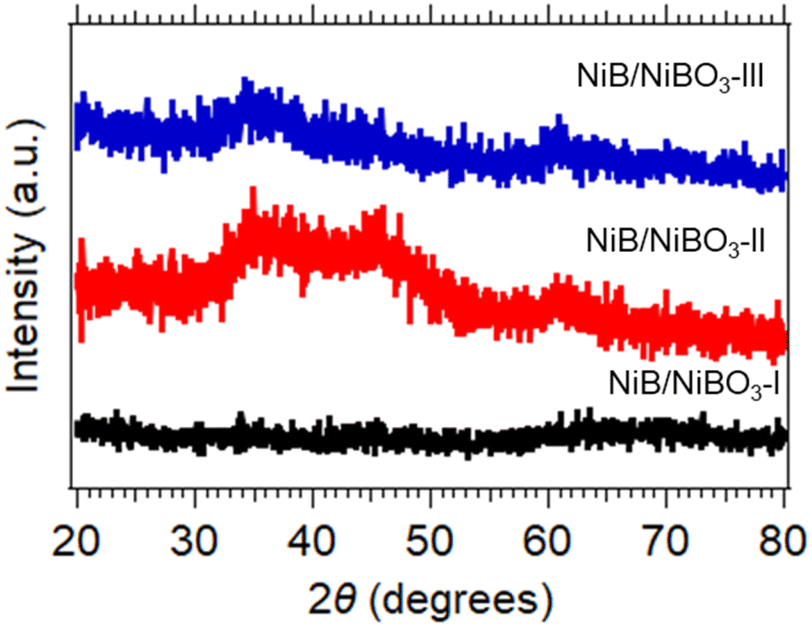 | ||
| Fig. 2 XRD patterns of NiB/NiBO3-I, NiB/NiBO3-II and NiB/NiBO3-III. | ||
3.2 Morphological observations, specific surface area and pore size distribution
All three TEM images of the as-prepared samples are presented in Fig. 3 and S2.† Their sheet-like morphology is evident with almost transparent features, indicating the ultrathin thickness of the nanosheets. No crystal fringes were present in the high-resolution TEM images (Fig. S2†) of NiB/NiBO3 samples, confirming their amorphous crystal structure. Meanwhile, in the same figure (Fig. S2,† indicative areas enclosed with red dashed lines), it is noticeable that around the edges of the nanosheets there is a shade difference, which may possibly be the interface between the NiB and NiBO3 phase of the 2D heterostructure. For a more detailed understanding the morphological structure of the heterostructures, sample NiB/NiBO3-II was selected for further analysis. Fig. 4b shows the HAADF image of NiB/NiBO3-II together with the associated area (orange square) selected for EDX elemental mapping (Fig. 4e–h) and the resultant EDX spectrum (Fig. 4i). As can be seen from the elemental mapping, Ni (Fig. 4e) and B (Fig. 4g) are evenly distributed across the samples, whereas O is mainly localised at the edges of the 2D structures (Fig. 4f), especially noticeable in Fig. 4h where the overlay elemental mapping of these three elements is shown. The HRTEM image in Fig. 4c shows clearly that no crystal fringes are present in the sample, whereas the SAED patterns in Fig. 4d confirms its amorphous structure since no diffraction rings are observed.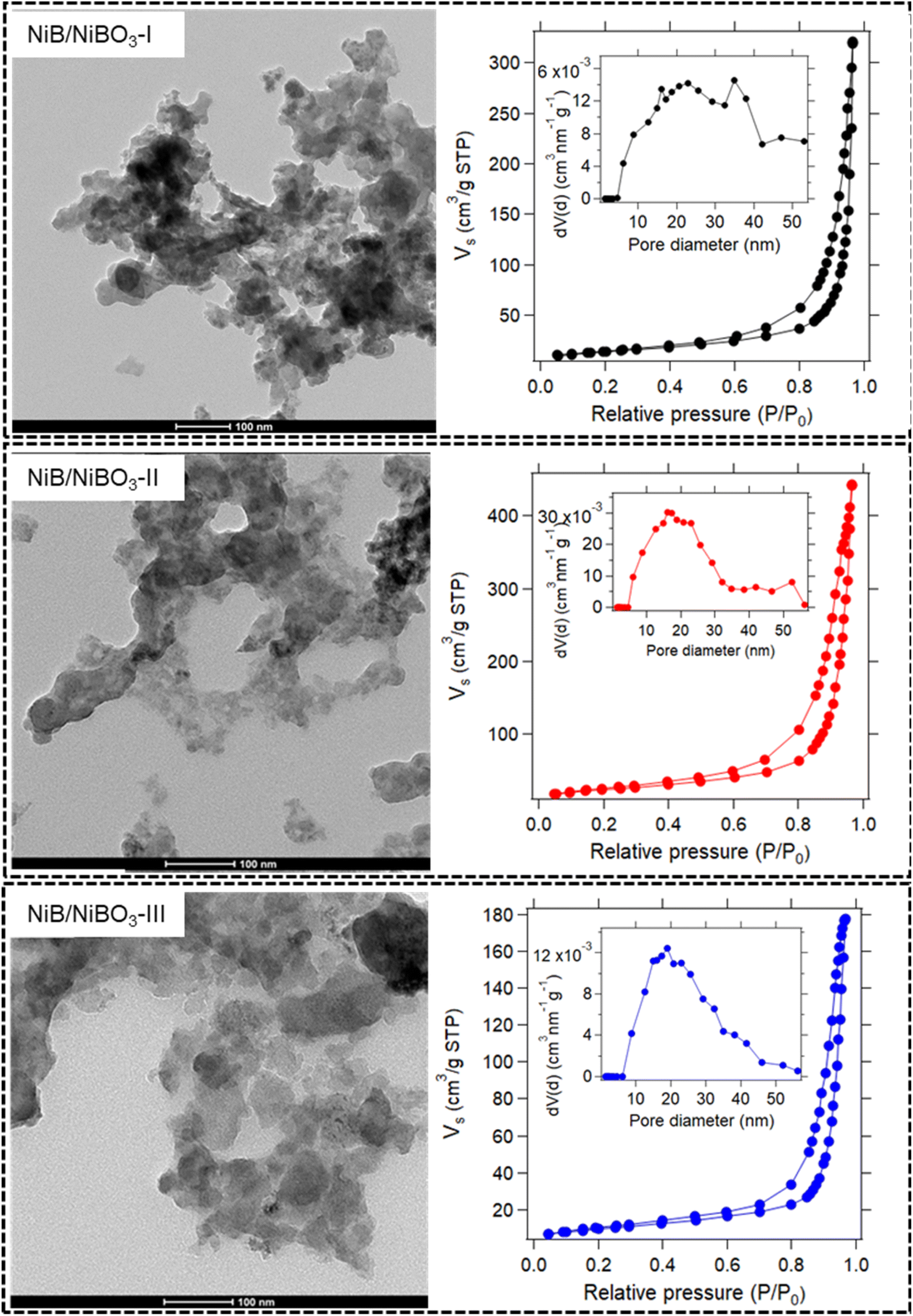 | ||
| Fig. 3 TEM micrographs of NiB/NiBO3-I, NiB/NiBO3-II, NiB/NiBO3-III including their nitrogen adsorption–desorption isotherms and their corresponding pore size distribution curve (inset). | ||
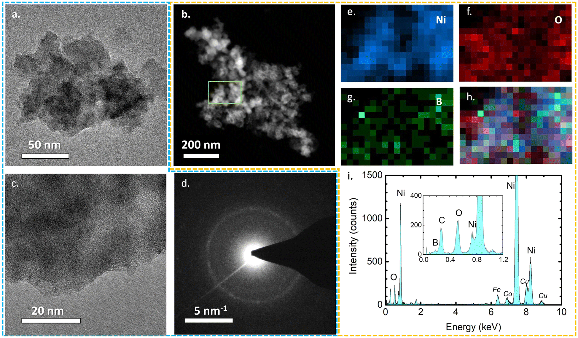 | ||
| Fig. 4 TEM image (a), high angle annular dark filed (HAADF) image (b), HRTEM image (c), SAED pattern (d) energy dispersive X-ray spectroscopy (EDAX-EDX) elemental mapping of Ni (e), O (f), B (g), overlay of O/Ni/B (h), and EDX spectrum (i), of NiB/NiBO3-II. | ||
N2 adsorption/desorption isotherms of all three samples are shown in Fig. 3, together with their pore size distribution curves. All three isotherms belong to a type IV with a H3 type hysteresis loop, associated with large mesopores and macropores.35,36 The lack of knee features at low relative pressures in all three isotherms, indicates an extremely weak adsorbate–adsorbent interaction, representative of samples with no micropores. The understanding is that the individual particles are themselves non-porous. Rather, it is the inter-particulate spaces between the particles, which generates the pore volume and gives rise to hysteresis and the resultant ‘pore size distribution.’ The term ‘pores,’ as used here, is interchangeable with ‘interparticulate void space.’
Across the three samples, the pore size distributions are broadly similar, i.e. pores exist in the range 5–50 nm approximately. The calculated average pore sizes (Table 2) range from 38.6 to 31.9 nm, with the smallest pore size attributed to NiB/NiBO3-III. The pore size decrease is inversely proportional to the concentration of NaBH4 used for the synthesis, which strongly influences the NiBO3 layer formation.
| Sample name | Specific surface area (m2 g−1) | Average pore diameter (nm) | Total pore volume (cm3 g−1) |
|---|---|---|---|
| NiB/NiBO3-I | 51.4 | 38.6 | 0.51 |
| NiB/NiBO3-II | 86.7 | 32.3 | 0.72 |
| NiB/NiBO3-III | 34.5 | 31.9 | 0.29 |
The surface areas of the samples vary quite significantly (see Table 2), with values proportional to the measured pore volumes. Since the pore sizes of these samples are relatively similar, the pore volume (or interparticulate pore space) of the samples is considered the most significant factor influencing the surface area. It is worth noting that the measured pore volume of NiB/NiBO3-III is less than half that of NiB/NiBO3-II.
An explanation for this substantial decrease in pore volume is the doubling of the concentration of NaBH4 used for NiB/NiBO3-III relative to NiB/NiBO3-II. During synthesis, higher concentrations of NaBH4 will mean more nickel ions being reduced to nickel boride and further oxidised to nickel borate. These nickel borate layers will act to partially fill what would otherwise be interparticulate void space. As such, NiB/NiBO3-III is expected to have a dense 2D heterostructure, relative to NiB/NiBO3-I and NiB/NiBO3-II.
There appears to be a threshold concentration of NaBH4 of approximately 1 M, beyond which far greater reduction of nickel ions to nickel boride and nickel borate occurs, resulting in additional layer formation and lower pore volume/surface area. Optimal nanosheet morphology was achieved by using 1 M of NaBH4 and 0.27 M of NiCl2. By forming an optimal layer of nickel borate on the fringes of the 2D structures, these structures are less tightly grouped, thus yielding a low bulk density 2D heterostructure with high surface area and high pore volume.
3.3 XPS analysis
The chemical state and surface composition of the three samples were evaluated by XPS, with the high-resolution spectra of Ni 2p, B 1s, and O 1s being displayed in Fig. 5. In detail, the Ni 2p spectra of the three NiB/NiBO3 samples (Fig. 5a, d and g) is consisted of two main peaks located at ∼856 eV and ∼873.6 eV, and two satellite peaks located at ∼861.7 and ∼880 eV. The two main Ni peaks were further deconvoluted to four peaks in total. The peaks centred at ∼855.7 eV, ∼873.3 eV correspond to nickel bonded to boron (Ni–B) or metallic Ni (Ni0),37,38 whereas the other two peaks at ∼857 eV and ∼875 eV are related to nickel oxo species such as NiBO3 or NiO.27 Meanwhile, the B 1s spectra of the NiB/NiBO3-I sample (Fig. 5b) exhibits two peaks, with the first located at ∼192 eV assigned to boron nickel interactions (B–N),21,34,39 and the second at ∼198.9 eV related to boron oxo species.9,10,40 On the other hand, for the NiB/NiBO3-II and NiB/NiBO3-III samples, the second boron peak of their B 1s spectra (Fig. 5e and h) was further deconvoluted to two more peaks, centred at ∼198.2 eV and ∼199.8 eV, indicating that the extra available boron during synthesis was further oxidised to B2O3.29 The O 1s spectra is presented in Fig. 5c, f, and i for all three samples. Only one peak is present at ∼532 eV, further deconvoluted to three more peaks at 531.1, 532, and 532.7 eV corresponding to Ni–BO, B–O, and adsorbed oxygen species.41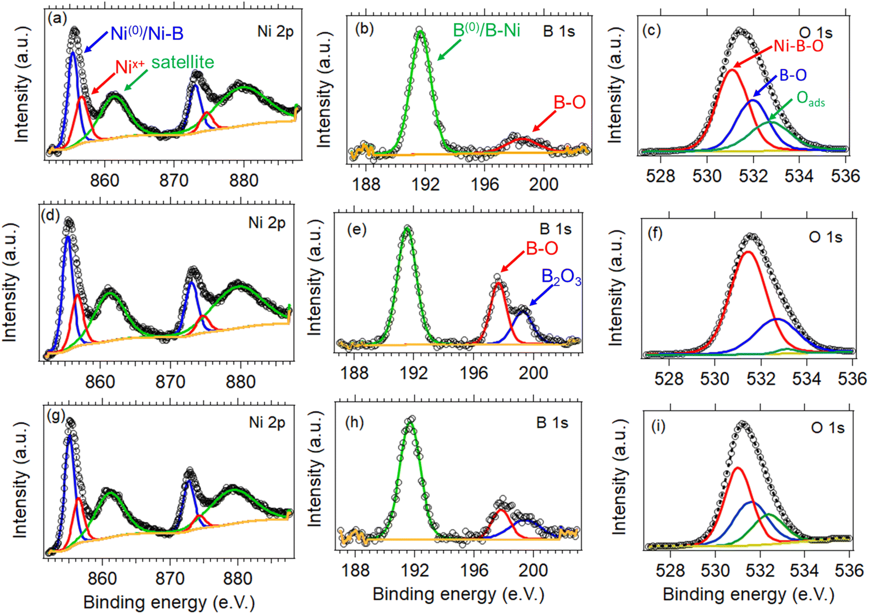 | ||
| Fig. 5 High-resolution XPS spectra of Ni 2p, B 1s and O 1s of the NiB/NiBO3-I (a–c), NiB/NiBO3-II (d–f), and NiB/NiBO3-III (g–i). | ||
The atomic ratio of Ni to B for all three samples together with their allocated atomic percentage of Ni and B, was calculated from their XPS survey spectra, without considering the oxygen contribution, and is presented in Table 3. As expected the Ni:B ratio increases as the concentration of NaBH4 increases during synthesis, with more nickel ions being reduced.42
| Sample name | Ni (at%) | B (at%) | Ni/B atomic ratio |
|---|---|---|---|
| NiB/NiBO3-I | 48.35 | 51.65 | 0.93 |
| NiB/NiBO3-II | 50.74 | 49.26 | 1.03 |
| NiB/NiBO3-III | 64.39 | 35.64 | 1.80 |
3.4 Magnetic performance
The temperature variation of the magnetic ac-susceptibility of all three samples measured under an amplitude of the ac-magnetic field 5 Oe and frequencies f = 111 Hz, 1111 Hz, 5111 Hz, and 10 kHz, in semi-log plots are shown in Fig. 6. The curves representing the real and imaginary parts of the ac-susceptibility display two peaks. The peak at low temperatures, is assigned as peak A, and at higher temperatures, is assigned as peak B. Both peaks appear slightly frequency-dependent. From the peak values of the imaginary magnetic ac-susceptibility, the relaxation time was calculated using the condition 2πfτ = 1, where f is the frequency and τ the relaxation time. The relaxation times versus temperature are reproduced by the Vogel–Fulcher empirical equation43 as seen below:| τ = τ0exp[E/kB(T − T0)] | (3) |
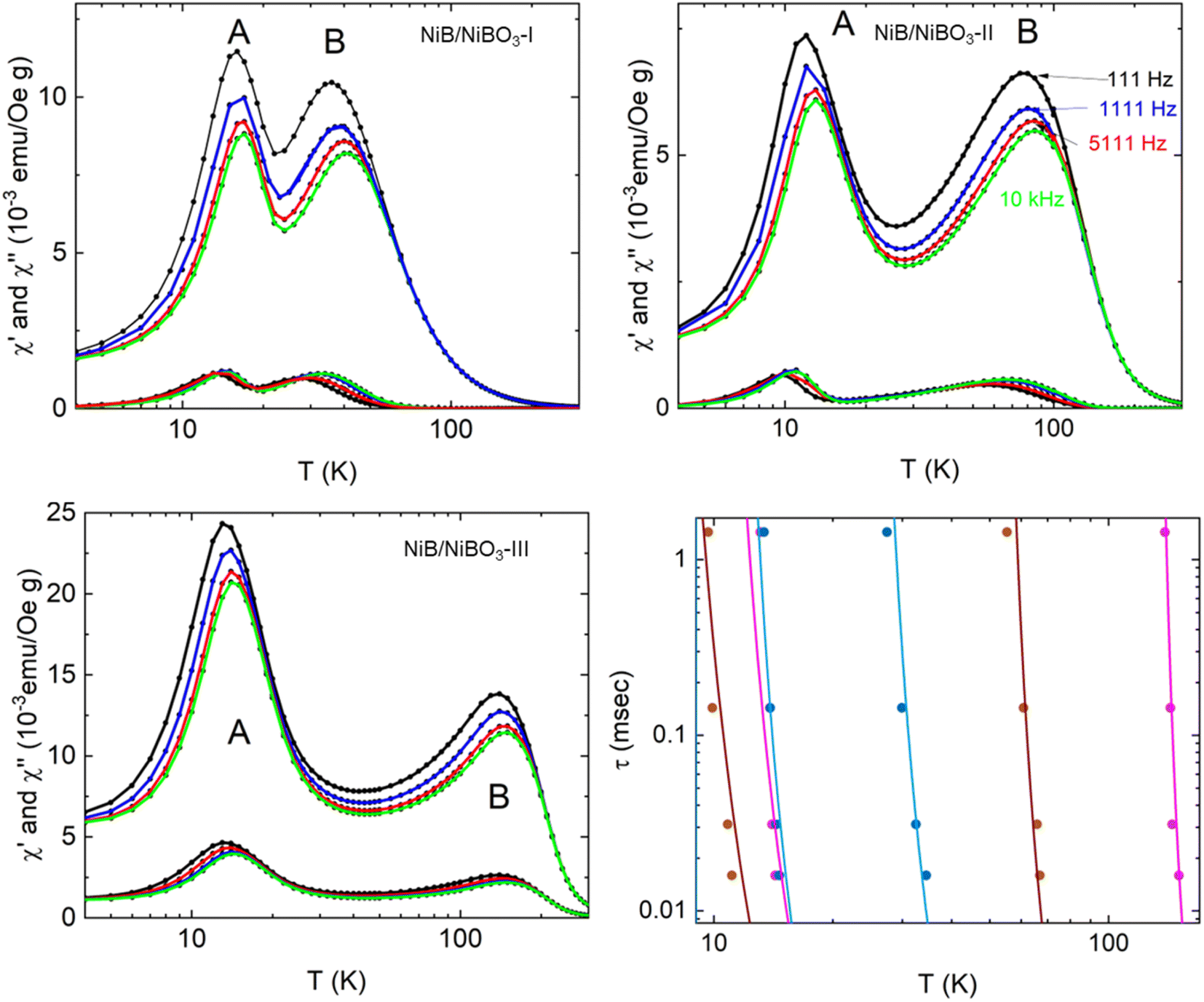 | ||
| Fig. 6 Temperature variation of the real and imaginary fundamental magnetic ac-susceptibility for NiB/NiBO3-I, NiB/NiBO3-II, and NiB/NiBO3-III samples. The data are collected with an amplitude of the ac-magnetic field 5 Oe and frequencies f = 111 Hz, 1111 Hz, 5111 Hz, and 10 kHz. Temperature variation of the relaxation times for the two peaks observed in the three samples. The Vogel–Fulcher empirical equation reproduces the solid lines using the parameters listed in Table 4. | ||
| Sample | Peak A | Peak B | ||||
|---|---|---|---|---|---|---|
| τ 0 (sec) | E (K) | T 0 (K) | τ 0 (sec) | E (K) | T 0 (K) | |
| NiB/NiBO3-I | 5 × 10⁻⁹ | 50 | 9 | 5 × 10⁻⁹ | 110 | 20 |
| NiB/NiBO3-II | 5 × 10⁻⁹ | 55 | 5.1 | 5 × 10⁻⁹ | 169 | 45 |
| NiB/NiBO3-III | 5 × 10⁻⁹ | 59 | 7.5 | 5 × 10⁻⁹ | 250 | 120 |
3.5 AFM analysis
The topography of each sample in the regions of dispersed particles is shown in Fig. 7, with roughness values of 108.5 ± 6.7, 104 ± 18.1, and 125.7 ± 11.5 nm for samples NiB/NiBO3-I, NiB/NiBO3-II, and NiB/NiBO3-III, respectively (Table 5). These roughness values are very similar across the three samples, as expected, since the morphology of each heterostructure is also very similar. This means that topography parameters of these samples are not expected to be responsible for any differences in the electrocatalytic performance of the samples in water splitting. Fig. S3† (Table 5) shows the resistance of each sample, with resistance values decreasing while the concentration of Ni across the samples increases, with mean values of 8658 ± 442, 3109 ± 1674, and 257 ± 36 MΩ for samples NiB/NiBO3-I, NiB/NiBO3-II and NiB/NiBO3-III, respectively. Correspondingly, the measured maximum current increases as the concentration of nickel within the sample also increases, with values of 0.5, 1.1 and 12.8 nA for samples NiB/NiBO3-I, NiB/NiBO3-II and NiB/NiBO3-III respectively. A similar trend is evident in the EIS data obtained (Table S1†), with the charge transfer resistance decreasing while the concentration of Ni increased among the samples. This Indicates that by tuning the nickel concentration in the nickel boride/borate heterostructure, the intrinsic resistivity, electron flow and the rate of reaction on the surface of the heterostructures can be finely tuned. It is worth mentioning that as the atomic concentration of Ni compared to B increases from 48.35 at% in sample NiB/NiBO3-I to 64.39 at% in sample NiB/NiBO3-III, equal to a 1.33 times increase, the resistance values (as assessed from IV slope) in sample NiB/NiBO3-III decreases by ∼34 times whereas the conductivity (as assessed from Imax) increases by ∼26 times, showing an exponential relation of Ni content to intrinsic resistivity and conductivity.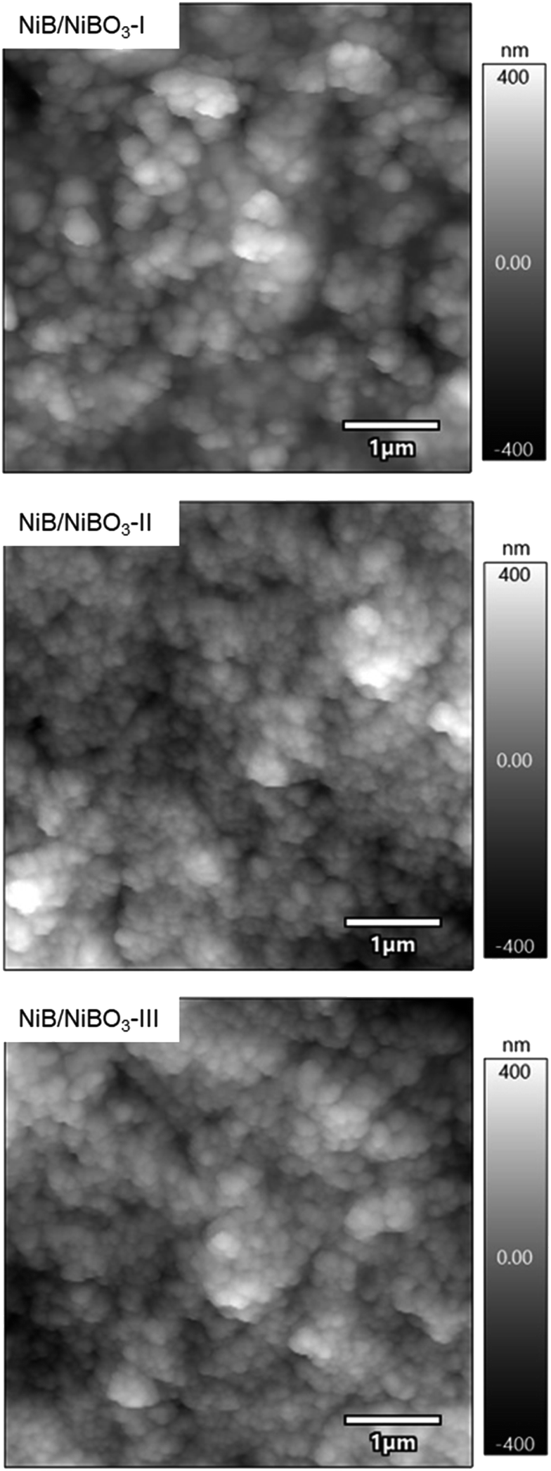 | ||
| Fig. 7 1 μm × 1 μm amplitude modulation mode topography images for samples NiB/NiBO3-I, NiB/NiBO3-II and NiB/NiBO3-III. | ||
| Sample | Roughness (nm) | Resistance (MΩ) | Max current (nA) |
|---|---|---|---|
| NiB/NiBO3-I | 108.5 ± 6.7 | 8658 ± 442 | 0.5 ± 0.06 |
| NiB/NiBO3-II | 104 ± 18.1 | 3109 ± 1674 | 1.1 ± 0.5 |
| NiB/NiBO3-III | 125.7 ± 11.5 | 257 ± 36 | 12.8 ± 1.7 |
3.6 Electrocatalytic properties
The electrocatalytic properties of the three samples were evaluated using a three-electrode cell with buffered distilled water at pH 7 as the electrolyte. Specifically, a borate buffer was used to maintain the pH of the electrolyte at 7 throughout the electrochemical measurements as to properly evaluate the hydrogen and oxygen evolution reactions.46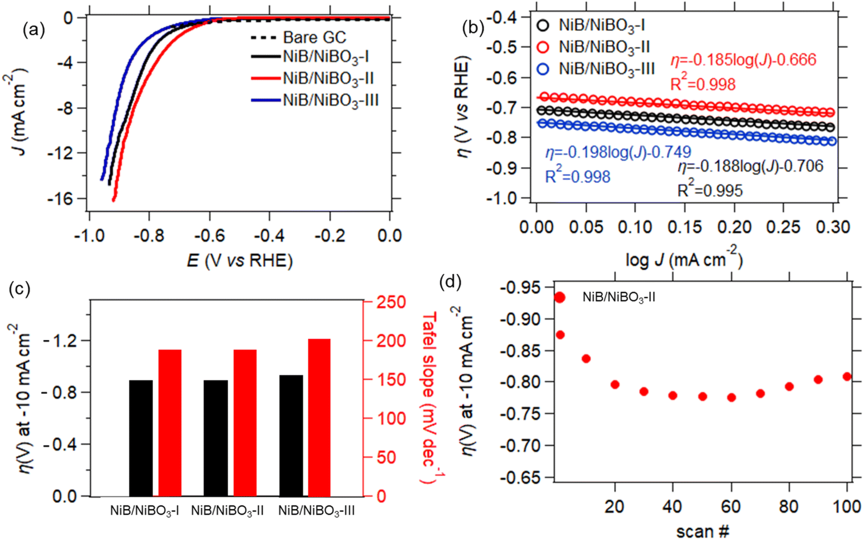 | ||
| Fig. 8 HER LSV curves of NiB/NiBO3-I, NiB/NiBO3-II, NiB/NiBO3-III (a), Tafel plots of the electrodes for HER (b), overpotentials at 10 mA cm−2versus RHE (left) and Tafel slopes (right) for the corresponding heterostructures (c), stability of NiB/NiBO3-II for 100 scans (cycles) (d). | ||
The hydrogen evolution reaction in neutral conditions (pH 7) can be described as a two-step reduction process with both the H2O molecules and the hydronium cation H3O+ participating in the process.50 In the first step, the hydronium cation H3O+ dominate at low cathodic overpotentials close to the equilibrium potential (i.e., 0 V vs. reversible hydrogen electrode (RHE)) as seen in reaction (4). Meanwhile, at high cathodic potentials, the H3O+ cations convert to H2O molecules, with reaction (5) taking place.
| H* + H3O+ + e− → H2 + * | (4) |
| H* + H2O + e− → H2 + OH− | (5) |
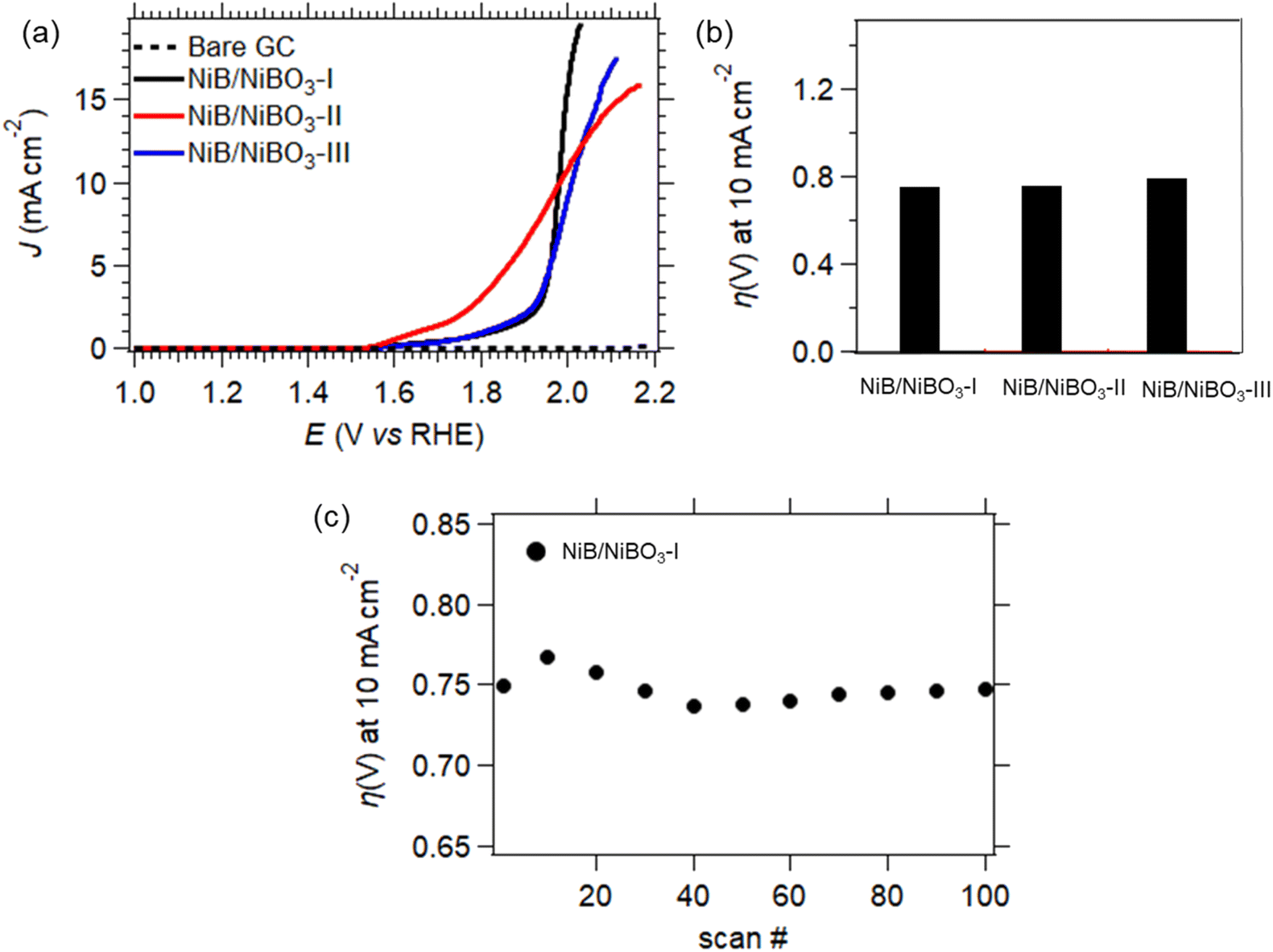
The best performing sample, NiB/NiBO3-II, underwent stability testing by applying 100 consecutive LSV scans, as presented in Fig. 8d. It can be seen that its overpotential value, at current density of −10 mA cm−2, dropped 10% between the 1st and the 20th scan. This drop may be attributed to some partial peeling of the drop casted-ink from the surface of the GC electrode, most probably due to the formation of hydrogen bubbles during HER. This is a very common phenomenon of non-self-supported electrodes.53 Whereas, for the remainder of scans the recorded overpotential values remained stable, showing good overall stability.
 | ||
| Fig. 9 OER LSV curves of NiB/NiBO3-I, NiB/NiBO3-II, NiB/NiBO3-III (a), overpotentials at 10 mA cm−2versus RHE (b), stability of NiB/NiBO3-I for 100 scans (cycles) (c). | ||
A proposed OER reaction mechanisms in neutral conditions (pH 7) is described below:
| 2H2O + * → OH* + H2O + e− + H+ | (6) |
| OH* + H2O → O* + H2O + e− + H+ | (7) |
| O* + H2O → *OOH + e− + H+ | (8) |
| *OOH → O2 + e− + H+ | (9) |
Sample, NiB/NiBO3-I, underwent stability testing by applying 100 consecutive LSV scans, as presented in Fig. 8d. It can be seen that its overpotential values at a current density of 10 mA cm−2 fluctuated between the 1st and 20th scan, with the remainder of overpotential values being stable. This initial fluctuation in overpotential values is perhaps due to the presence of oxygen bubbles on the electrode's surface that formed during OER, and were not successfully removed while rotating the GC electrode at 2000 rpm. It has been reported in the literature that formation of oxygen bubbles during OER is depended to the electrolyte concentration, higher electrolyte concentration induces a smaller bubble diameter.54 Since the OER measurements were performed at pH 7, it is expected a larger formation of oxygen bubbles in comparison to a pH 14 (KOH 1 M) electrolyte, hence being more difficult for the bubbles to detach from the electrode's surface despite its 2000 rpm applied rotation.
4 Conclusions
2D nickel boride/borate amorphous/amorphous heterostructures were successfully synthesised by a simple one pot chemical reduction method. In detail, nickel borides were initially synthesised by using NaBH4 as the reducing agent, while nickel borate was formed on the surface of the as-prepared samples by deliberately exposing them to air while drying overnight. X-ray diffraction revealed that the as-prepared samples were amorphous, whereas TEM images confirmed their 2D structure. XPS analysis established the formation of the nickel borate layer on the surface of the nickel boride samples, forming a 2D heterostructure. This nickel borate layer was observed in the TEM micrographs as a formed thin layer on the fringes of the 2D structures. XPS analysis demonstrated that the atomic concentration of nickel to boron in the heterostructures increased while the concentration of NaBH4 also increased during the synthesis of the nickel borides. This increase in atomic nickel concentration affected the intrinsic resistivity and conductivity of the samples, as revealed by AFM measurements, which directly influenced their electrocatalytic activity, mainly for OER, and magnetic performance. In contrast, HER electrocatalytic activity was the highest for the heterostructure with the highest surface area (86.7 m2 g−1), with an overpotential value of 0.87 V at −10 mA cm−2. Our findings can help provide direction in terms of 2D metal boride/borate amorphous/amorphous heterostructures – specifically, how they can be easily synthesised and tuned to obtain the desired electrocatalytic or magnetic performance for various energy generation or storage applications. The simplicity of our proposed production method of such heterostructures makes it attractive for upscaling to an industrial scale.Author contributions
The manuscript was written through contributions of all authors. All authors have given approval to the final version of the manuscript.Conflicts of interest
There are no conflicts to declare.Acknowledgements
MVS acknowledges the financial support from the UCD Ad Astra fellowship programme, and the Royal Chemical Society for the Research Enablement Grant #72049. QZ and BJR acknowledge the financial support of Science Foundation Ireland (SFI) under the US-Ireland R&D Partnership Programme Grant Number SFI/21/US/3765. HR-TEM and EDX analysis were performed at the SFI-funded CRANN Advanced Microscopy Laboratory (AML).References
- K. S. Novoselov, A. K. Geim, S. V. Morozov, D. Jiang, Y. Zhang, S. V. Dubonos, I. V. Grigorieva and A. A. Firsov, Science, 2004, 306, 666–669 CrossRef CAS PubMed
.
- J. N. Coleman, Adv. Funct. Mater., 2009, 19, 3680–3695 CrossRef CAS
- C. N. R. Rao, A. K. Sood, K. S. Subrahmanyam and A. Govindaraj, Angew. Chem., Int. Ed., 2009, 48, 7752–7777 CrossRef CAS PubMed
- R. C. Selhorst, E. Puodziukynaite, J. A. Dewey, P. Wang, M. D. Barnes, A. Ramasubramaniam and T. Emrick, Chem. Sci., 2016, 7, 4698–4705 RSC
- P. Wang, R. Selhorst, T. Emrick, A. Ramasubramaniam and M. D. Barnes, J. Phys. Chem. C, 2019, 123, 1506–1511 CrossRef CAS
- X. Zhou, X. Hu, J. Yu, S. Liu, Z. Shu, Q. Zhang, H. Li, Y. Ma, H. Xu and T. Zhai, Adv. Funct. Mater., 2018, 28, 1706587 CrossRef
- D. Dev, M. S. Shawkat, A. Krishnaprasad, Y. Jung and T. Roy, IEEE Electron Device Lett., 2020, 41, 1440–1443 CAS
- Y. Liu, Y. Fang, D. Yang, X. Pi and P. Wang, J. Phys.: Condens. Matter, 2022, 34, 183001 CrossRef CAS PubMed
- F. A. Ghafar, D. Etherton, S. Liu, C. Buckley, N. English, D. Silvester-Dean and M. V. Sofianos, J. Electrochem. Soc., 2022, 169, 096507 CrossRef
- B. Fu, V. Tzitzios, Q. Zhang, B. Rodriguez, M. Pissas and M. V. Sofianos, Nanomaterials, 2023, 13, 300 CrossRef CAS PubMed
- L. Teitz and M. Caspary Toroker, Adv. Funct. Mater., 2020, 30, 1808544 CrossRef CAS
- Q. Zhang, S. Zuo, P. Chen and C. Pan, InfoMat, 2021, 3, 987–1007 CrossRef CAS
- Y. Xi, J. Zhuang, W. Hao and Y. Du, ChemElectroChem, 2019, 6, 2841–2851 CrossRef CAS
- L. Maggini and R. R. Ferreira, J. Mater. Chem. C, 2021, 9, 15721–15734 RSC
- H. N. Dhandapani, D. Mahendiran, A. Karmakar, P. Devi, S. Nagappan, R. Madhu, K. Bera, P. Murugan, B. R. Babu and S. Kundu, J. Mater. Chem. A, 2022, 10, 17488–17500 RSC
- S. Anantharaj, J. Kennedy and S. Kundu, ACS Appl. Mater. Interfaces, 2017, 9, 8714–8728 CrossRef CAS PubMed
- P. F. Liu, S. Yang, B. Zhang and H. G. Yang, ACS Appl. Mater. Interfaces, 2016, 8, 34474–34481 CrossRef CAS PubMed
- A. Karmakar, B. B. Kamble, R. Madhu, P. Gudlur and S. Kundu, J. Mater. Chem. A, 2023, 11, 26023–26043 RSC
- R. Madhu, A. Karmakar, K. Karthick, S. Sam Sankar, S. Kumaravel, K. Bera and S. Kundu, Inorg. Chem., 2021, 60, 15818–15829 CrossRef CAS PubMed
- J. H. Han, Y. Y. Hwang, S. Park, J. Shin, K. J. Yoon and Y. J. Lee, J. Mater. Chem. A, 2022, 10, 25055–25062 RSC
- P. Chen, S. Zhang, Y. Fan, W. Yang and X. Luo, Mater. Adv., 2023, 4, 1363–1371 RSC
- N. Yang, H. Cheng, X. Liu, Q. Yun, Y. Chen, B. Li, B. Chen, Z. Zhang, X. Chen, Q. Lu, J. Huang, Y. Huang, Y. Zong, Y. Yang, L. Gu and H. Zhang, Adv. Mater., 2018, 30, 1803234 CrossRef PubMed
- Z. Dong, F. Lin, Y. Yao and L. Jiao, Adv. Energy Mater., 2019, 9, 1902703 CrossRef CAS
- H. Zhao, F. Li, S. Wang and L. Guo, Acc. Mater. Res., 2021, 2, 804–815 CrossRef CAS
- F. Zhao, H. Liu, H. Zhu, X. Jiang, L. Zhu, W. Li and H. Chen, J. Mater. Chem. A, 2021, 9, 10169–10179 RSC
- B. Ganem and J. O. Osby, Chem. Rev., 1986, 86, 763–780 CrossRef CAS
- J. Masa, I. Sinev, H. Mistry, E. Ventosa, M. de la Mata, J. Arbiol, M. Muhler, B. Roldan Cuenya and W. Schuhmann, Adv. Energy Mater., 2017, 7, 1700381 CrossRef
- A. C. Brix, D. M. Morales, M. Braun, D. Jambrec, J. R. C. Junqueira, S. Cychy, S. Seisel, J. Masa, M. Muhler, C. Andronescu and W. Schuhmann, ChemElectroChem, 2021, 8, 2336–2342 CrossRef CAS
- J. Hong, S. Mutalik, M. Miola, D. Gerlach, R. Mehrabi K, M. Ahmadi, B. J. Kooi, G. Portale, P. Rudolf, P. P. Pescarmona and L. Protesescu, Chem. Mater., 2023, 35, 1710–1722 CrossRef CAS
-
Y. B. Pottathara, Y. Grohens, V. Kokol, N. Kalarikkal and S. Thomas, in Nanomaterials Synthesis, ed. Y. Beeran Pottathara, S. Thomas, N. Kalarikkal, Y. Grohens and V. Kokol, Elsevier, 2019, pp. 1–25, DOI:10.1016/B978-0-12-815751-0.00001-8
- S. Brunauer, P. H. Emmett and E. Teller, J. Am. Chem. Soc., 1938, 60, 309–319 CrossRef CAS
- E. P. Barrett, L. G. Joyner and P. P. Halenda, J. Am. Chem. Soc., 1951, 73, 373–380 CrossRef CAS
- S. Ma, R. Farla, K. Bao, A. Tayal, Y. Zhao, Q. Tao, X. Yang, T. Ma, P. Zhu and T. Cui, Nanoscale, 2021, 13, 18570–18577 RSC
- W. Yuan, X. Zhao, W. Hao, J. Li, L. Wang, X. Ma and Y. Guo, ChemElectroChem, 2019, 6, 764–770 CrossRef CAS
- L. Shaohua, B. Jingru, L. Hongpeng, J. Guojun and W. Qing, Oil Shale, 2010, 27, 135 CrossRef
- M. V. Sofianos, D. A. Sheppard, M. R. Rowles, T. D. Humphries, S. Liu and C. E. Buckley, RSC Adv., 2017, 7, 36340–36350 RSC
- F. Yang, P. Han, N. Yao, G. Cheng, S. Chen and W. Luo, Chem. Sci., 2020, 11, 12118–12123 RSC
- J. Legrand, S. Gota, M. J. Guittet and C. Petit, Langmuir, 2002, 18, 4131–4137 CrossRef CAS
- J. Wu, M. Hou, Z. Chen, W. Hao, X. Pan, H. Yang, W. Cen, Y. Liu, H. Huang, P. W. Menezes and Z. Kang, Adv. Mater., 2022, 34, 2202995 CrossRef CAS PubMed
- J. A. Schreifels, P. C. Maybury and W. E. Swartz, J. Catal., 1980, 65, 195–206 CrossRef CAS
- W. J. Jiang, S. Niu, T. Tang, Q. H. Zhang, X. Z. Liu, Y. Zhang, Y. Y. Chen, J. H. Li, L. Gu, L. J. Wan and J. S. Hu, Angew. Chem., 2017, 129, 6672–6677 CrossRef
- A. Corrias, G. Ennas, G. Licheri, G. Marongiu and G. Paschina, Chem. Mater., 1990, 2, 363–366 CrossRef CAS
-
E. Vincent and V. Dupuis, in Frustrated Materials and Ferroic Glasses, ed. T. Lookman and X. Ren, Springer International Publishing, Cham, 2018, pp. 31–56, DOI:10.1007/978-3-319-96914-5_2
- A. Roy, V. Srinivas, S. Ram, J. A. De Toro and U. Mizutani, Phys. Rev. B: Condens. Matter Mater. Phys., 2005, 71, 184443 CrossRef
- V. Tzitzios, G. Basina, M. Gjoka, V. Alexandrakis, V. Georgakilas, D. Niarchos, N. Boukos and D. Petridis, Nanotechnology, 2006, 17, 3750 CrossRef CAS
- T. Shinagawa, M. T.-K. Ng and K. Takanabe, ChemSusChem, 2017, 10, 4155–4162 CrossRef CAS PubMed
- C. C. McCrory, S. Jung, J. C. Peters and T. F. Jaramillo, J. Am. Chem. Soc., 2013, 135, 16977–16987 CrossRef CAS PubMed
- L. Wu, Q. Li, C. H. Wu, H. Zhu, A. Mendoza-Garcia, B. Shen, J. Guo and S. Sun, J. Am. Chem. Soc., 2015, 137, 7071–7074 CrossRef CAS PubMed
- Y. Gorlin and T. F. Jaramillo, J. Am. Chem. Soc., 2010, 132, 13612–13614 CrossRef CAS PubMed
- Y. Guo, T. Park, J. W. Yi, J. Henzie, J. Kim, Z. Wang, B. Jiang, Y. Bando, Y. Sugahara, J. Tang and Y. Yamauchi, Adv. Mater., 2019, 31, 1807134 CrossRef PubMed
- M. R. Gennero de Chialvo and A. C. Chialvo, Phys. Chem. Chem. Phys., 2004, 6, 4009–4017 RSC
- P. M. Quaino, M. R. Gennero de Chialvo and A. C. Chialvo, Phys. Chem. Chem. Phys., 2004, 6, 4450–4455 RSC
- P. Wang and B. Wang, ChemSusChem, 2020, 13, 4795–4811 CrossRef CAS PubMed
- H. Qiu, K. Obata, Z. Yuan, T. Nishimoto, Y. Lee, K. Nagato, I. Kinefuchi, J. Shiomi and K. Takanabe, Langmuir, 2023, 39, 4993–5001 CrossRef CAS PubMed
Footnote |
| † Electronic supplementary information (ESI) available: Additional materials characterizations and electrochemical measurements. See DOI: https://doi.org/10.1039/d4se00095a |
| This journal is © The Royal Society of Chemistry 2024 |