
 Open Access Article
 This Open Access Article is licensed under a
 Creative Commons Attribution 3.0 Unported Licence
A solid-state p–n tandem dye-sensitized solar cell†
Sina
Wrede
 a,
Bin
Cai
a,
Fangwen
Cheng
a,
Malin B.
Johansson
a,
Tomas
Kubart
b,
Carl
Hägglund
c and
Haining
Tian
*a
a,
Bin
Cai
a,
Fangwen
Cheng
a,
Malin B.
Johansson
a,
Tomas
Kubart
b,
Carl
Hägglund
c and
Haining
Tian
*a
aDepartment of Chemistry-Ångström Laboratory, Physical Chemistry, Uppsala University, SE-75120 Uppsala, Sweden. E-mail: haining.tian@kemi.uu.se
bDepartment of Electrical Engineering, Solid-State Electronics, Uppsala University, SE-75120 Uppsala, Sweden
cDepartment of Materials Science and Engineering, Solar Cell Technology, Uppsala University, SE-75120 Uppsala, Sweden
First published on 18th January 2024
Abstract
The development of p–n tandem dye-sensitized solar cells (t-DSCs) offers the potential for substantial open-circuit voltages, holding great promise for a wide range of applications, particularly in the fields of photovoltaics and photoelectrochemical devices. Most reported t-DSCs are liquid-based, and suffer from unsatisfactory stability due to the leakage of liquid electrolytes and photovoltage that is limited to the energy difference of the two utilized semiconductors. In this study, we present the first realization of a solid-state p–n tandem dye-sensitized solar cell that incorporates both p-type and n-type solid-state dye-sensitized solar cells (ssDSCs) by using a transparent indium-doped tin oxide (ITO) back contact for both sides. Notably, this tandem system shows a remarkable open-circuit voltage of 1.4 V, surpassing the constraints of its liquid-based counterparts. Although the performance variations between p-ssDSCs and n-ssDSCs hint at challenges related to charge recombination and the efficiency of p-ssDSCs, this study underscores the significant potential inherent in solid-state tandem configurations.
Introduction
Solar cells, with conversion of abundant and clean solar energy into electricity, have emerged as a prominent technology in the race to reduce our dependence on fossil fuels and combat climate change. Among the various photovoltaic technologies, dye-sensitized solar cells (DSCs) have garnered significant attention due to their cost-effectiveness, ease of fabrication, and tunable optical properties.1–4 With the development of traditional n-type DSCs (n-DSCs) and p-type DSCs (p-DSCs) based on liquid electrolytes, the concept of p–n tandem DSCs has been proposed to improve cell efficiencies and also realized based on sharing a redox couple in liquid electrolytes.5–16However, the liquid p–n tandem DSCs (t-DSCs) have been challenged by leakage of electrolyte and stability issues. Moreover, the theoretical photovoltage (cumulative in a series design) of the liquid p–n tandem DSC is also limited by the energy difference between the conduction band (CB) of n-type semiconductors, such as TiO2, used in n-DSCs and the valence band (VB) of p-type semiconductors, such as NiO, used in p-DSCs, typically ca. 1 V (Fig. 1A).9,10 To overcome these hurdles, we previously proposed the concept and design principle of p–n tandem solid-state dye-sensitized solar cells (t-ssDSCs)17 in which a hole transport material (HTM) and electron transport material (ETM) are used to replace the liquid electrolyte to extract holes and electrons from the dye-sensitized photoanode and dye-sensitized photocathode, respectively. If both photoelectrodes are then connected by a transparent conductor, it has been proposed that the photovoltage (Vssoc) of p–n t-ssDSCs should be able to overcome the photovoltage limit in liquid p–n t-DSCs (Vliquidoc) since the two half cells do not need to share the same redox couple, possibly reaching up to 2 V with suitable materials and device optimization (Fig. 1B).17 However, until now, the concept has not been realized to show that such a device really could surpass the limitations of liquid t-DSCs.
 | ||
| Fig. 1 Potential diagram for a (A) liquid and (B) solid-state p–n tandem DSC. ΔEn: theoretical photovoltage of an n-DSC; ΔEp: theoretical photovoltage of a p-DSC; ECB,TiO2: the conduction band of TiO2; EVB,NiO: the valence band of NiO. | ||
Owing to the development of solid-state n-type DSCs (n-ssDSCs)18–20 and recent good progress on solid-state p-type DSCs (p-ssDSCs),21–26 the time is ripe to combine p- and n-type ssDSCs to realize the first p–n-type solid-state tandem device. Conventional designs of ssDSCs feature a metal back contact, meaning incident light is obstructed from one side of the photoelectrode stack. The incorporation of transparent counter electrodes in ssDSCs offers a dual benefit: it not only facilitates the penetration of incident light, a crucial aspect for various DSC applications like windows27,28 or agrivoltaics,29–31 but it also unlocks the potential for the fabrication of a tandem device. While semi-transparent n-ssDSCs have been demonstrated,32–35 a transparent back contact has not been realized in p-ssDSCs until now. Inspired by the work using indium doped tin oxide (ITO) as a back contact in n-ssDSCs32 and the transparent conductive layer in tandem solar cells,36–39 we herein present the first realization of a p–n t-ssDSC that incorporates both a p-ssDSC and n-ssDSC connected by a transparent ITO conductive layer in a series configuration. The resulting p–n t-ssDSC is semi-transparent and boasts an open-circuit voltage of 1.4 V, surpassing the theoretical voltage limitation of its liquid counterpart sharing one redox couple.
Experimental section
Materials
All chemicals were purchased from Sigma-Aldrich and used directly unless stated otherwise. Fluorine-doped tin-oxide coated glass (FTO, TEC15) was purchased from Pilkington. TiO2 paste (Dyesol, 30NR-T) was purchased from Dyesol. D35 was purchased from Dyenamo. Spiro-OMeTAD (sublimed grade) was purchased from Borun New Material Technology. The NiO screen printing paste10 and PB6 photosensitizer24 were lab-made and available from a previous study.Device fabrication
![[thin space (1/6-em)]](https://www.rsc.org/images/entities/char_2009.gif) :1 v/v) solution overnight. The sensitized films were rinsed with dichloromethane and dried with an N2 flow in order to eliminate physically adsorbed dye molecules on the surface.
:1 v/v) solution overnight. The sensitized films were rinsed with dichloromethane and dried with an N2 flow in order to eliminate physically adsorbed dye molecules on the surface.
Subsequently, atomic layer deposition (ALD) was employed to deposit ZnO on the sensitized electrodes. The films were masked with tape to obtain the desired device structure (see the ESI, Fig. S1†). First, 40 cycles of a stop-flow sequence were used to accommodate the mesoporous nature of the NiO film before 600 cycles of the “normal” sequence were used. The precursors for ALD were diethylzinc (DEZn) and water (H2O) and the temperature in the chamber was 120 °C (stabilization time of 1 h before the start of the deposition process). The stop flow involved a sequence of (1) reduced carrier gas flow, (2) reduced pumping speed through a bypass constriction, (3) precursor injection, (4) precursor exposure, (5) restored pumping speed, and (6) restored carrier gas flow and purging. For the DEZn precursor, the durations of steps 1 to 6 were 2, 2, 0.2, 19.8, 2, and 4 s. During this sequence, the carrier gas flow was reduced from 50 to 10 standard cubic centimeters per minute (sccm) in each of the five unused precursor lines of the system. The TMA line used a flow of 150 sccm during the injection step. In the H2O half-cycle, the duration of steps 1 to 6 was the same, that is, 2, 2, 0.2, 19.8, 2, and 4 s, while the H2O carrier gas flow was increased to 200 sccm and the other precursor line flows were reduced to 10 sccm.
To obtain an extra layer of ZnO, a Zn(acac)2 solution (0.33 M in methanol, filtered using a 0.45 μm syringe filter) was spin-coated onto the ZnO ALD layer (90 μL, 3 s acceleration to 2000 rpm, then 200 s at 2000 rpm). Three layers were deposited and after each layer, the electrode was put on the hotplate for 5 min at 200 °C. After the final layer, the film was put on the hotplate for an additional 15 min at 200 °C. An illustration of the device layout can be found in the ESI, Fig. S1.†
:3 ethanol to Dyesol, 30NR-T w/w) was used. Before deposition via spin-coating (150 μL, 10 s acceleration to 3000 rpm, then 30 s at 3000 rpm), the films were ozone treated for 10 min. The spin coating procedure was repeated the desired times and after each layer, the films were allowed to dry on a hotplate at 115 °C for 5 min. Following the sintering process of the TiO2 film on a hotplate at 500 °C for 30 min, the film was allowed to cool to room temperature. Subsequently, it was submerged in a 0.02 M aqueous TiCl4 solution at 70 °C for 30 min. After rinsing with deionized water, the film was annealed on a hotplate at 500 °C in an ambient atmosphere for 30 min. Once it cooled down to 60 °C, the film was placed in a 0.2 mM D35 in tert-butanol/acetonitrile (1:1 v/v) solution overnight for sensitization.
After rinsing the sensitized electrodes with ethanol and allowing them to dry, a chlorobenzene solution containing 150 mM SPIRO-OMeTAD, 200 mM 4-tert-butylpyridine and 20 mM LiTFSI was applied to create the HTM film. This was achieved by allowing 80 μL of the solution to permeate the sensitized electrode for 30 s and then spin-coating for 30 s at 2000 rpm. Following this, the cells were left in the dark in an air environment for 3 days. An illustration of the device structure can be found in the ESI, Fig. S1.†
Preparation of the transparent back contact for p-ssDSCs and n-ssDSCs
For p-ssDSCs and n-ssDSCs, the transparent ITO back contact electrode was deposited on the ZnO and SPIRO of the respective NiO and TiO2 films. The deposition was done via direct-current magnetron sputtering from a ceramic ITO (90/10, purity 99.99%) sputtering target in a deposition system, CS730 (Von Ardenne). The depositions were carried out for 120 s at a power of 640 W, corresponding to 2 W cm−2, in an Ar + O2 atmosphere (1.8% O2) at a total pressure of 0.6 Pa which resulted in an ITO layer with a thickness of 200–250 nm.For better contact with the crocodile clamps used during device characterization, a small spot of silver paste was deposited on the contacts.
Assembly of p–n t-ssDSCs
The p-ssDSC and n-ssDSC were pressed together with clamps with the p-ssDSC on the top, avoiding contact between the FTO layers of the two films (ESI, Fig. S1†).Solar cell characterization
Absorption spectra were recorded with a diode array spectrophotometer (Agilent 8453) with a home-made film holder.The solar cells were evaluated under an irradiation intensity of 100 mW cm−2, utilizing a Wave Labs SINUS-70 solar simulator that included UV and IR range extenders. In the J–V measurements, a black mask with a 0.2 cm2 aperture area was employed and the voltage was screened in 0.01 V increments with a voltage settling time of 0.1 s. IPCE measurements (ESI, Fig. S6†) were carried out using a setup consisting of a xenon lamp (Spectral Products ASB-XE-175), a monochromator (Spectral Products CM110), and a LabJack U6 data acquisition board.
Results and discussion
The fabricated p–n tandem solid-state dye-sensitized solar cell in our study incorporated well-established materials, such as D3533,42–44 and PB622–24 dyes for sensitizing TiO2 and NiO films, respectively (Fig. 2A). The configuration of the p–n t-ssDSCs, energy alignment of each component, and the individual p-ssDSC and n-ssDSC are illustrated in Fig. 2B and 3. On the basis of our previous work on p-ssDSCs,22,23 we used a compact NiO layer on FTO glass to avoid short circuit with the back contact onto which a PB6-sensitized mesoporous NiO layer was deposited, as shown in Fig. 2. As an electron transport material (ETM), ZnO was chosen since previous studies23,45 show the highest photovoltage with ZnO while maintaining a decent photocurrent (see the ESI, Table S1†). With the hopes of achieving a good pore filling, ZnO was deposited via atomic layer deposition (ALD) where we first used a stop-flow sequence to accommodate the mesoporous nature of the NiO film to deposit a thin layer of ZnO (∼6 nm) before we deposited approx. 100 nm ZnO with “normal” ALD. To protect the film from short-circuits caused by the sputtering of the ITO back contact,32 we added an extra layer of spin-coated Zn(acac)2 that was transformed to ZnO upon heat exposure at 200 °C.23 We found that the combination of ZnO from ALD with the extra layers from Zn(acac)2 solution yielded the best performing cells (ESI, Fig. S2†). This is likely due to a combination of a good pore filling from the ALD with the extra protection of the additional ZnO layer during the consequent sputtering process. Aging was also found to be an important part to get good working cells, and storage in the dark in ambient air improved cell performance significantly (ESI, Fig. S2†), corresponding with previous literature.23,45
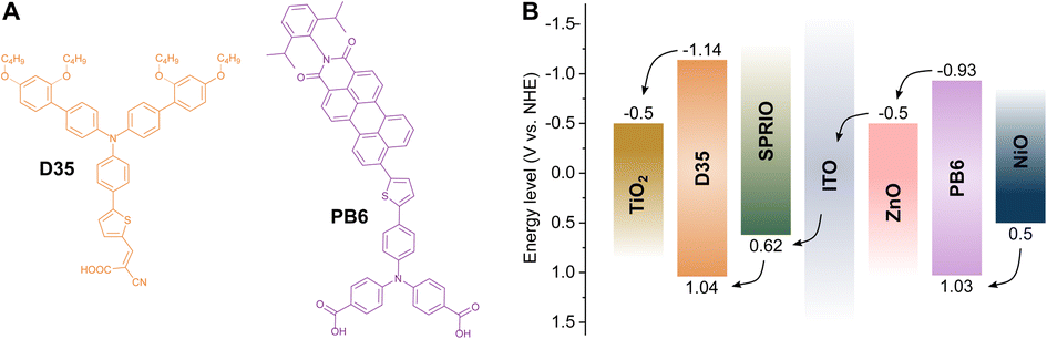 | ||
| Fig. 2 Dye structure (A) and energy level diagram (B) of the components in the p–n t-ssDSC stack. For the energy levels of PB624 and D3544 dyes, the LUMO energy was obtained from the reported ground state oxidation potential (HOMO) and E0−0 transition energy. Spiro-OMeTAD45 energy levels were taken directly from the literature. | ||
 | ||
| Fig. 3 Device structure of p-ssDSC, n-ssDSC and p–n t-ssDSCs. | ||
Inspired by previous work33,41,46 the n-ssDSC was fabricated from a D35-sensitized mesoporous TiO2 layer on a compact TiO2 blocking layer (Fig. 3). D35 was chosen over other dyes due to its favorable absorption wavelength with PB6 in comparison with other commercial dyes and exhibits typically a good photovoltage and current. The hole-transporting material (HTM), a lithium doped Spiro-OMeTAD solution (SPIRO), was spin-coated on the dye-sensitized film.41 The transparent ITO back contact was then directly deposited on the HTM.
To assemble the p–n tandem cell, the p-ssDSC cell was placed on the top due to its lower photocurrent compared to the n-ssDSCs. Even the current published record photocurrent for p-ssDSCs, with a short-circuit photocurrent density (Jsc) of 1 mA cm−2, is still considerably lower than for n-ssDSCs.25 The t-ssDSCs are therefore illuminated from the p-type side since the overall photocurrent is limited by the cell with the lowest current in a series connection, which limits the overall performance in our case (Fig. 3). We additionally adjusted the thickness of the TiO2 in the n-ssDSC to match the photocurrent when shaded by the p-ssDSC on top to suppress unnecessary photo annihilation (ESI, Fig. S3 and S4†). Two layers of the spin-coated meso-TiO2 solution proved to be ideal to match the Jsc of the p-ssDSC of around 0.8 mA cm−2 when shaded by the p-ssDSC on top. This is a critical step in optimizing the performance of the tandem cell to reduce losses and photo annihilation. The resulting solar cells are clearly semi-transparent with a pink color for the p-ssDSC and yellow color for the n-ssDSC (insets in Fig. 4A).
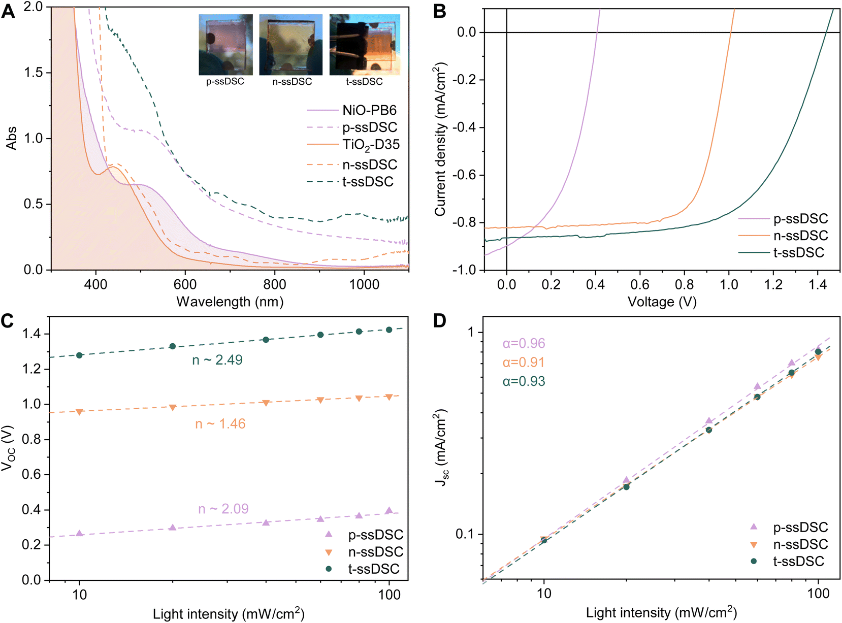 | ||
| Fig. 4 (A) Absorption spectra of dye-sensitized NiO and TiO2 films as well as the fabricated solar cell devices, with pictures of the ss-DSCs as insets. (B) J–V curves of the champion cells. Note that the p-ssDSC is illuminated from the glass side and that the n-ssDSC is shaded by an overlaying p-ssDSC film during measurement. Light intensity dependence of the (C) Voc with the light ideality factor n and (D) Jsc with the power law factor α. | ||
The tandem device showed an orange color but also remained semi-transparent. Absorption spectra were recorded to evaluate the optical properties of all fabricated solar cells. The absorption spectra were obtained for both the dye-sensitized films and the complete solar cells and are shown in Fig. 4A. In the dye-sensitized film, we can clearly see the characteristic and complementary absorption of PB6 and D35 on film and in the final devices, as well as in the IPCE (ESI, Fig. S6†). Upon comparing the absorption spectra of the pure sensitized films to those of the functioning solar cell, we observed that the dyes remained stable during the cell fabrication process. In the absorption spectra of the n-ssDSC, we can clearly see the contributions of the Spiro-OMeTAD HTM which absorbs below 400 nm. Furthermore, it is evident that there is a baseline shift in the absorption spectra for the PB6-based solar cell. This shift can primarily be attributed to the scattering of light by the ZnO/ITO interfacial layer, a phenomenon that could also be visually perceived.
The J–V curves of the champion devices are presented in Fig. 4B, with corresponding photovoltaic performance parameters detailed in Table 1. In the tandem cell, we achieved a power conversion efficiency (PCE) of 0.75%, a Jsc of 0.86 mA cm−2 and an exceptional open-circuit voltage (Voc) of 1.437 V. Notably, the Jsc values of the p- and n-ssDSCs in the tandem configuration align remarkably well, a critical requirement to suppress the unnecessary photo annihilation for tandem devices in series. In this setup, the overall current is governed by the lowest current cell, while the voltages are additive. Our findings clearly demonstrate that the Voc of the tandem device (1.437 V) is the sum of the individual Voc values of the p-ssDSCs (0.407 V) and n-ssDSCs (1.000 V), and is not limited by the difference of the valence band of the photocathode and conduction band of the photoanode like in the liquid-state tandem cell. It is also worth noting an intriguing observation in the tandem device – there is a subtle increase of the current when compared to the n-ssDSC (Fig. 4B). This discrepancy, observed across all fabricated tandem devices, appears to be linked to the scattering effect introduced by the ZnO/ITO layer of the p-ssDSC and the ITO layer of the n-ssDSC. This phenomenon can boost the light absorption by n-ssDSCs and contributes to the amplified current in the tandem configuration.
| Device | PCE (%) | FF (%) | J sc (mA cm−2) | V oc (V) |
|---|---|---|---|---|
| p-ssDSC | 0.166 | 45.6 | 0.89 | 0.407 |
| n-ssDSC | 0.595 | 71.9 | 0.82 | 1.000 |
| t-ssDSC | 0.766 | 62.0 | 0.86 | 1.437 |
To further investigate the fabricated solar cells, light intensity dependencies were recorded. When looking at the dependency of the Voc with light intensity in Fig. 4C, we observe that the p-ssDSC shows a high light ideality factor (n) of 2.09 which is indicative of trap assisted recombination that is typically also reflected in a lower fill factor (FF). The light ideality factor of the n-ssDSC is significantly lower at 1.46. Notably, the p-ssDSCs without the extra spin-coated ZnO layer in addition to ALD showed a higher FF (ESI, Fig. S2†) which indicates that additional transport losses may arise from the extra ZnO layer, despite the higher PCE of the p-ssDSCs with the extra ZnO layer.
Interestingly, the increase of Jsc with light intensity (I), that is generally described by Jsc ∝ Iα, shows a quasi linear behavior for all solar cells (Fig. 4D). A value of α = 1 indicates that all separated free carriers are extracted before recombination, and α < 1 indicates that Jsc depends on bimolecular recombination (i.e., carriers recombine before being extracted).47 Notably, the obtained α = 0.96 from the slope of the log(Jsc) versus log(I) plot for the p-ssDSC is much better than in a previous study with NiO–PB6 cells that only used a ZnO layer from Zn(acac)2.24 This indicates that the ALD ZnO layer achieves a good pore filling and reduces the Langevin recombination between the photo-generated charge carriers, likely due to better charge extraction and transporting abilities.
The spread of J–V parameters of the manufactured devices for p-ssDSC, n-ssDSC and the tandem devices is shown in Fig. 5. It is visible that the p-ssDSCs exhibit higher photovoltaic performance deviation in general and against the sample position (vertically aligned points) compared to the n-type cells. This significant discrepancy, particularly in the Jsc and FF of the p-ssDSC devices, also suggests potential issues related to solar cell fabrication leading to transport losses and recombination.
 | ||
| Fig. 5 J–V parameters of the manufactured p-ssDSCs, n-ssDSC and t-ssDSCs under 1 sun illumination. | ||
Furthermore, the shunt resistance of the p-ssDSC devices is notably lower, measuring 2.7 kΩ cm2, as compared to the n-ssDSCs with a shunt resistance of 15 kΩ cm2. A low shunt resistance is likely caused by the presence of pin-hole contacts within the p-ssDSCs due to the manufacturing, providing an alternative path for photo-generated current. This also contributes to the observed variations in device performance depending on spot selection in the p-ssDSCs.
The series resistances for the p-ssDSC (156 Ω cm2) and n-ssDSC (200 Ω cm2) are similar. As expected, the series resistance of the tandem cell (400 Ω cm2) is close to the sum of the series resistances of the individual devices. However, there is still some additional resistance originating from purely pressing the two cells together in the tandem device.
Despite the challenges and limitations associated with p-ssDSCs in general (see the ESI, Table S1†), and also limited efficiency of the overall device in this study, our results highlight that the open-circuit voltage of a p–n t-ssDSC can surpass the energy difference between the NiO valence band and TiO2 conduction band, approximately 1 V (Fig. 1), which is the theoretical photovoltage limit of p–n liquid t-DSCs sharing one redox couple.17 This achievement confirms the potential of solid-state tandem configurations and their capacity to harness the combined open-circuit voltages of the constituent devices.
Conclusion
In summary, we report the first realization of solid-state p–n tandem dye sensitized solar cells (t-ssDSCs) constructed from a PB6 dye-based p-ssDSC and D35 dye-based n-type DSC with indium tin oxide (ITO) as the back contact. With a good match of dye absorption between PB6 and D35, the solid-state tandem DSC system yielded a short-circuit photocurrent density of up to 0.86 mA cm−2 with a remarkably high open-circuit voltage of up to 1.4 V, which surpasses the theoretical voltage limitations of its liquid counterpart sharing one redox couple. This work represents a significant milestone in the advancement of p–n t-ssDSCs. These innovations hold great promise across a range of applications within the fields of photovoltaics and photoelectrochemical devices, paving the way for sustainable and efficient energy conversion technologies.Conflicts of interest
The authors declare no competing financial interest.Acknowledgements
We would like to gratefully acknowledge the financial support from the Swedish Energy Agency (49278-1), and thank Prof. Gerrit Boschloo for access to his facilities and Dr Fuxiang Ji for his help with spray-coating the TiO2 compact layer. We also acknowledge Myfab Uppsala for providing facilities and experimental support. Myfab is funded by the Swedish Research Council (2019-00207) as national research infrastructure.References
- B. O'Regan and M. Grätzel, A Low-Cost, High-Efficiency Solar Cell Based on Dye-Sensitized Colloidal TiO2 Films, Nature, 1991, 353(6346), 737–740 CrossRef.
- F. T. Kong, S. Y. Dai and K. J. Wang, Review of Recent Progress in Dye-Sensitized Solar Cells, Adv. OptoElectron., 2007, 1–13 CAS.
- A. Hagfeldt, G. Boschloo, L. Sun, L. Kloo and H. Pettersson, Dye-Sensitized Solar Cells, Chem. Rev., 2010, 110(11), 6595–6663 CrossRef CAS PubMed.
- A. B. Muñoz-García, I. Benesperi, G. Boschloo, J. J. Concepcion, J. H. Delcamp, E. A. Gibson, G. J. Meyer, M. Pavone, H. Pettersson, A. Hagfeldt and M. Freitag, Dye-Sensitized Solar Cells Strike Back, Chem. Soc. Rev., 2021, 50(22), 12450–12550 RSC.
- J. He, H. Lindström, A. Hagfeldt and S. E. Lindquist, Dye-Sensitized Nanostructured Tandem Cell-First Demonstrated Cell with a Dye-Sensitized Photocathode, Sol. Energy Mater. Sol. Cells, 2000, 62(3), 265–273 CrossRef CAS.
- A. Nakasa, H. Usami, S. Sumikura, S. Hasegawa, T. Koyama and E. Suzuki, A High Voltage Dye-Sensitized Solar Cell Using a Nanoporous NiO Photocathode, Chem. Lett., 2005, 34(4), 500–501 CrossRef CAS.
- J. Wei, Z. Shao, B. Pan, S. Chen, L. Hu and S. Dai, Toward Current Matching in Tandem Dye-Sensitized Solar Cells, Materials, 2020, 13(13), 2936 CrossRef CAS.
- H. Cheng, M. Ayaz, S. Wrede, G. Boschloo, L. Hammarström and H. Tian, Assessing the Effect of Surface States of Mesoporous NiO Films on Charge Transport and Unveiling an Unexpected Light Response Phenomenon in Tandem Dye-Sensitized Solar Cells, Energy Adv., 2022, 1(5), 303–311 RSC.
- E. A. Gibson, A. L. Smeigh, L. Le Pieux, J. Fortage, G. Boschloo, E. Blart, Y. Pellegrin, F. Odobel, A. Hagfeldt and L. Hammarström, A P-Type NiO-Based Dye-Sensitized Solar Cell with an Open-Circuit Voltage of 0.35 V, Angew. Chem., Int. Ed., 2009, 48(24), 4402–4405 CrossRef CAS.
- A. Nattestad, A. J. Mozer, M. K. R. Fischer, Y. B. Cheng, A. Mishra, P. Bäuerle and U. Bach, Highly Efficient Photocathodes for Dye-Sensitized Tandem Solar Cells, Nat. Mater., 2010, 9(1), 31–35 CrossRef CAS.
- D. Xiong and W. Chen, Recent Progress on Tandem Structured Dye-Sensitized Solar Cells, Front. Optoelectron., 2012, 5(4), 371–389 CrossRef.
- C. J. Wood, G. H. Summers and E. A. Gibson, Increased Photocurrent in a Tandem Dye-Sensitized Solar Cell by Modifications in Push-Pull Dye-Design, Chem. Commun., 2015, 51(18), 3915–3918 RSC.
- P. Ho, S. Thogiti, Y. H. Lee and J. H. Kim, Discrete Photoelectrodes with Dyes Having Different Absorption Wavelengths for Efficient Cobalt-Based Tandem Dye-Sensitised Solar Cells, Sci. Rep., 2017, 7(1), 2272 CrossRef.
- Y. Farré, M. Raissi, A. Fihey, Y. Pellegrin, E. Blart, D. Jacquemin and F. Odobel, A Blue Diketopyrrolopyrrole Sensitizer with High Efficiency in Nickel-Oxide-Based Dye-Sensitized Solar Cells, ChemSusChem, 2017, 10(12), 2618–2625 CrossRef.
- P. Ho, S. Thogiti, L. Q. Bao, R. Cheruku, K. S. Ahn and J. Hong Kim, Enhanced Efficiency via Blocking Layers at Photocathode Interfaces in Cobalt-Mediated Tandem Dye-Sensitized Solar Cells, Sol. Energy, 2018, 161, 9–16 CrossRef CAS.
- O. Langmar, E. Fazio, P. Schol, G. de la Torre, R. D. Costa, T. Torres and D. M. Guldi, Controlling Interfacial Charge Transfer and Fill Factors in CuO-Based Tandem Dye-Sensitized Solar Cells, Angew. Chem., Int. Ed., 2019, 58(12), 4056–4060 CrossRef CAS PubMed.
- H. Tian, Solid-State p-Type Dye-Sensitized Solar Cells: Progress, Potential Applications and Challenges, Sustainable Energy Fuels, 2019, 3(4), 888–898 RSC.
- U. Bach, D. Lupo, P. Comte, J. E. Moser, F. Weissörtel, J. Salbeck, H. Spreitzer and M. Grätzel, Solid-State Dye-Sensitized Mesoporous TiO2 Solar Cells with High Photon-to-Electron Conversion Efficiencies, Nature, 1998, 395(6702), 583–585 CrossRef CAS.
- J. H. Yum, P. Chen, M. Grätzel and M. K. Nazeeruddin, Recent Developments in Solid-State Dye-Sensitized Solar Cells, ChemSusChem, 2008, 1(8–9), 699–707 CrossRef CAS.
- I. Benesperi, H. Michaels and M. Freitag, The Researcher's Guide to Solid-State Dye-Sensitized Solar Cells, J. Mater. Chem. C, 2018, 6(44), 11903–11942 RSC.
- L. Zhang, G. Boschloo, L. Hammarström and H. Tian, Solid State P-Type Dye-Sensitized Solar Cells: Concept, Experiment and Mechanism, Phys. Chem. Chem. Phys., 2016, 18(7), 5080–5085 RSC.
- L. Tian, J. Föhlinger, Z. Zhang, P. B. Pati, J. Lin, T. Kubart, Y. Hua, J. Sun, L. Kloo, G. Boschloo, L. Hammarström and H. Tian, Solid State P-Type Dye Sensitized NiO–Dye–TiO2 Core–Shell Solar Cells, Chem. Commun., 2018, 54(30), 3739–3742 RSC.
- B. Xu, L. Tian, A. S. Etman, J. Sun and H. Tian, Solution-Processed Nanoporous NiO-Dye-ZnO Photocathodes: Toward Efficient and Stable Solid-State p-Type Dye-Sensitized Solar Cells and Dye-Sensitized Photoelectrosynthesis Cells, Nano Energy, 2019, 55, 59–64 CrossRef CAS.
- B. Xu, S. Wrede, A. Curtze, L. Tian, P. B. Pati, L. Kloo, Y. Wu and H. Tian, An Indacenodithieno[3,2-b]Thiophene-Based Organic Dye for Solid-State p-Type Dye-Sensitized Solar Cells, ChemSusChem, 2019, 12(14), 3243–3248 CrossRef CAS.
- H. Cheng, Y. Liu, B. Cai, C. Hägglund, T. Kubart, G. Boschloo and H. Tian, Atomic Layer Deposition of SnO2 as an Electron Transport Material for Solid-State P-Type Dye-Sensitized Solar Cells, ACS Appl. Energy Mater., 2022, 5(10), 12022–12028 CrossRef CAS.
- T. T. T. Pham, S. K. Saha, D. Provost, Y. Farré, M. Raissi, Y. Pellegrin, E. Blart, S. Vedraine, B. Ratier, D. Aldakov, F. Odobel and J. Bouclé, Toward Efficient Solid-State p-Type Dye-Sensitized Solar Cells: The Dye Matters, J. Phys. Chem. C, 2017, 121(1), 129–139 CrossRef CAS.
- J. W. Lee, J. Park and H.-J. Jung, A Feasibility Study on a Building's Window System Based on Dye-Sensitized Solar Cells, Energy and Buildings, 2014, 81, 38–47 CrossRef.
- T. Baron, W. Naim, I. Nikolinakos, B. Andrin, Y. Pellegrin, D. Jacquemin, S. Haacke, F. Sauvage and F. Odobel, Transparent and Colorless Dye-Sensitized Solar Cells Based on Pyrrolopyrrole Cyanine Sensitizers, Angew. Chem., Int. Ed., 2022, 61(35), e202207459 CrossRef CAS PubMed.
- D. A. Chalkias, C. Charalampopoulos, A. K. Andreopoulou, A. Karavioti and E. Stathatos, Spectral Engineering of Semi-Transparent Dye-Sensitized Solar Cells Using New Triphenylamine-Based Dyes and an Iodine-Free Electrolyte for Greenhouse-Oriented Applications, J. Power Sources, 2021, 496, 229842 CrossRef CAS.
- D. Ursu, M. Vajda and M. Miclau, Highly Efficient Dye-sensitized Solar Cells for Wavelength-selective Greenhouse: A Promising Agrivoltaic System, Int. J. Energy Res., 2022, 46(13), 18550–18561 CrossRef CAS.
- J. Barichello, L. Vesce, P. Mariani, E. Leonardi, R. Braglia, A. Di Carlo, A. Canini and A. Reale, Stable Semi-Transparent Dye-Sensitized Solar Modules and Panels for Greenhouse Application, Energies, 2021, 14(19), 6393 CrossRef CAS.
- Y. F. Chiang, C. H. Tsai, P. Chen and T. F. Guo, Bifacial Transparent Solid-State Dye-Sensitized Solar Cell with Sputtered Indium-Tin-Oxide Counter Electrode, Sol. Energy, 2012, 86(6), 1967–1972 CrossRef CAS.
- G. Y. Margulis, M. G. Christoforo, D. Lam, Z. M. Beiley, A. R. Bowring, C. D. Bailie, A. Salleo and M. D. McGehee, Spray Deposition of Silver Nanowire Electrodes for Semitransparent Solid-State Dye-Sensitized Solar Cells, Adv. Energy Mater., 2013, 3(12), 1657–1663 CrossRef CAS.
- K. Aitola, J. Zhang, N. Vlachopoulos, J. Halme, A. Kaskela, A. G. Nasibulin, E. I. Kauppinen, G. Boschloo and A. Hagfeldt, Carbon Nanotube Film Replacing Silver in High-Efficiency Solid-State Dye Solar Cells Employing Polymer Hole Conductor, J. Solid State Electrochem., 2015, 19(10), 3139–3144 CrossRef CAS.
- J. Zhang, J. Feng, Y. Hong, Z. Hu, K. Xia, P. Wang and Y. Zhu, Carbon Nanotube Based Flexible Counter Electrode for Quasi-Solid State Dye Sensitized Solar Cells, J. Renewable Sustainable Energy, 2014, 6(4), 43116 CrossRef.
- A. J. Bett, K. M. Winkler, M. Bivour, L. Cojocaru, Ö. Ş. Kabakli, P. S. C. Schulze, G. Siefer, L. Tutsch, M. Hermle, S. W. Glunz and J. C. Goldschmidt, Semi-Transparent Perovskite Solar Cells with ITO Directly Sputtered on Spiro-OMeTAD for Tandem Applications, ACS Appl. Mater. Interfaces, 2019, 11(49), 45796–45804 CrossRef CAS PubMed.
- A. Guchhait, H. A. Dewi, S. W. Leow, H. Wang, G. Han, F. B. Suhaimi, S. Mhaisalkar, L. H. Wong and N. Mathews, Over 20% Efficient CIGS-Perovskite Tandem Solar Cells, ACS Energy Lett., 2017, 2(4), 807–812 CrossRef CAS.
- Y. F. Chiang, R. T. Chen, A. Burke, U. Bach, P. Chen and T. F. Guo, Non-Color Distortion for Visible Light Transmitted Tandem Solid State Dye-Sensitized Solar Cells, Renewable Energy, 2013, 59, 136–140 CrossRef CAS.
- W. Yoon, D. Scheiman, Y. W. Ok, Z. Song, C. Chen, G. Jernigan, A. Rohatgi, Y. Yan and P. Jenkins, Sputtered Indium Tin Oxide as a Recombination Layer Formed on the Tunnel Oxide/Poly-Si Passivating Contact Enabling the Potential of Efficient Monolithic Perovskite/Si Tandem Solar Cells, Sol. Energy Mater. Sol. Cells, 2020, 210, 110482 CrossRef CAS.
- L. Tian, J. Föhlinger, P. B. Pati, Z. Zhang, J. Lin, W. Yang, M. Johansson, T. Kubart, J. Sun, G. Boschloo, L. Hammarström and H. Tian, Ultrafast Dye Regeneration in a Core–Shell NiO–Dye–TiO2 Mesoporous Film, Phys. Chem. Chem. Phys., 2018, 20(1), 36–40 RSC.
- B. Xu, H. Tian, D. Bi, E. Gabrielsson, E. M. J. Johansson, G. Boschloo, A. Hagfeldt and L. Sun, Efficient Solid State Dye-Sensitized Solar Cells Based on an Oligomer Hole Transport Material and an Organic Dye, J. Mater. Chem. A, 2013, 1(46), 14467–14470 RSC.
- D. P. Hagberg, X. Jiang, E. Gabrielsson, M. Linder, T. Marinado, T. Brinck, A. Hagfeldt and L. Sun, Symmetric and Unsymmetric Donor Functionalization. Comparing Structural and Spectral Benefits of Chromophores for Dye-Sensitized Solar Cells, J. Mater. Chem., 2009, 19(39), 7232–7238 RSC.
- M. Freitag, J. Teuscher, Y. Saygili, X. Zhang, F. Giordano, P. Liska, J. Hua, S. M. Zakeeruddin, J.-E. Moser, M. Grätzel and A. Hagfeldt, Dye-Sensitized Solar Cells for Efficient Power Generation under Ambient Lighting, Nat. Photonics, 2017, 11(6), 372–378 CrossRef CAS.
- X. Jiang, K. M. Karlsson, E. Gabrielsson, E. M. J. Johansson, M. Quintana, M. Karlsson, L. Sun, G. Boschloo and A. Hagfeldt, Highly Efficient Solid-State Dye-Sensitized Solar Cells Based on Triphenylamine Dyes, Adv. Funct. Mater., 2011, 21(15), 2944–2952 CrossRef CAS.
- L. Tian, T. Törndahl, J. Lin, P. B. Pati, Z. Zhang, T. Kubart, Y. Hao, J. Sun, G. Boschloo and H. Tian, Mechanistic Insights into Solid-State p-Type Dye-Sensitized Solar Cells, J. Phys. Chem. C, 2019, 123(43), 26151–26160 CrossRef CAS.
- L. Yang, B. Xu, D. Bi, H. Tian, G. Boschloo, L. Sun, A. Hagfeldt and E. M. J. Johansson, Initial Light Soaking Treatment Enables Hole Transport Material to Outperform Spiro-OMeTAD in Solid-State Dye-Sensitized Solar Cells, J. Am. Chem. Soc., 2013, 135(19), 7378–7385 CrossRef CAS.
- L. J. A. Koster, V. D. Mihailetchi, H. Xie and P. W. M. Blom, Origin of the Light Intensity Dependence of the Short-Circuit Current of Polymer/Fullerene Solar Cells, Appl. Phys. Lett., 2005, 87(20), 1–3 CrossRef.
Footnote |
| † Electronic supplementary information (ESI) available. See DOI: https://doi.org/10.1039/d3se01461d |
| This journal is © The Royal Society of Chemistry 2024 |