
 Open Access Article
 This Open Access Article is licensed under a Creative Commons Attribution-Non Commercial 3.0 Unported Licence
Enhancing the performance of molecule-based piezoelectric sensors by optimizing their microstructures†
Zheng-Xiao
Tang
,
Bin
Wang
,
Zhi-Rui
Li
,
Zhuo
Huang
,
Hai-Xia
Zhao
 *,
La-Sheng
Long
* and
Lan-Sun
Zheng
*,
La-Sheng
Long
* and
Lan-Sun
Zheng
State Key Laboratory of Physical Chemistry of Solid Surfaces, Department of Chemistry, College of Chemistry and Chemical Engineering, Xiamen University, Xiamen, Fujian 361005, China. E-mail: lslong@xmu.edu.cn
First published on 7th October 2024
Abstract
By combining the rigidity of inorganic components with the flexibility of organic components, molecule-based ferroelectrics emerge as promising candidates for flexible, self-powered piezoelectric sensors. While it is well known that the performance of piezoelectric sensor devices depends not only on the materials' piezoelectric properties but also on the device architecture, research into enhancing molecule-based piezoelectric sensor performance through microstructure optimization has never been investigated. Here, we report the synthesis of a molecule-based ferroelectric, [(2-bromoethyl) trimethylammonium][GaBr4] ([(CH3)3NCH2CH2Br][GaBr4]) (1), which exhibits a piezoelectric coefficient (d33) of up to 331 pC N−1. Our investigation reveals that the power density of a composite piezoelectric sensor device made from 1@S-PDMS(800#) (with microstructures) is twelve times that of 1–Flat-PDMS (without microstructures), due to a synergistic combination of piezoelectric and triboelectric effects. Interestingly, this flexible piezoelectric sensor can effectively detect human physiological signals, such as finger bending, breathing, and speech recognition, without the need for an external power supply.
Introduction
Piezoelectric sensors employ piezoelectric materials to transform mechanical energy into electrical energy.1 These sensors are adept at detecting ambient pressure, strain, acceleration, and other environmental variables, converting these inputs into electrical signals.2–4 Consequently, their broad utility spans numerous fields, including industrial automation, automotive, and biomedical applications.5–9 Currently, the predominant materials used in wearable piezoelectric sensors are inorganic oxides and organic piezoelectrics.10–12 Inorganic piezoelectric materials typically achieve high levels of piezoelectric and electromechanical conversion; however, they are limited by their high stiffness and brittleness and the need for elevated processing temperatures.13 In contrast, organic piezoelectric materials, known for their high biocompatibility and low density, exhibit lower piezoelectricity.14 Consequently, the limitations of both inorganic and organic piezoelectric materials significantly restrict their use in wearable piezoelectric sensors.Molecule-based ferroelectrics, composed of molecules or molecular ions connected through intermolecular forces such as van der Waals interactions and electrostatic attractions, offer advantages including structural diversity, chemical tunability, environmental friendliness, and low-temperature processing. These features not only enhance their biocompatibility but also facilitate seamless integration with other organic electronic technologies.15–19 Therefore, molecule-based ferroelectric materials are ideal candidates for constructing piezoelectric sensors, especially suited for self-powered biosensors.20 Although recent years have seen significant progress in the synthesis of molecule-based ferroelectric materials, with some exhibiting piezoelectric properties comparable to those of traditional perovskite oxides,21–26 the development of piezoelectric sensors based on these materials is still in its infancy.27 This is largely because the performance of piezoelectric sensors depends not only on the materials' piezoelectric properties28,29 but also on the architecture of the sensors themselves.30 Surprisingly, current efforts to enhance the performance of piezoelectric sensors universally concentrate on improving the properties of molecule-based ferroelectric materials. In contrast, research into enhancing sensor performance by optimizing its microstructure remains largely unexplored. Here we report the synthesis of a molecule-based ferroelectric [(2-bromoethyl) trimethylammonium][GaBr4] ([(CH3)3NCH2CH2Br][GaBr4]) (1), which exhibits a piezoelectric coefficient (d33) of up to 331 pC N−1. Significantly, the power density for the 1@S-PDMS(800#) device, created by embedding 1 into the pores of an S-PDMS(800#) film (S-PDMS(800#) = PDMS with a surface micropore structure by using P800 sandpaper as a template) is twelve times that of 1–Flat-PDMS, created by dispersing 1 within the Flat-PDMS film.
Results and discussion
Crystal structure
Compound 1 was synthesized through the reaction of 10 mmol [(CH3)3NCH2CH2Br]Br and 5 mmol Ga2O3 in a HBr aqueous solution. The experimental powder X-ray diffraction (PXRD) patterns were in good agreement with the simulated patterns derived from the crystal structure at room temperature (Fig. S1†), confirming the purity of 1. Thermogravimetric analysis (TGA) and differential thermal analysis (DTA) (Fig. S2†) measurements performed on powder samples revealed that melting of 1 commenced at 534 K (Fig. S3†). Single crystal structural analysis revealed that 1 crystallized in the orthorhombic polar space group Cmc21 at room temperature, with lattice parameters a = 8.5264(3) Å, b = 12.9009(3) Å, and c = 13.4160(4) Å. The crystallographic data and refinement parameters are presented in Table S1.† The asymmetric unit of 1 comprises one [(CH3)3NCH2CH2Br]+ cation and one [GaBr4]− anion. The two carbon atoms on the side chain of the [(CH3)3NCH2CH2Br]+ cations exhibited orientational disorder, presenting in two distinct positions (Fig. 1a). The 3D structure of 1 (Fig. 1b) is connected through electrostatic Coulomb forces between anions and cations, due to the absence of hydrogen-bonding and halogen–halogen interactions between adjacent [GaBr4]− anions and [(CH3)3NCH2CH2Br]+ cations (Fig. S4†). To further confirm that 1 crystalizes in the polar space group Cmc21, second harmonic generation (SHG) measurements were performed on a polycrystalline sample of 1. The SHG intensity of the sample was approximately 1.36 times that of potassium dihydrogen phosphate (KDP) with equivalent particle sizes, further confirming its polar structure (Fig. S5†). | ||
| Fig. 1 (a) The asymmetric unit of 1. (b) Unit cell of 1. | ||
Ferroelectric and piezoelectric properties
Fig. 2 shows the polarization–electric field (P–E) hysteresis loop measured using the polycrystalline film of 1 prepared by the drop-casting method. The saturated polarization (Ps) value of approximately 10.6 μC cm−2 closely approaches the theoretical value of 12.3 μC cm−2, as estimated using Gaussian 09 software at the B3LYP/def2TZVP level of theory based on the crystal structure of 1 (Table S2†). This Ps value is significantly higher than those reported for other molecule-based ferroelectrics, such as TMCM2SnCl6 (8.7 μC cm−2),22 [(CH3)3NCH2Cl][GaCl4] (6.4 μC cm−2) and C6H5N(CH3)3CdBr2Cl0.75I0.25 (3.41 μC cm−2).25,26 Fig. S6† presents the d33 of a polycrystalline film of 1, measured using a quasi-static method. The observed d33 value of 331 pC N−1 is comparable to those of high-performance piezoelectric inorganic oxide ceramics, such as PZT-4 (289 pC N−1), (Ba0.99Ca0.01)(Ti0.98Zr0.02)O3 (360 pC N−1) and (Ba0.85Ca0.15)(Zr0.08Ti0.92)O3 (365 pC N−1).31,32 This comparison underscores the potential for practical applications of molecule-based ferroelectrics. | ||
| Fig. 2 Ferroelectric hysteresis loop of 1. | ||
1@S-PDMS device manufacture
Given the excellent piezoelectric properties of 1, piezoelectric energy harvesters based on this material were developed for energy collection applications. To enhance device performance, the microstructure of the piezoelectric energy harvester layer was optimized by introducing micropores through surface patterning using sandpaper. These micropores ensure uniform dispersion of 1 and reduce aggregation, thereby effectively decreasing the contribution of enhancement dielectric constants and Maxwell–Wagner–Sillars polarization to improve the piezoelectric response.33,34 Moreover, the deformability of the micropores enables 1 within them to undergo stress from multiple directions when compressed, potentially maximizing the piezoelectric effects from various directions.Scheme 1 presents a diagram of the manufacturing process for the 1@S-PDMS composite film. The PDMS film was imprinted on sandpaper of varying roughness (P600, P800, P1200 and P1500) to create the PDMS film with a micropore pattern on the surface, namely, S-PDMS. An aqueous solution of 1 and isopropanol was alternately spin-coated onto S-PDMS. Isopropanol was used to remove excess piezoelectric 1, ensuring its crystallization within the micropores on the S-PDMS surface. The resulting 1@S-PDMS composite film was then covered with electrodes made from flexible conductive tape composed of a polyester base metallized with copper and nickel and encapsulated with polyethylene terephthalate (PET) to complete the device assembly (Fig. S7†).
 | ||
| Scheme 1 Schematic diagram of the 1@S-PDMS composite film manufacturing process. | ||
Fig. 3a displays the scanning electron microscope (SEM) image of S-PDMS, which was prepared using P800 sandpaper as the template, referred to as S-PDMS(800#). The average pore diameter is 18.25 μm (Fig. 3b), closely aligning with the average particle size of P800 sandpaper, which is 18.75 μm (Fig. S8†). Additionally, the average pore diameters of S-PDMS prepared with P600, P1200, and P1500 sandpaper templates are 24.69 μm, 12.94 μm, and 9.93 μm, respectively (Fig. S9†). Piezoelectric 1 was spin-coated onto S-PDMS substrates of varying micropore sizes. As depicted in Fig. 3c, most samples crystallized within the micropores without any noticeable aggregation. The XRD patterns of the 1@S-PDMS(800#) composite film (Fig. 3d) confirm the presence of crystalline 1 on the S-PDMS(800#) film. In contrast to the addition of isopropanol during film preparation (Fig. 3c), when isopropanol is not used, 1 not only crystallizes within the micropores but also forms substantial deposits on the film's surface (Fig. S10†).
 | ||
| Fig. 3 (a) SEM image of S-PDMS(800#) with a micropore pattern on the surface. (b) Pore size distributions of S-PDMS(800#). (c) SEM image of 1@S-PDMS(800#). (d) The XRD patterns of 1 and 1@S-PDMS(800#). | ||
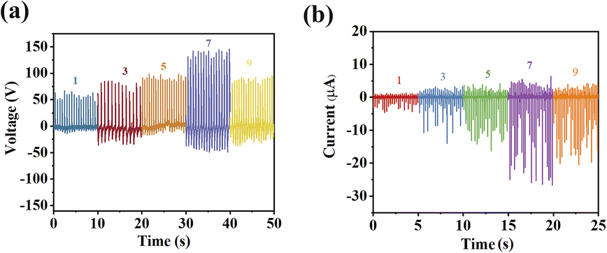
Because the concentration of 1 in the composite film is a critical factor in device performance, the number of spin-coating cycles was utilized to regulate its content within the film. Fig. 4 displays the open-circuit voltage (Voc) and short-circuit current (Isc) of 1@S-PDMS(800#) across various spin coating cycles. These measurements were taken by applying a consistent pressure of approximately 20 N to their surfaces using palm pressure. When the spin-coating cycle is set to one, the Voc is 50 V and the Isc is 3.8 μA. As the spin-coating cycles increase to 3, 5, and 7, device performance improves. At 7 cycles, Voc and Isc reach their peak values of 120 V and 25 μA, respectively. However, at 9 cycles, there is a decrease in device performance, with Voc dropping to 75 V and Isc to 20 μA. A similar trend in Voc and Isc was also observed in other devices, i.e., 1@S-PDMS(600#), 1@S-PDMS(1200#) and 1@S-PDMS(1500#) (Fig. S11†). The optimal performance of the devices at seven spin-coating cycles can be attributed to the gradual increase in the content of 1 within the film as the number of cycles increases. However, when the spin-coating cycles exceed seven, despite the continuing increase in the content of 1, it begins to aggregate, as illustrated in Fig S12.† This aggregation leads to enhanced dielectric constants and Maxwell–Wagner–Sillars polarization,33,34 and consequently, a high content of 1 would degrade rather than enhance the piezoelectric response.
 | ||
| Fig. 4 V oc (a) and Isc (b) for 1@S-PDMS(800#) with different spin coating cycles with palm pressure. | ||
For comparison, four devices with distinct structures but identical sizes to 1@S-PDMS were prepared, i.e., (1) Flat-PDMS film, which lacks a micropore structure on its surface; (2) S-PDMS, featuring micropores on its surface; (3) 1–Flat-PDMS, where 1 is dispersed within the bulk of the Flat-PDMS film; and (4) 1–S-PDMS, where 1 is dispersed within the bulk of the S-PDMS film. The devices of each distinct structure with the best performance were chosen for comparison (under 20 N palm pressure) (Fig. S13†). As demonstrated in Fig. 5, the performance of S-PDMS, 1–Flat-PDMS and 1–S-PDMS is notably superior to that of Flat-PDMS, yet significantly inferior to that of 1@S-PDMS. Notably, S-PDMS exhibits a distinct output signal with a Voc of 35 V and an Isc of 5 μA, likely due to its unique surface structure. This structure features a layer of micropores between the electrodes, which introduces a triboelectric response.35 Distinctly, the remarkable performance of 1@S-PDMS stems from the synergistic interplay between its piezoelectric and triboelectric responses (Fig. S14†).36,37 When 1 is embedded within the micropores on the surface of PDMS, rather than within its bulk, the surface microstructure facilitates uniform dispersion of 1 and prevents aggregation. Additionally, under mechanical pressure, 1 can easily induce piezoelectric charges on the surface of S-PDMS.38
 | ||
| Fig. 5 V oc (a) and Isc (b) for various devices with different constructions at 20 N palm pressure. | ||
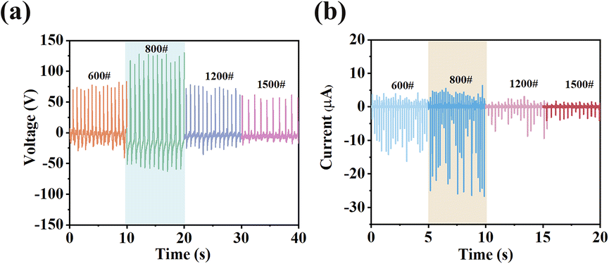
Given the critical importance of the surface microstructure, we conducted further investigations into the effects of surface microstructures with varying pore sizes on device performance. Comparing the optimal output performance of four types of 1@S-PDMS devices with varying pore sizes (Fig. 6) (where the number of spin-coating cycles was maintained at seven as previously discussed and the pressure applied to the device was 20 N), the device of 1@S-PDMS(1500#) exhibited the poorest performance. A clear trend emerged, showing enhanced performance with increasing pore sizes within S-PDMS. The device with a pore size of 800# (1@S-PDMS(800#)) delivered the best performance. However, further increasing the pore size beyond 800# led to a decline in performance. To elucidate this unique effect of pore size, the triboelectric performance of the S-PDMS blank across varying pore sizes was investigated. As shown in Fig. S15,† the triboelectric performance of the S-PDMS blank improves as the pore size increases, peaking when the pore size reaches 800#. And as the pore size continued to increase, the performance decreased. Typically, a decrease in micropore size typically leads to an increase in effective surface area, which in turn enhances device performance.39 But the surface roughness is also a critical factor of triboelectricity. The improvement in the triboelectric performance of the S-PDMS blank as the pore size increases can be attributed to an increase in surface roughness.35 Thus, the most optimal performance exhibited by 1@S-PDMS(800#) is due to the synergistic interplay between piezoelectricity and triboelectricity.
 | ||
| Fig. 6 V oc (a) and Isc (b) for 1@S-PDMS with different micropore sizes. | ||
Fig. S16† presents the power density for 1@S-PDMS(800#) and 1–Flat-PDMS. The power density for 1@S-PDMS(800#) peaks at approximately 490 μW cm−2 with a load resistance of 7 MΩ, whereas 1–Flat-PDMS achieves only a maximum of 41 μW cm−2. Because the maximum power density for 1@S-PDMS(800#) is 12 times that of 1–Flat-PDMS, this result clearly indicates that the device's microstructure plays a crucial role in enhancing its performance. It is worth mentioning that while the power density of 1@S-PDMS is lower than that reported for the single crystal-array device of C6H5N(CH3)3CdBr2Cl0.75I0.25-PDMS (1100 μW cm−2)26 and ultrasonic response power density of PVDF/TMCM-MnCl3 (1020 μW cm−2),40 the power density of 1@S-PDMS(800#) is not only comparable to that of V-NaNbO3-PDMS (480 μW cm−2),41 but also surpasses the power densities of all reported molecule-based energy harvesting devices, such as 115 μW cm−2 of TMCMCdCl3-PDMS33 and 74 μW cm−2 of MASnBr3-PDMS (Table S3†).20
Applications in human physiological signal monitoring
To assess the potential of 1@S-PDMS(800#) as a flexible pressure sensor, the output signals of the sensor under various stresses (Fig. S17†) were performed. Based on these data, the sensor's sensitivity at various stress levels was obtained as shown in Fig. 7. The output voltage increases proportionally with stress up to 24 kPa, after which this trend slows down. Beyond 45 kPa, the output voltage remains essentially constant, likely due to the theoretical limitations of effective strain in piezoelectric materials at high pressure.42,43 According to the data in Fig. 7, the sensitivity of the sensor is 3.57 V kPa−1 below 24 kPa and 1.02 V kPa−1 in the range of 24 kPa to 45 kPa. Although this sensitivity is lower than the highest reported value for PVDF-based PVDF/TMCM-MnCl3 (6.21 V kPa−1),40 it is still the second highest sensitivity reported for molecule-based sensors to date (Table S4†). The stability of the 1@S-PDMS(800#) sensor was also evaluated under both low (10 kPa) and high (70 kPa) palm stresses (Fig. S18†). After hundreds or even thousands of cycles, the device shows no signs of performance degradation, indicating that the sensor exhibits excellent stability under both low and high stresses.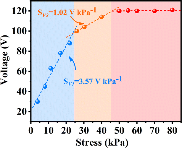 | ||
| Fig. 7 The sensitivity of the sensor under various stresses. | ||
Given the excellent sensing properties of 1@S-PDMS(800#), it was employed to detect pressure signals generated by physiological processes in the human body. Fig. 8a illustrates that when the finger joint bends at angles of 45° and 90°, it produces voltage peaks of up to 1.02 V and 2.94 V, respectively. When the finger joint is bent repeatedly four times, the sensor consistently delivers four sets of signals with identical waveforms and values, demonstrating the sensor's stable and reliable performance.30 Similarly, we attach sensors to the wrist that can detect movements from clenching to opening of the palm (Fig. 8b). Fig. 8c and d illustrate speech signals originating from the movement of laryngeal muscles and the vibration of vocal cords. The signal shape remains consistent, demonstrating the sensor's robust performance. Even when the word is read at varying volumes, only the peak value of the signal fluctuates, while the waveforms stay unchanged. This highlights the sensor's ability to detect minute pressures from acoustic vibrations.44 Furthermore, the sensor is capable of recognizing distinct words; for example, when pronouncing “Xia Men” and “Hua Xue Hua Gong”, the voltage waveforms exhibit double peaks and multiple sets of double peaks, respectively (Fig. 8d). Additionally, the sensor was placed inside a face mask to monitor the wearer's breathing rate, serving as a valuable tool for assessing health—a task that has become particularly important in the post-pandemic era. As shown in Fig. S19,† the average breathing rate of the subjects was 3.0 seconds, comfortably within the normal range of 3 to 5 seconds per breath. The voltage waveforms display excellent stability and clearly distinguish each breath, underscoring the sensor's capability to detect the frequency of weak signals from breathing.
 | ||
| Fig. 8 (a) Signal from bending the knuckles. (b) Signal from clenching the palm. (c) Recognition of the word “chemistry” at different volumes. (d) Recognition of the Chinese words “Xia Men” and “Hua Xue Hua Gong”. | ||
Conclusions
In summary, we have developed a molecule-based ferroelectric 1, with a piezoelectric constant d33 of 331 pC N−1. Notably, the power density of the composite piezoelectric sensor device 1@S-PDMS(800#) is twelve times that of 1–Flat-PDMS, underscoring the critical role of microstructures in enhancing performance. This improvement is attributed to a synergistic combination of piezoelectric and triboelectric effects. As a flexible pressure sensor, 1@S-PDMS(800#) effectively detects human physiological signals, such as finger bending, breathing, and speech recognition, without the need for an external power supply. Given that the power density of 1@S-PDMS(800#) surpasses the power densities of all reported molecule-based energy harvesting devices (excluding single-crystal array devices and ultrasound-driven PVDF/TMCM-MnCl3 devices) and boasts the second highest sensitivity reported for molecule-based sensors to date, this work not only advances the practical applications of molecule-based piezoelectric materials but also explores their potential in self-powered sensing applications.Experimental
Preparation
All the chemical solvents and reagents were employed without further purification. All spin-coating operations were conducted using a KW-4A spin coater from the Institute of Microelectronics, Chinese Academy of Sciences.Initially, 5 mmol of gallium(III) oxide was dissolved in 40% HBr at 130 °C. Subsequently, 10 mmol of (2-bromoethyl) trimethylammonium bromide was added and dissolved via reflux condensation, resulting in a clear orange solution. After approximately one week of evaporation, orange block crystals of 1 were obtained, with a total yield of 92% based on (2-bromoethyl) trimethylammonium bromide. To produce a powdered form of 1, the mixed solution was evaporated at 100 °C, and the resulting powder was washed three times with absolute ethanol.
Fabrication of sensor devices
The base polymer of PDMS (part A), curing agent (part B), and toluene were mixed in a 10![[thin space (1/6-em)]](https://www.rsc.org/images/entities/char_2009.gif) :1:11 ratio and stirred to produce the PDMS solution. This solution was then evenly dispersed in either a Teflon evaporator or Teflon evaporator lined with sandpaper of varying coarseness (P600, P800, P1200, and P1500, where ‘P’ is the roughness class of sandpaper) on the bottom. The 1@S-PDMS composite films were fabricated as follows: a 1 mol per L [(CH3)3NCH2CH2Br][GaBr4] aqueous solution was prepared by dissolving 5 mmol of 1 in 5 mL of deionized water. S-PDMS was applied to the silicon substrate, and 100 μL of the [(CH3)3NCH2CH2Br][GaBr4] solution was dispersed onto S-PDMS using a micropipette and spun at 1500 rpm for 30 seconds. Subsequently, 1 mL of isopropanol was added, and the sample was then spun at 2500 rpm for 1 minute. This spin-coating process was repeated for a varying number of cycles. Finally, S-PDMS was heated on a 100 °C hot plate for 1 hour to obtain 1@S-PDMS.
:1:11 ratio and stirred to produce the PDMS solution. This solution was then evenly dispersed in either a Teflon evaporator or Teflon evaporator lined with sandpaper of varying coarseness (P600, P800, P1200, and P1500, where ‘P’ is the roughness class of sandpaper) on the bottom. The 1@S-PDMS composite films were fabricated as follows: a 1 mol per L [(CH3)3NCH2CH2Br][GaBr4] aqueous solution was prepared by dissolving 5 mmol of 1 in 5 mL of deionized water. S-PDMS was applied to the silicon substrate, and 100 μL of the [(CH3)3NCH2CH2Br][GaBr4] solution was dispersed onto S-PDMS using a micropipette and spun at 1500 rpm for 30 seconds. Subsequently, 1 mL of isopropanol was added, and the sample was then spun at 2500 rpm for 1 minute. This spin-coating process was repeated for a varying number of cycles. Finally, S-PDMS was heated on a 100 °C hot plate for 1 hour to obtain 1@S-PDMS.
For composite films with 1 dispersed in the bulk of PDMS, 1 was dispersed in the PDMS solutions at varying mass fractions, referred to as 1–Flat-PDMS. Similarly, 1 was dispersed in S-PDMS, referred to as 1–S-PDMS. The prepared solutions were evenly spread in a Teflon evaporator (diameter = 60 mm) and subsequently cured. All types of composite films were then covered with conductive tape on both the top and bottom surfaces, serving as electrodes in the fabricated sensor devices (the active areas are 2 × 2 cm2).
Data availability
The data supporting this article have been included as part of the ESI.†Author contributions
Z. X. Tang fabricated the devices and performed electrical property measurement work. B. Wang synthesized the compounds, and Z. R. Li carried out d33 measurement and conducted the X-ray crystallographic analysis and PXRD measurement. Z. Huang conducted the SHG measurement. H. X. Zhao, L. S. Long and L. S. Zheng conceptualized the work and wrote the paper.Conflicts of interest
There are no conflicts to declare.Acknowledgements
This work was supported by the National Natural Science Foundation of China (Grant No. 22371235, 92361301 and 92161203).Notes and references
- K. S. Ramadan, D. Sameoto and S. Evoy, Smart Mater. Struct., 2014, 23, 033001 CrossRef CAS.
- M. T. Chorsi, E. J. Curry, H. T. Chorsi, R. Das, J. Baroody, P. K. Purohit, H. Ilies and T. D. Nguyen, Adv. Mater., 2019, 31, 1802084 CrossRef.
- M. Huang, M. Zhu, X. Feng, Z. Zhang, T. Tang, X. Guo, T. Chen, H. Liu, L. Sun and C. Lee, ACS Nano, 2023, 17, 6435 CrossRef CAS.
- T. M. Guo, Y. J. Gong, Z. G. Li, Y. M. Liu, W. Li, Z. Y. Li and X. H. Bu, Small, 2022, 18, 2103829 CrossRef CAS PubMed.
- H. Chen, L. Zhou, Z. Fang, S. Wang, T. Yang, L. Zhu, X. Hou, H. Wang and Z. L. Wang, Adv. Funct. Mater., 2021, 31, 2011073 CrossRef.
- S. Mondal, T. Paul, S. Maiti, B. K. Das and K. K. Chattopadhyay, Nano Energy, 2020, 74, 104870 CrossRef.
- B. B. Ma, L. Cheng, S. B, X. F. Jia, J. Ma, J. l. Zhao, L. F. Wang and Y. Qin, Nano Energy, 2023, 111, 108412 CrossRef.
- W. Z. Song, X. X. Wang, H. J. Qiu, N. Wang, M. Yu, Z. Y. Fan, S. Ramakrishna, H. Hu and Y. Z. Long, Nano Energy, 2021, 82, 105695 CrossRef.
- S. Y. Huang, Y. J. Gao, Y. Hu, F. Y. Shen, Z. S. Y. Jin and Y. Cho, RSC Adv., 2023, 13, 29174 RSC.
- W. L. Deng, Y. H. Zhou, A. Libanori, G. R. Chen, W. Q. Yang and J. Chen, Chem. Soc. Rev., 2022, 51, 3380 RSC.
- T. Vijayakanth, D. J. Liptrot, E. Gazit, R. Boomishankar and C. R. Bowen, Adv. Funct. Mater., 2022, 32, 2109492 CrossRef CAS.
- Q. Xu, Z. Wang, J. Zhong, M. Yan, S. Zhao, J. Gong, K. Feng, J. Zhang, K. Zhou, J. Xie, H. Xie, D. Zhang, Y. Zhang and C. Bowen, Adv. Funct. Mater., 2023, 33, 2304402 CrossRef CAS.
- X. L. Cao, Y. Xiong, J. Sun, X. X. Zhu, Q. J. Sun and Z. L. Wang, Adv. Funct. Mater., 2021, 31, 2102983 CrossRef CAS.
- B. Stadlober, M. Zirkl and M. Irimia-Vladu, Chem. Soc. Rev., 2019, 48, 1787 RSC.
- Y. Qin, F. F. Gao, S. Qian, T. M. Guo, Y. J. Gong, Z. G. Li, G. D. Su, Y. Gao, W. Li, C. Jiang, P. Lu and X. H. Bu, ACS Nano, 2022, 16, 3221 CrossRef.
- S. Deswal, S. K. Singh, R. Pandey, P. Nasa, D. Kabra, B. Praveenkumar, S. Ogale and R. Boomishankar, Chem. Mater., 2020, 32, 8333 CrossRef.
- S. Deswal, S. K. Singh, P. Rambabu, P. Kulkarni, G. Vaitheeswaran, B. Praveenkumar, S. Ogale and R. Boomishankar, Chem. Mater., 2019, 31, 4545 CrossRef.
- B. Wang, Z. R. Li, Z. X. Tang, H. X. Zhao, L. S. Long and L. S. Zheng, Chem. Sci., 2024, 15, 15192 RSC.
- T. Vijayakanth, A. K. Srivastava, F. Ram, P. Kulkarni, K. Shanmuganathan, B. Praveenkumar and R. Boomishankar, Angew. Chem., Int. Ed., 2018, 57, 9054 CrossRef PubMed.
- S. Ippili, V. Jella, J. Kim, S. Hong and S. G. Yoon, ACS Appl. Mater. Interfaces, 2020, 12, 16469 CrossRef.
- W. Q. Liao, D. Zhao, Y. Y. Tang, P. F. Zhang, Y. Li, P. P. Shi, X. G. Chen, Y. M. You and R. G. Xiong, Science, 2019, 363, 1206 CrossRef CAS PubMed.
- G. Huang, A. A. Khan, M. M. Rana, C. Xu, S. Xu, R. Saritas, S. Zhang, E. Abdel-Rahmand, P. Turban, S. Ababou-Girard, C. Wang and D. Ban, ACS Energy Lett., 2021, 6, 16 CrossRef.
- X. G. Chen, X. J. Song, Z. X. Zhang, P. F. Li, J. Z. Ge, Y. Y. Tang, J. X. Gao, W. Y. Zhang, D. W. Fu, Y. M. You and R. G. Xiong, J. Am. Chem. Soc., 2020, 142, 1077 CrossRef PubMed.
- Q. Pan, Y. A. Xiong, T. T. Sha and Y. M. You, Mater. Chem. Front., 2021, 5, 44 RSC.
- B. Wang, J. F Hong, Y. T. Yang, H. X. Zhao, L. S. Long and L. S. Zheng, Matter, 2022, 5, 1296 CrossRef.
- Y. Hu, K. Parida, H. Zhang, X. Wang, Y. X. Li, X. Zhou, S. A. Morris, W. H. Liew, H. Wang, T. Li, P. S. Lee and H. J. Fan, Nat. Commun., 2022, 13, 5607 CrossRef.
- W. R. Li, C. H. Li, G. Zhang, L. K. Li, K. Huang, X. T. Gong, C. Zhang, A. Zheng, Y. X. Tang, Z. Z. Wang, Q. L. Tong, W. Dong, S. L. Jiang, S. L. Zhang and Q. Wang, Adv. Mater., 2021, 33, 2104107 CrossRef PubMed.
- Q. Pan, Z. X. Gu, R. J. Zhou, Z. J. Feng, Y. A. Xiong, T. T. Sha, Y. M. You and R. G. Xiong, Chem. Soc. Rev., 2024, 53, 5781 RSC.
- V. Jella, S. Ippili, J. H. Eom, S. V. N. Pammi, J. S. Jung, V. D. Tran, V. H. Nguyen, A. Kirakosyan, S. Yun, D. Kim, M. R. Sihn, J. Choi, Y. J. Kim, H. J. Kim and S. G. Yoon, Nano Energy, 2019, 57, 74 CrossRef.
- U. Pierre Claver and G. Zhao, Adv. Eng. Mater., 2021, 23, 2001187 CrossRef.
- P. K. Panda, B. Sahoo, T. S. Thejas and M. Krishna, J. Electron. Mater., 2022, 51, 93 CrossRef.
- G. H. Haertling, J. Am. Ceram. Soc., 1999, 82, 797 CrossRef.
- Y. J. Gong, Z. G. Li, H. Chen, T. M. Guo, F. F. Gao, G. J. Chen, Y. Zhang, Y. M. You, W. Li, M. He, X. H. Bu and J. Yu, Matter, 2023, 6, 2066 CrossRef.
- B. Wang, H. Wu, W. Hou, Z. Fang, H. Liu, F. Huang, S. Li and H. Zhang, J. Mater. Chem. A, 2023, 11, 23498 RSC.
- H. Zhu, J. Liang, W. Long, F. Zeng, X. Zhang and Z. Chen, J. Mater. Chem. C, 2024, 12, 1782 RSC.
- S. Hajra, A. M. Padhan, B. K. Panigrahi, P. Pakawanit, Z. Jagličić, N. Vittayakorn, Y. K. Mishra, S. Lee and H. J. Kim, J. Materiomics, 2024, 10, 792 CrossRef.
- M. Sahu, V. Vivekananthan, S. Hajra, D. K. Khatua and S. J. Kim, Appl. Mater. Today, 2021, 22, 100900 CrossRef.
- Z. Wang, Z. Liu, G. Zhao, Z. Zhang, X. Zhao, X. Wan, Y. Zhang, Z. L. Wang and L. Li, ACS Nano, 2022, 16, 1661 CrossRef.
- M. S. U. Rasel and J. Y. Park, Appl. Energy, 2017, 206, 150 CrossRef.
- P. Chen, C. Cheng, X. M. Yang, T. T. Sha, X. H. Zou, F. C. Zhang, W. Jiang, Y. Xu, X. B. Cao, Y. M. You and Z. Q. Luo, ACS Nano, 2023, 17, 25625 CrossRef.
- M. V. Paranjape, J. Kim, Y. Kim, E. Jo, S. A. Graham, P. Manchi, J. K. Lee and J. S. Yu, Compos. Sci. Technol., 2023, 242, 110195 CrossRef.
- J. B. Yu, L. Chen, X. J. Hou, J. L. Mu, J. He, W. P. Geng, X. J. Qiao and X. J. Chou, J. Materiomics, 2022, 8, 247 CrossRef.
- J. Palosaari, M. Leinonen, J. Hannu, J. Juuti and H. Jantunen, J. Electroceram., 2012, 28, 214 CrossRef.
- Y. Long, Z. Wang, F. Xu, B. Jiang, J. F. Xiao, J. Yang, Z. L. Wang and W. G. Hu, Small, 2022, 18, 2203956 CrossRef.
Footnote |
| † Electronic supplementary information (ESI) available: Measurements and methods, TGA, DSC, PXRD, SHG, d33 measurement, SEM, Voc, Isc, theoretical Ps value calculation, crystal data and the additional tables. CCDC 2208701. For ESI and crystallographic data in CIF or other electronic format see DOI: https://doi.org/10.1039/d4sc05442c |
| This journal is © The Royal Society of Chemistry 2024 |