
 Open Access Article
 This Open Access Article is licensed under a Creative Commons Attribution-Non Commercial 3.0 Unported Licence
Encapsulation of crystalline and amorphous Sb2S3 within carbon and boron nitride nanotubes†
Griffin M.
Milligan
 a,
Dmitri Leo Mesoza
Cordova
a,
Ze-Fan
Yao
b,
Brian Y.
Zhi
a,
Lyndsey R.
Scammell
c,
Toshihiro
Aoki
d and
Maxx
Arguilla
*a
a,
Dmitri Leo Mesoza
Cordova
a,
Ze-Fan
Yao
b,
Brian Y.
Zhi
a,
Lyndsey R.
Scammell
c,
Toshihiro
Aoki
d and
Maxx
Arguilla
*a
aDepartment of Chemistry, University of California Irvine, Irvine, California 92697, USA. E-mail: marguill@uci.edu
bDepartment of Chemical and Biomolecular Engineering, University of California Irvine, Irvine, California 92697, USA
cBNNT LLC, 300 Ed Wright Lane Suite A, Newport News, Virginia 23606, USA
dIrvine Materials Research Institute, University of California Irvine, Irvine, California 92697, USA
First published on 3rd June 2024
Abstract
The recent rediscovery of 1D and quasi-1D (q-1D) van der Waals (vdW) crystals has laid foundation for the realization of emergent electronic, optical, and quantum-confined physical phenomena in both bulk and at the nanoscale. Of these, the highly anisotropic q-1D vdW crystal structure and the visible-light optical/optoelectronic properties of antimony trisulfide (Sb2S3) have led to its widespread consideration as a promising building block for photovoltaic and non-volatile phase change devices. However, while these applications will greatly benefit from well-defined and sub-nanometer-thick q-1D structures, little has been known about feasible synthetic routes that can access single covalent chains of Sb2S3. In this work, we explore how encapsulation in single or multi-walled carbon nanotubes (SWCNTs or MWCNTs) and visible-range transparent boron nitride nanotubes (BNNTs) influences the growth and phase of Sb2S3 nanostructures. We demonstrate that nanotubes with smaller diameters had a more pronounced effect in the crystallographic growth direction and orientation of Sb2S3 nanostructures, promoting the crystallization of the guest structures along the long-axis [010]-direction. As such, we were able to reliably access well-ordered few to single covalent chains of Sb2S3 when synthesized within defect-free SWCNTs with sub-2 nm inner diameters. Intriguingly, we found that the degree of crystalline order of Sb2S3 nanostructures was strongly influenced by the presence of defects and discontinuities along the Sb2S3-nanotube interface. We show that amorphous nanowire domains of Sb2S3 form around defect sites in larger, multi-walled nanotubes that manifest inner wall defects and discontinuities, suggesting a means to manipulate the crystallization dynamics of confined sub-10 nm-thick Sb2S3 nanostructures within nanotubes. Lastly, we show that ultranarrow amorphous Sb2S3 can impart functionality onto isolable BNNTs with photocurrent generation in the pA range which, alongside the dispersibility of the Sb2S3@BNNTs, could be leveraged to easily fabricate photoresistors only a few nm in width. Altogether, our results serve to solidify the understanding of how q-1D vdW pnictogen chalcogenides crystallize within confined synthetic platforms and are a step towards realizing functional materials from ensembles of encapsulated heterostructures.
1 Introduction
Recent years have seen a drastic uptick in the synthesis and characterization of atomically precise low-dimensional crystals that approach the single-atom-thick regime. Such studies have led to the discovery and rediscovery of many useful two-dimensional (2D),1–3 one-dimensional (1D), and quasi-one-dimensional (q-1D) van der Waals (vdW)4,5 materials with nascent physical properties. The anisotropy inherent in the structure of these materials has enabled the development of facile top-down exfoliation6–9 or bottom-up growth10–13 methods to achieve sub-10 nm nanocrystals with tunable morphologies such as nanosheets, nanoribbons, and nanowires, and shape- or dimension-dependent properties. This structural and chemical tunability has led to discoveries including the transition from indirect band gap in the bulk to direct band gap in monolayer MoS2 (ref. 14) and the quantum spin Hall effect in graphene in 2D.15 Morphological tunability in 1D, on the other hand, has led to discoveries including an enhanced intrinsic photovoltaic effect in TaS3,16 high coercivity in CrSbSe3,17 high breakdown current in TaSe3,18 high-fidelity transport in (TaSe4)2I,19 and the approach of an indirect-to-direct band gap crossover in ultrathin Sb2S3 nanowires.13 The latter material, antimony trisulfide, has been at the forefront of q-1D vdW materials research not only as a model structural phase but also due to its unique optoelectronic and structural properties arising from its anisotropic q-1D structure and visible-light optical properties. This earth abundant material is found in nature as the mineral stibnite20,21 and as the amorphous mineraloid metastibnite.22 In more recent times, it has gained significant interest as a potential thin film photovoltaic material with a tunable band gap between 1.6–2.85 eV,23–27 high predicted power conversion efficiency in tandem cells,28,29 and a high absorption coefficient (α > 104 cm−1).30 Moreover, it has been demonstrated that Sb2S3 is also a phase change material (PCM),25,31 as the crystalline (c-Sb2S3) and amorphous (a-Sb2S3) phases that can be interconverted thermally or optically, with broad ranging implications for use in optical switching, tunable emitters/absorbers, and, in particular, non-volatile data storage.32,33 This class includes other pnictogen- and tetrel-based chalcogenide materials often based on antimony and/or germanium, including Sb2Se3,31 Ge2Sb2Te5,34 Ge20Sb20S20Se20Te20,35 Ge15Sb40,S15Se15Te15,36 and many others.From a structural standpoint, Sb2S3 is a q-1D vdW material comprised of sub-nanometer-thick ribbons of [Sb4S6]n that infinitely extend in one direction along the crystallographic b-axis ([010]-direction) and are held together along the other two axes (basal plane) by weak vdW forces.20 Yet, these forces are not equal along various crystallographic axes. The terminal trivalent Sb atoms along the [Sb4S6]n chain (in contrast to the pentavalent core Sb atoms) express stereochemically active lone pairs which interact with the electronegative S atoms terminating the neighboring ribbon. This results in a binding interaction along the c-axis ([001]-direction) that is approximately double that of the interaction along a-axis ([100]-direction).37 The stereochemical activity of this lone pair has been found to stem from the Sb 5s orbital mixing with S 3p orbitals to express bonding anisotropy in the anti-bonding state. Beyond its implications to the optical and electronic properties of Sb2S3, it was also demonstrated that these anisotropic bonding motifs can be leveraged to control the nanoscale morphology of Sb2S3 nanocrystals. Top-down approaches like mechanical and solvent exfoliation of a bulk stibnite crystal are known to cleave the crystal predominantly along the weakest a-axis direction and result in 2D nanosheets and ribbons,38,39 rather than 1D nanowires as one might expect from the underlying q-1D lattice. To some extent, the differing electronic interactions can also be leveraged in bottom-up growth to direct the crystallization of Sb2S3 nanostructures by tuning the precursor concentration and temperature with vapor phase growth, allowing access to a variety of morphologies such as nanowires, nanoribbons, and nanosheets from the same [Sb4S6]n chain building blocks but with differing optical properties and electronic structures.13 Additionally, in single covalent chains of Sb2S3, computational predictions of a rare indirect-to-direct gap transition in 1D and q-1D vdW semiconductors, in addition to a tightly bound excitonic state, have been demonstrated.40 Experimentally, nanowires display an emission distinct from bulk Sb2S3 at and below 100 nm in diameter.13 Despite the tremendous efforts towards growing nanoscale structures of Sb2S3,41–43 a reliable methodology enabling the isolation of single covalent chains of crystalline Sb2S3 by any existing top-down or bottom-up approach—and one that is not obscured by the anisotropic inter-chain interactions arising from stereochemically-active lone pairs—has remained elusive.
Encouragingly, an effective method that directly influences the diameter of nanowire growth down to sub-nanometer thickness is via nanotube encapsulation.44,45 In this method, pre-grown nanotubes with open ends are used as nanoscale reaction vessels, into which materials of interest migrate via capillary action in melt or vapor phase.45 For the purpose of our report, these materials are denoted as material@NT. In the spectrum of well-defined nanotube encapsulants, carbon nanotubes (CNTs) are the best understood, with many fundamental studies offering insight into the structure of confined and metastable materials. For example, many optically-active semiconducting materials have been encapsulated in ultranarrow carbon nanotubes, including single NbSe3 chains,46 narrow direct gap IV–VI materials like SnSe,47 SnTe,48 and PbTe,49 and more recently lead halide perovskites.50,51 Still, despite these efforts, material@CNT heterostructures are generally limited to structural observations due to the metallic/low band gap52,53 and high absorbance54,55 of the nanotube meaning conductivity and optical signal of the host material is completely occluded by the CNT. Alternatively, the visible-range transparent and electrically insulating nature56–59 of boron nitride nanotubes (BNNTs)60 facilitates the straightforward measurement of optoelectronic properties in material@BNNT heterostructures.61 These heterostructures are less studied and are, so far, limited to molecular filling with organic dyes62,63 or nanoparticle/rod filling61,64–69 apart from few studies which involved Te@BNNT,70 NbSe3@BNNT,46 and KX@BNNT (X = Cl, Br, I)71 which are the only extended structures encapsulated within BNNTs to the best of our knowledge. Leveraging the properties of BNNTs is essential to translate the potential of nanotube encapsulation to the fundamental understanding of optical properties of encapsulated materials and to realize practical application in electronic and photonic devices. More generally, the utility of diverse nanotubes in terms of structure (carbon versus boron nitride) and sizes (various diameters and number of walls) could provide a means to further understand how the immediate chemical and structural environment within nanotubes (e.g. defects) play a role in the structure and phase of guest materials in materials@NTs.
In this report, we detail the encapsulation of Sb2S3 within nanotubes of various diameters and chemical compositions with the goal of understanding the limit of structural confinement of Sb2S3 when encapsulated within NTs and how the resulting size, structure, and degree of crystallinity influence the properties of the resulting Sb2S3@NTs. In smooth, defect-free single walled CNTs (SWCNTs), we obtained few to single covalent chains of c-Sb2S3 with a high filling efficiency. Yet, using other nanotube sources, we found that the degree of crystallinity of the Sb2S3 is heavily dependent on the surface roughness of the nanotube it interfaces with, evidenced by high resolution transmission electron microscopy (HRTEM) and complemented by Raman spectroscopy. This is most pronounced in BNNTs, where we primarily observed a-Sb2S3 filling around nanotube defects (pinches, kinks, BN aggregates) with crystal formation only appearing where the nanotubes were especially smooth. Likewise, we demonstrate that this is also the case in MWCNTs with larger diameters which also contained defects within the inner surface. We generally observed that the amorphization is driven by the surface smoothness rather than the host–guest chemistry between Sb2S3 and the BNNT or MWCNT. Moreover, we found that the amorphization/defect ratio is dependent on the nanotube diameter, suggesting that it is driven by the interfacial stability of the amorphous phase compared to the crystalline Sb2S3 phase. Finally, we observe emergent optical properties of a-Sb2S3@BNNT, including a visible range absorption at 502 nm/2.47 eV consistent with the optical signatures of a-Sb2S3 thin films and a pronounced photocurrent response demonstrating that BNNTs can be sensitized by the guest a-Sb2S3 phase.
2 Results and discussion
We achieved the encapsulation of Sb2S3 in single walled carbon nanotubes (SWCNTs) via a mixed melt growth process using SWCNTs with opened ends (annealed in air 420 °C 5 hours) and a large excess of pre-synthesized, phase-pure, Sb2S3 powder (Fig. S1†) heated above its melting point at 600 °C. In a mixed-melt growth of this type, it is generally considered that capillary action drives liquid Sb2S3 melt into the nanotubes. As the reaction ampoule cools, the encapsulated Sb2S3 crystallizes within the nanotubes.45 Once synthesized, we used high-resolution transmission electron microscopy (HRTEM) and scanning transmission electron microscopy (STEM) to evaluate the success and resulting quality of the nanotube filling. By our direct observations in HRTEM, we could readily access Sb2S3@SWCNT at a high filling efficiency as all SWCNTs that we found were filled with the guest phase (Fig. 1A). As expected of the q-1D vdW structure of Sb2S3, the covalent axis was determined to align parallel to the long axis of the nanotube, with a measured d spacing of 1.9 Å which corresponds to the [020]-direction of the native Sb2S3 structure d(020) = 1.918 Å (Fig. 1A and C). This indicates that Sb2S3 has a propensity to crystallize along the long-chain covalent axis direction strongly influenced by the direction of the confined 1D nanotube. The consistency of the d-spacing with the native structure also indicates that minimal distortion was caused by the confinement. Energy dispersive X-ray spectroscopy (EDS) mapping performed with 80 kV annular dark-field (ADF) STEM also confirmed the identity of the phase, with an apparent ratio of 2![[thin space (1/6-em)]](https://www.rsc.org/images/entities/char_2009.gif) :3 Sb/S within the SWCNTs (Fig. 1B). As we saw previously with our work on Sb2Se3,72 this method of confinement within SWCNTs accessed ultrathin nanowires of Sb2S3 within nanotubes of fewer than 2 nm, meaning that only 1–2 covalent chains with 1.04 nm distance between terminal sulfur atoms could occupy a given nanotube.
:3 Sb/S within the SWCNTs (Fig. 1B). As we saw previously with our work on Sb2Se3,72 this method of confinement within SWCNTs accessed ultrathin nanowires of Sb2S3 within nanotubes of fewer than 2 nm, meaning that only 1–2 covalent chains with 1.04 nm distance between terminal sulfur atoms could occupy a given nanotube.
 | ||
| Fig. 1 Sb2S3 encapsulated within SWCNTs. (A) HRTEM of Sb2S3@SWCNTs. (B) 80 kV Cs-corrected DF-STEM and EDS mapping of Sb2S3@SWCNTs. (C) Model structure of a single covalent Sb2S3 ribbon within a (21,0) carbon nanotube. For clarity, the SWCNT is shown as a skeletal model in the in-plane projection. (D) Raman spectra of Sb2S3@SWCNTs, Sb2S3, and SWCNTs. (E) DRS of Sb2S3@SWCNTs, Sb2S3, and SWCNTs. | ||
We performed Raman spectroscopy to further verify that minimal structural modulation had occurred as was observed by HRTEM imaging (Fig. 1D). Firstly, Raman signals from both c-Sb2S3 and empty SWCNTs are in close agreement with literature values.24,73 Sb2S3 contained five well-resolved peaks: 193 cm−1, 246 cm−1, 280 cm−1, 302 cm−1, and 309 cm−1, with the two Ag signals occurring at 280 and 309 cm−1 being the most prominent. In the region that we surveyed, the SWCNTs contained only radial breathing mode (RBM) signals.74–76 The most intense radial breathing mode also occurred at the highest wavenumber, 181 cm−1, before the signals abruptly ceased at the higher wavenumber region of the spectra. Raman spectroscopy revealed minute, though obvious, differences between the filled and empty SWCNTs. A broad feature centered around 266 cm−1 that is well above the highest radial breathing mode intensity emerged with a shoulder intensity around 310 cm−1. We assign this broad feature to the two Ag modes of Sb2S3 that are broadened significantly and red-shifted from confinement effects. The highest SWCNT RBM peak, however, remained centered at approximately 180 cm−1. This is in contrast with our work on Sb2Se3@SWCNT, where the observable Ag mode of Sb2Se3 did not shift and is indicative of a more pronounced confinement effect or nanotube-guest interaction. We note that, while the red-shifted Ag mode is low intensity and broad which makes it highly susceptible to background noise, this observed peak difference (Δ = 14 cm−1) is far too considerable to attribute to noise alone. The well-resolved Raman peaks also enabled us to evaluate the SWCNT graphitic signals. From these, we found little-to-no difference in the G−-band or G+-band, which is suggestive that the SWCNT itself was not distorted significantly (Fig. S4†).
As with other nanotube-encapsulated crystalline phases, the successful encapsulation of single covalent chains of Sb2S3 within SWCNTs prompted us to investigate the evolution of the optical properties of bulk Sb2S3 compared to Sb2S3@SWCNT. To this end, we obtained the Kubelka–Munk absorbance spectrum (F(R∞)) from the diffuse reflectance spectrum (DRS) of the Sb2S3@SWCNT and compared it with bulk Sb2S3 and empty SWCNTs (Fig. 1E). As expected, SWCNTs displayed broadband absorbance while bulk Sb2S3 showed a characteristic absorbance band edge at 790 nm/1.57 eV, which is close to literature values.23 We, however, did not observe any apparent difference between empty and filled SWCNTs in the region we surveyed, with only broadband CNT absorbance visible. This contrasts with our work on Sb2Se3@SWCNT, where we saw the onset of a distinct edge in the heterostructure not present in empty SWCNTs72 and is likely due to the lower absorption coefficient of Sb2S3 compared to Sb2Se3.31 From these measurements, it became clear that the observation of confined optical properties of Sb2S3 down to the single chain regime in encapsulated heterostructures requires a transparent nanotube as a host material.
We then turned to insulating boron nitride nanotubes (BNNTs) to confine Sb2S3 in an optically transparent and electrically insulating nanotube host. We acquired BNNTs with pre-opened ends and employed an identical mixed-melt growth method to synthesize confined Sb2S3 covalent chains within BNNTs. It is unlikely that the general mechanism of encapsulation is different between CNTs and BNNTs, and we suspect that the heterostructure formation is still capillary action-driven for this system. Upon synthesis, we then performed HRTEM to determine the filling success and degree of crystallinity of the resulting Sb2S3@BNNT structures (Fig. 2). We observed that the BNNTs ranged in size, with an average diameter of about 2.9 nm and a standard deviation of 0.9 nm (n = 71). Several of the nanotubes surveyed fell outside one standard deviation, meaning that, at the minimum, a single covalent Sb2S3 chain could be isolated within the BNNTs used in this study (Fig. 2A). When crystalline, c-Sb2S3 grew within the BNNT heterostructures identically to the SWCNTs, with the [020]-direction of the covalent chains found to be oriented parallel to the long-axis of the BNNT and matched the 1.9 Å d-spacing of the (020) Miller planes of Sb2S3 (Fig. 2A and B).20 Once again, similar to the SWCNTs, the crystallization was strongly influenced by the confined and 1D nature of the BNNTs. We also found that some nanotubes hosting single covalent chains did not contain enough periodic motifs in the micrograph to perform a fast Fourier transform (FFT), although the real space images are measurable and displayed 0.38 interatomic distances consistent with the lattice spacing of the (010) Miller planes in Sb2S3 (Fig. 2A).
 | ||
| Fig. 2 Electron microscopy of Sb2S3 encapsulated within BNNTs. (A) Representative HRTEM images of crystalline Sb2S3@BNNTs. The corresponding FFT of the topmost micrograph is shown as an inset. (B) Model structures of crystalline and a-Sb2S3@BNNTs. For clarity, the SWCNT is shown as a skeletal model in the in-plane projection. (C) HRTEM images of a-Sb2S3@BNNTs. The regions corresponding to c-Sb2S3 is outlined in red while the regions corresponding to a-Sb2S3 is outlined in blue. (D) 200 kV ADF-STEM and EDS maps of Sb2S3@BNNTs showing the intensity maps of the Sb L- and S K-peaks. | ||
Intriguingly, most of the nanotubes surveyed contained amorphous material that was encapsulated within (Fig. 2B and C). We stress that great care was taken to ensure that this was not caused by electron beam damage upon exposure during the imaging. We, in fact, observed that areas which were crystalline did not decompose under the beam for several seconds under the same imaging conditions. We also note that amorphous aggregates appeared where the nanotube host harbored defects in the innermost tube wall or at any point the nanotube walls were not parallel (Fig. 2C). Generally, we found that the following features of the nanotubes were observed to cause defective sites: nanotube walls could slope inward towards one another (Fig. 2C(I)), nanotube walls could be jagged (Fig. 2C(II)), or the nanotube could be pinched inward at one point (Fig. 2C(III)). We also observed that a gradual curve, as long as the nanotube walls remained parallel, would not result in this amorphous behavior (Fig. 2C(I)). From these surveys and observations, we reason that defects in the nanotube walls may be causing this unique behavior that we did not observe in any of the highly pristine SWCNTs. We do not entirely discount other scenarios that could cause the guest Sb2S3 phase to form amorphous domains. For example, the encapsulation of an off-stoichiometric phase of SbxSy during the mixed-melt process could result in the failed crystallization of Sb2S3. We, however, only observed a close to stoichiometric 2:3 Sb/S ratio in amorphous regions using STEM-EDS (Fig. 2D). To probe the possible influence of the surface chemistry of the nanotubes (BNNT versus CNT), understanding whether the formation of the amorphous phase was a result of a defective interface or was strictly a result of the chemical identity of the nanotube wall would require the demonstration of a similar defect-induced amorphization of Sb2S3 within carbon nanotubes.
We demonstrate that the defect-induced amorphization of Sb2S3 is nanotube-agnostic using a source of relatively large diameter multi-walled CNTs (MWCNTs; ∼10 nm inner diameter) which contained defects and structural imperfections along the nanotube walls. For these experiments, we oxidized the MWCNTs in open air (ambient) for 10 hours at 420 °C to ensure that the majority of the CNT walls were opened before filling with Sb2S3 (Fig. 3). Using HRTEM imaging, we observed both the c-Sb2S3 and a-Sb2S3 filling of the MWCNTs with the former as the more dominant filling phase (Fig. 3A and B). These results are corroborated by the Raman spectroscopy of the Sb2S3@MWCNT samples which displayed two distinct peaks centered squarely at the Ag modes of Sb2S3 (Fig. S6†) rather than a single broad feature consistent with literature on amorphous Sb2S3.31 Unlike both of the previously discussed samples (Sb2S3@SWCNT and Sb2S3@BNNT), Sb2S3@MWCNT did not exclusively form Sb2S3 nanostructures that possess [010] covalent axes that ran perfectly parallel to the long-chain axis of the MWCNT (Fig. 3A). This was a likely result of the additional free volume that is afforded by the larger MWCNT host. This crystallization behavior also appeared to be diameter dependent: nanotubes with larger diameters such as the 13.5 nm-diameter nanotube crystallized Sb2S3 nanostructures that possessed [Sb4S6]n chains which had covalent axes oriented off from the MWCNT nanotube long-axis; while nanotubes with narrower diameters like in the case of the 7.1 nm-diameter MWCNT sample crystallized with the covalent axes only slightly tilted from MWCNT nanotube long-axis. Just as we observed with Sb2S3@BNNTs, smooth, defect-free regions of MWCNT with well-ordered nanotube walls resulted in the formation of crystalline c-Sb2S3 guest phase, while regions around defect sites contained a-Sb2S3 (Fig. 3B). In the topmost image of Fig. 3B, we also found individual c-Sb2S3 covalent chains that are spatially localized with the amorphous a-Sb2S3 phase in close proximity.
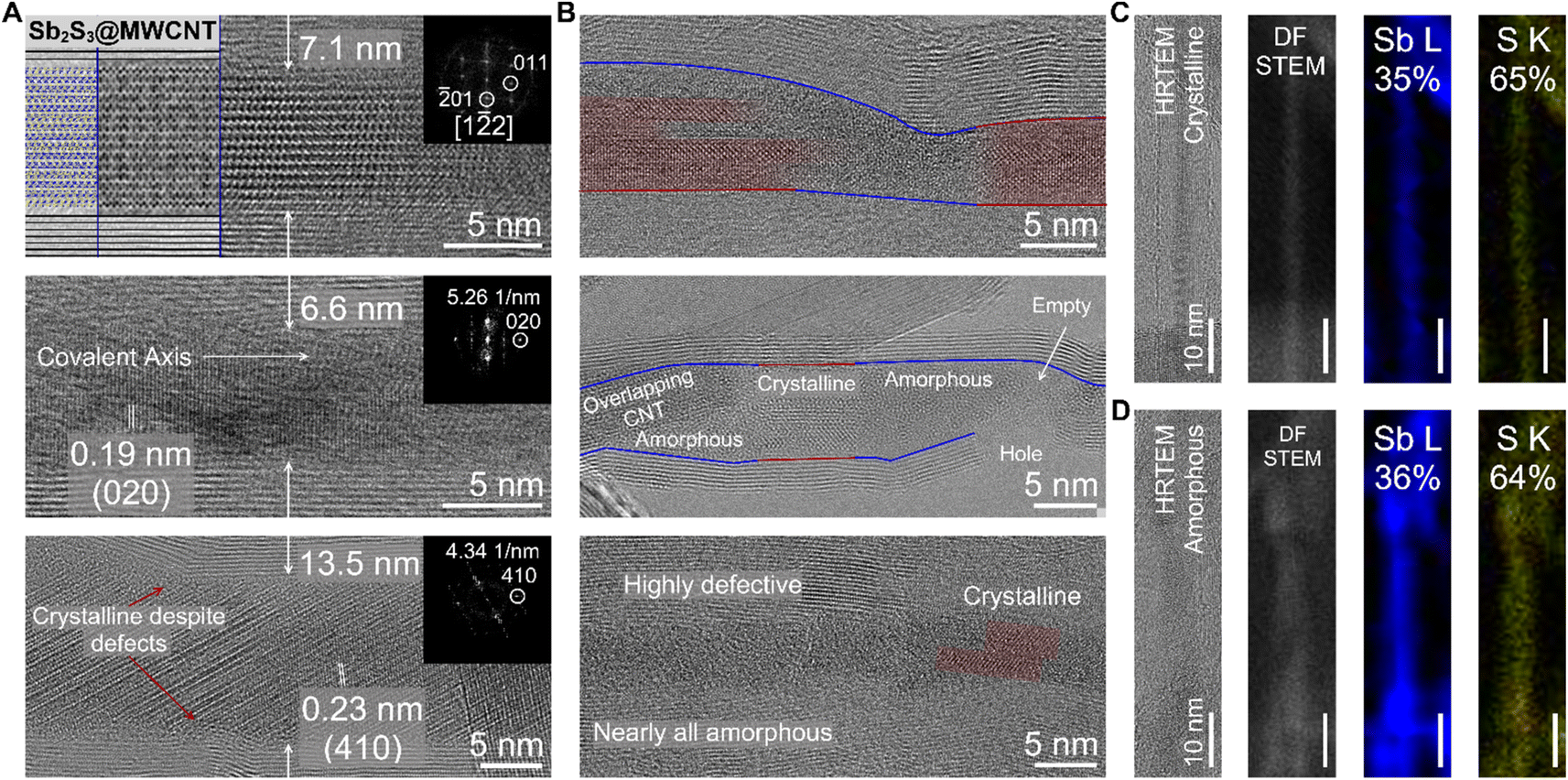 | ||
| Fig. 3 Sb2S3 encapsulated within MWCNTs. (A) Representative HRTEM of crystalline Sb2S3@MWCNTs. The topmost image contains a model (left), simulated image (middle), and real image (right). For all three images, the corresponding FFT of the micrographs are located on the top-right panel. (B) Representative HRTEM of amorphous a-Sb2S3@MWCNTs. The crystalline domains of c-Sb2S3 are highlighted in red for easier visualization, while the a-Sb2S3 domains are highlighted in blue. (C) EDS map of a c-Sb2S3 nanowire bundle encapsulated within a MWCNT. (D) EDS map of an amorphous a-Sb2S3 nanowire within a MWCNT. | ||
To further understand this unusual but reproducible behavior we once again closely examined the possibility that the amorphization is a product of an off-stoichiometric phase with the larger region of interest provided by our MWCNT source (Fig. 3C and D). In a heterostructure where we observe distinct lattice fringes along the length of the wire via HRTEM imaging signifying crystalline order, a corresponding EDS map revealed both Sb and S were present at 35 and 65 atomic percent, respectively, which is close to the stoichiometric ratio of Sb2S3. We attribute the small 5% discrepancy from the true 2:3 Sb/S ratio to instrumental error. While there could have been residual sulfur present on the TEM grid or coating the wires, the EDS map of the S K intensity is exclusively localized to the inner diameter of the nanotubes. Likewise, we also observed a ratio of 36:64 Sb/S for an amorphous phase within the nanotube that we mapped subsequently (on the same grid) which, due to the close agreement of the discrepancy attributable to the measurement error, we are confident the stoichiometric ratio of Sb/S is not the cause of the amorphization of Sb2S3@NTs. This observation further supports the notion that amorphous formation of Sb2S3 within nanotubes is a direct result of the physical effect of the defect on the Sb2S3 rather than the specific chemistry of the host nanotube. We note that nanotubes with large inner diameters retain crystallinity despite the presence of defects (Fig. 3A), signifying that this effect, too, has a nanotube diameter dependence and is likely suppressed by the available free volume for crystallization in larger nanotubes.
Contrastingly, we also observed many Sb2S3 nanowires that were amorphous within the BNNTs despite an apparently smooth nanotube wall making up a majority of the Sb2S3@BNNT sample and sought to understand the rationale for this crystallization behavior (Fig. 4). More specifically, the heterostructures in question appeared to have no noticeable defects or discontinuities along the nanotube walls and showed little to no curvature (Fig. 4A). These nanotubes, for consistency, had diameters that are close to the previously discussed nanotubes. Through these samples, we examined how the more pronounced formation of amorphous domains could be influenced, to some extent, by the difference in interfacial chemistry between CNTs and BNNTs. Electron donation may occur between the CNT and the guest Sb2S3, which may be critical to the stabilization of crystalline c-Sb2S3. DFT analysis of a single Sb2S3 chain projected two-unit-cells long in a (21,0) SWCNT and (21,0) single-walled BNNT (SWBNNT) revealed a significant difference in the host-to-guest electron donation depending on the chemical identity of the nanotube (Fig. 4C). Bader analyses of these simulated structures showed that 0.435 electrons were transferred from the SWCNT to the two-unit-cell-long Sb2S3 in Sb2S3@SWCNT(21,0) while the behavior was reversed and insignificant for the BNNT, with a nominal value of 0.046 electrons transferred from the two-unit-cell-long long Sb2S3 to the BNNT in Sb2S3@SWBNNT(21,0).
 | ||
| Fig. 4 HRTEM of Sb2S3@BNNTs and DFT simulations of Sb2S3@nanotubes. (A) Representative HRTEM image of amorphous a-Sb2S3 domains within apparently smooth and well-defined BNNTs. (B) Representative HRTEM images of BNNTs before filling with Sb2S3. Highlighted in arrows are the BN aggregates that are encapsulated inside the nanotubes. (C) DFT and electron density difference map of crystalline Sb2S3 in a (21,0) SWCNT and (21,0) SWBNNT. | ||
These results are further corroborated by X-ray photoelectron spectroscopy (XPS) of our experimental a-Sb2S3@BNNT and c-Sb2S3@SWCNT samples (Fig. S10 and Table S2†). As observed from our DFT calculations, the dominant electron localization occurs on S rather than Sb in Sb2S3@SWCNT. When we compare the values of the S 2p peaks between c-Sb2S3@SWCNT (2p3/2 = 161.67 eV, 2p1/2 = 162.92 eV, and Δ = 1.25 eV) and a-Sb2S3@BNNT (2p3/2 = 161.95 eV, 2p1/2 = 163.20 eV, and Δ = 1.25 eV) the carbon nanotube has a 0.28 eV lower value, indicating a greater degree of electron density. Meanwhile, the Sb 3d peak values between c-Sb2S3@SWCNT (3d5/2 = 529.95 eV, 3d3/2 = 539.31 eV, and Δ = 9.36 eV) and a-Sb2S3@BNNT (3d5/2 = 529.97 eV, 3d3/2 = 539.4 eV, and Δ = 9.43 eV) are much closer in value and consistent with other Sb2S3 nanowire reports.13 Both @SWCNT and @BNNT Sb and S values are above those of the experimentally determined bulk Sb2S3 values (Sb 3d5/2 = 529.72 eV, 3d3/2 = 539.08 eV, and Δ = 9.36 eV; S 2p3/2 = 161.57 eV, 2p1/2 = 162.81 eV, and Δ = 1.24 eV). While both heterostructures are vdW in nature, this electron reorganization in Sb2S3@SWCNT likely creates a dipole that stabilizes the interaction between guest and host facilitated by carbon's conductivity, while the Sb2S3@SWBNNT system more closely resembles a true vdW interaction. This donation and subsequent weak dipole interaction also has an interesting impact on the thermal stability of the material by thermogravimetric analysis (TGA) (Fig. S11†). While both @NT structures decompose at lower temperatures than the bulk material (632.1 °C) as expected of nanomaterials,77 the c-Sb2S3@SWCNT material (536.6 °C) appears to have a much greater degree of thermal stability compared to the a-Sb2S3@BNNT material (246.9 °C). The fact that the encapsulated Sb2S3 in BNNT is predominantly amorphous could also contribute to this lower thermal stability. Still, despite the appreciable difference in the extent of electron transfer between the readily donating CNT and the relatively inert BNNT, both simulated structures yielded energetically favorable and comparable interactions based on the calculated binding energies (EB) with a resulting EB = −1.83 eV in Sb2S3@SWCNT and EB = −1.52 eV in Sb2S3@BNNT. While the Sb2S3@SWCNT shows a slightly more negative EB and a more energetically favorable interaction, the Sb2S3@BNNT is still energetically favorable, and we find clear examples of c-Sb2S3 nanowires within the BNNTs. From an experimental standpoint, Sb2S3 nanowires can also readily crystallize outside of a nanotube which means that ultrathin Sb2S3 is not a metastable phase.13 As such, based on these arguments, we posit that as electron donation from the carbon nanotubes stabilizes the Sb2S3 chain, the lack of donation from BNNTs does not destabilize the chain.
To complement these observations, we also experimentally evaluated the quality of the empty BNNT precursors that we used for filling and found obvious aggregates of BN already inside most of the tubes (Fig. 4B). These aggregates, along with other inner tube wall defects and discontinuities, are present at the time of nanotube synthesis and were not removed unlike other BN impurities. From our imaging studies, we found that the aggregates persisted after calcining the BNNTs at 800 °C in open air for 5 hours and even after washing in aqua regia for 5 h followed by calcination (Fig. S12†). Observations from other literature reports that utilized the same nanotube source also observed the same aggregates encapsulated within the nanotubes resulting from the aggressive post-synthesis treatment to open the ends.78 These observations suggest that these aggregates likely act in the same way nanotube wall defects do, disrupting crystal packing and causing the amorphous phase to be preferred. In line with our prior discussion, we further reason that this is the likely cause for the formation of amorphous domains for the large majority of the Sb2S3 within the BNNTs despite the BNNT walls being predominantly smooth, rather than the lack of electron donation from the host nanotube to the guest Sb2S3 structure.
From HRTEM imaging coupled with EDS mapping, we have corroborated that the degree of crystallinity found in Sb2S3@NTs is strongly dependent on the crystalline order and quality of material it interfaces with. In smooth and continuous nanotubes, we consistently observed c-Sb2S3. In contrast, in jagged or narrowing nanotubes, we found a-Sb2S3 domains especially at narrow (<10 nm) nanotube diameters. We surmise that this difference can be rationalized in terms of the interfacial stability between the Sb2S3 phase and the host nanotube. As a unique 1D PCM, the literature has established that the energy difference between the c-Sb2S3 and a-Sb2S3 phases is low.79 Owing to its crystalline and highly anisotropic nature, the growth of c-Sb2S3 has the geometric propensity to adopt a 1D nanostructure as imposed by its [Sb4S6]n chain building blocks. Against an atomically rough or discontinuous nanotube surface, however, a propagating chain and bundle of c-Sb2S3 will require more free space within the nanotube (and along the direction of the chain propagation) to consistently crystallize linearly as 1D crystals and will be limited by the distance of the furthest extended defect of the nanotube wall. Hence, while the c-Sb2S3 may be slightly more energetically favorable than the amorphous phase outside the nanotube, the presence of defects along the nanotube inner walls could destabilize the favorable interfacial vdW interaction between the encapsulated Sb2S3 phase and the nanotube host. In contrast, a-Sb2S3 can readily solidify to occupy any geometric configuration and shape of the host nanotube. This structural modularity of an amorphous phase means it can readily fill the irregular void space that would destabilize the c-Sb2S3 phase, thereby maximizing the surface stability of the a-Sb2S3@NT heterointerface.
We note that the amorphous phase is not limited to the areas immediately surrounding the defect and, instead, appears to saturate a sizable nanotube region several nanometers beyond the nanotube defect (Fig. 2C and 3B). From these results, we posit that thermodynamic surface stability of the amorphous phase at the interface drives the immediate surrounding nanotube area to favor the formation of amorphous domains, diminishing the crystalline phase except in very smooth regions where the c-Sb2S3 phase preferentially forms. Our observation of the diameter dependence of this effect, wherein defects do not strictly cause amorphous phases or domains at large diameters (>10 nm), suggests a competition between Ostwald ripening80 and the recently discovered defect-mediated ripening.81 The former involves a large crystalline domain within the nanotube that drives the system toward a crystalline phase regardless of defects while the latter involves the higher intrinsic interfacial stability of an amorphous phase within the nanotube that drives the system towards that the formation of amorphous domains at the vicinity of defect sites along the nanotube walls. In terms of growth, this would imply that the liquid Sb2S3 melt migrates into the nanotubes at high temperatures. Then, as the reaction cools, the Sb2S3 melt solidifies in a way that minimizes its surface energy: either by directionally crystallizing in small, defect-free nanotubes in the direction parallel to the long axis of the nanotube or by condensing as an amorphous solid to occupy the defective regions. At larger nanotube diameters, we observe that both mechanisms break down, resulting in decreased directionality in the crystallization and crystalline quality regardless of defects as the stability of a “bulk” crystal becomes more pronounced than that of the interface. We do not see any significant difference between CNTs and BNNTs in this regard, as even though CNTs have a more stable interface with c-Sb2S3 based on our calculations, we still find a-Sb2S3 at CNT wall defects. Structural selectivity has been reported previously, in which nanotube diameter dictates the phase of the guest,82,83 though amorphous phases at defects and diameter-dependent control over covalent direction have not. We note that this result is not unique to 1D systems but is also consistent with literature reports in comparable 2D synthetic platforms, in which the formation of thin film domains of a-Sb2S3 templated onto a graphene substrate is greatly facilitated by ozone-induced defects in the surface.25
Our understanding of the formation of a-Sb2S3 and c-Sb2S3 domains in BNNTs has provided an opportunity to evaluate the optoelectronic properties of confined amorphous domains of Sb2S3 encapsulated within an optically transparent (in the visible range) and electrically insulating BNNTs. These Sb2S3@BNNT heterostructures are predominantly comprised of a-Sb2S3@BNNTs with some c-Sb2S3@BNNTs (Fig. 5). From the sample under study, the consequences of encapsulation were immediately obvious from the red-orange appearance (in contrast with the empty BNNTs that are white) of the a-Sb2S3@BNNT ensemble collected from the mixed melt synthesis product (Fig. 5A). In our efforts to quantify the absorbance of the a-Sb2S3@BNNT, we found that estimating the Kubelka–Munk absorbance from DRS was inconsistent, as empty BNNTs reflected more of the incident light than the KBr used for the sample matrix and the blank measurement. Instead, we used UV-vis spectroscopy to probe the absorption signatures of a-Sb2S3@BNNTs suspended in isopropanol (Fig. 5B). The resulting spectrum showed an obvious absorption edge that emerged at ∼502 nm/2.47 eV. This is in the high energy end of the typical 1.7–2.8 eV absorption range of a-Sb2S3 as found in the literature25,27,30 and is a significant 0.89 eV blue shift from the 790 nm/1.57 eV band gap absorption edge of bulk crystalline Sb2S3. Meanwhile, the Raman spectrum of a-Sb2S3@BNNT matches literature reports of a-Sb2S3,31 with only one broad peak centered around 300 cm−1. This broad peak corresponding to the amorphous phase does not display a shoulder peak unlike the Raman peak apparent in our c-Sb2S3@CNTs, corroborating our observations made by HRTEM that most of the material is a-Sb2S3 within the BNNTs (Fig. 5C). While amorphous, these results still demonstrate that BNNTs can be sensitized using an inorganic guest (amorphous or crystalline) to absorb well within the visible range.
 | ||
| Fig. 5 Optoelectronic properties of primarily a-Sb2S3 encapsulated within BNNTs. (A) Optical images of a-Sb2S3@BNNTs (left) and BNNTs (right). (B) UV-vis spectra of a-Sb2S3@BNNTs and BNNTs overlayed with DRS of crystalline Sb2S3. (C) Raman spectra of a-Sb2S3@BNNTs, crystalline Sb2S3, and BNNTs. (D) Device schematic of pressed pellet of a-Sb2S3@BNNTs. (E) Photocurrent response of pressed pellet of purified a-Sb2S3@BNNTs illuminated with a 13 mW cm−2 light source. | ||
Finally, we demonstrate that filling BNNTs with mostly a-Sb2S3 also imparts a degree of electrical conductivity to the heterostructure when pressed as ensemble pellets (Fig. 5D and E). To fabricate devices from filled and empty BNNTs, we pelletized each at 14 MPa then fabricated roughly uniform rectangular sections from the resulting pellet. Comparative measurements for both filled and empty BNNTs were made using identical contacts (indium metal) and device geometry (two-probe contacts), with dimensions that were measured and accounted for. The devices were then illuminated by a pulsed 415 nm LED light at 13 mW (Fig. 5D). From the current vs. time plot, we observed a well-resolved and prominent photocurrent response for the a-Sb2S3@BNNT device but not for the empty BNNT device (Fig. 5E). This indicates any measurable photocurrent arises from the a-Sb2S3 nanostructures encapsulated inside of the nanotubes. We also observed an uptick in conductivity, from 5.1 nS cm−1 in empty BNNTs to 8.3 nS cm−1 in a-Sb2S3@BNNTs (Fig. S13†). These results suggest that pronounced alterations in the optical, electrical, and optoelectronic behavior of composite BNNT-encapsulated 1D or quasi-1D vdW crystals can be realized even with amorphous encapsulated domains. From these results, we envision that the dispersibility of the Sb2S3@BNNT assembly and the stability of the ultranarrow heterostructures indicates that significant improvements can be made via more optimized device fabrication to improve the active building blocks and create effective single wire photoresistors of only a few nm in width. The insulating nature of the BNNT means the conduction is strongly influenced by the Sb2S3 guest which could potentially serve as ultranarrow semiconductor building blocks for next-generation transistor platforms.70 Finally, BN-semiconductor heterostructures have demonstrated good capability as thermoelectric devices in 2D,84 and this class of heterostructure could also serve as a 1D platform for waste heat recovery and thermoelectric power generation.
3 Conclusion
In this report, we demonstrated that single- and multi-walled carbon and boron nitride nanotube encapsulation can be used to control the size, growth direction/orientation, and degree of crystallinity of Sb2S3, a model quasi-1D vdW crystal, from nanowire bundles down to the single chain regime. We establish that using highly uniform SWCNTs facilitates the formation of continuous few-chain nanowires and single covalent chains, directing growth strictly to the [010]-direction. On the contrary, we systematically observed that using either BNNTs or MWCNTs with inner wall defects led to the formation of a-Sb2S3 domains localized around the defects. We observed that this effect was nanotube size-/diameter-dependent, with larger nanotubes crystallizing encapsulated Sb2S3 nanostructures regardless of defects in the tube wall in addition to diminished control over the growth orientation. Beyond our understanding of the possible growth and crystallization pathways of Sb2S3, our ability to synthesize ensembles of Sb2S3@nanotube heterostructures with a visible light-transparent and insulating BNNT also enabled us to evaluate the unobscured optical and electrical properties of ultrathin, predominantly amorphous, Sb2S3 few-chain nanowire bundles. Altogether, our study on the synthetic modulation of Sb2S3 nanostructures, either crystalline or amorphous and at or approaching the single chain regime, underscores the critical role of the host–guest interface on the formation of well-defined structural domains, the spectrum of accessible optical and electronic states, and the prospects of encapsulated quasi-1D vdW guest nanomaterials with applications in energy conversion such as photovoltaics and thermoelectric generation as well as in computing and data storage devices.Data availability
All data are available in the main text or the ESI.†Author contributions
G. M. M.: methodology, investigation, visualization, and writing – original draft preparation; D. L. M. C.: methodology, investigation, and writing – reviewing and editing; Z. Y.: methodology, investigation, and writing – reviewing and editing; B. Y. Z.: investigation; L. R. S.: methodology, investigation; T. A.: methodology, investigation; M. Q. A.: conceptualization, supervision, and writing – reviewing and editing.Conflicts of interest
The authors have no conflicts of interest to declare.Acknowledgements
This work was supported by the National Science Foundation under Award No. DMR-2340918. G. M. M. is funded by the National Science Foundation (2023331840) through the NSF Graduate Research Fellowships Program. Several aspects of this work were performed at the UC Irvine Materials Research Institute (IMRI). Facilities and instrumentation at IMRI are supported, in part, by the National Science Foundation through the UC Irvine Materials Research Science and Engineering Center grant number DMR-2011967. XPS work was performed using instruments funded, in part, by the National Science Foundation Major Research Instrumentation Program (CHE-1338173).References
- M. Zeng, Y. Xiao, J. Liu, K. Yang and L. Fu, Exploring Two-Dimensional Materials toward the Next-Generation Circuits: From Monomer Design to Assembly Control, Chem. Rev., 2018, 118(13), 6236–6296, DOI:10.1021/acs.chemrev.7b00633.
- Y. Lei, T. Zhang, Y.-C. Lin, T. Granzier-Nakajima, G. Bepete, D. A. Kowalczyk, Z. Lin, D. Zhou, T. F. Schranghamer, A. Dodda, A. Sebastian, Y. Chen, Y. Liu, G. Pourtois, T. J. Kempa, B. Schuler, M. T. Edmonds, S. Y. Quek, U. Wurstbauer, S. M. Wu, N. R. Glavin, S. Das, S. P. Dash, J. M. Redwing, J. A. Robinson and M. Terrones, Graphene and Beyond: Recent Advances in Two-Dimensional Materials Synthesis, Properties, and Devices, ACS Nanosci. Au, 2022, 2(6), 450–485, DOI:10.1021/acsnanoscienceau.2c00017.
- V. Shanmugam, R. A. Mensah, K. Babu, S. Gawusu, A. Chanda, Y. Tu, R. E. Neisiany, M. Försth, G. Sas and O. Das, A Review of the Synthesis, Properties, and Applications of 2D Materials, Part. Part. Syst. Charact., 2022, 39(6), 2200031, DOI:10.1002/ppsc.202200031.
- A. A. Balandin, F. Kargar, T. T. Salguero and R. K. Lake, One-Dimensional van Der Waals Quantum Materials, Mater. Today, 2022, 55, 74–91, DOI:10.1016/j.mattod.2022.03.015.
- A. A. Balandin, R. K. Lake and T. T. Salguero, One-Dimensional van Der Waals Materials—Advent of a New Research Field, Appl. Phys. Lett., 2022, 121(4), 040401, DOI:10.1063/5.0108414.
- J. N. Coleman, M. Lotya, A. O'Neill, S. D. Bergin, P. J. King, U. Khan, K. Young, A. Gaucher, S. De, R. J. Smith, I. V. Shvets, S. K. Arora, G. Stanton, H.-Y. Kim, K. Lee, G. T. Kim, G. S. Duesberg, T. Hallam, J. J. Boland, J. J. Wang, J. F. Donegan, J. C. Grunlan, G. Moriarty, A. Shmeliov, R. J. Nicholls, J. M. Perkins, E. M. Grieveson, K. Theuwissen, D. W. McComb, P. D. Nellist and V. Nicolosi, Two-Dimensional Nanosheets Produced by Liquid Exfoliation of Layered Materials, Science, 2011, 331(6017), 568–571, DOI:10.1126/science.1194975.
- Z. Wang, X. Yan, Q. Hou, Y. Liu, X. Zeng, Y. Kang, W. Zhao, X. Li, S. Yuan, R. Qiu, M. H. Uddin, R. Wang, Y. Xia, M. Jian, Y. Kang, L. Gao, S. Liang, J. Z. Liu, H. Wang and X. Zhang, Scalable High Yield Exfoliation for Monolayer Nanosheets, Nat. Commun., 2023, 14(1), 236, DOI:10.1038/s41467-022-35569-8.
- X. Qian, Y. Wang, Z. Ju, M. Xie, B. Zhang and G. Yu, Chemical Exfoliation of Metal Oxide Nanosheets for High-Performance Ion Conducting Membranes, ACS Mater. Lett., 2022, 4(11), 2321–2327, DOI:10.1021/acsmaterialslett.2c00843.
- Y. Sozen, J. J. Riquelme, Y. Xie, C. Munuera and A. Castellanos-Gomez, High-Throughput Mechanical Exfoliation for Low-Cost Production of van Der Waals Nanosheets, Small Methods, 2023, 7(10), 2300326, DOI:10.1002/smtd.202300326.
- J. S. Lee, S. Brittman, D. Yu and H. Park, Vapor–Liquid–Solid and Vapor–Solid Growth of Phase-Change Sb2Te3 Nanowires and Sb2Te3/GeTe Nanowire Heterostructures, J. Am. Chem. Soc., 2008, 130(19), 6252–6258, DOI:10.1021/ja711481b.
- D. Zhou, H. Shu, C. Hu, L. Jiang, P. Liang and X. Chen, Unveiling the Growth Mechanism of MoS2 with Chemical Vapor Deposition: From Two-Dimensional Planar Nucleation to Self-Seeding Nucleation, Cryst. Growth Des., 2018, 18(2), 1012–1019, DOI:10.1021/acs.cgd.7b01486.
- S. H. Lee, B. Lee, B. J. Kim, B. J. Jeong, S. Cho, H. E. Jang, H. H. Cho, J.-H. Lee, J.-H. Park, H. K. Yu and J.-Y. Choi, Liquid Precursor-Assisted Chemical Vapor Deposition of One-Dimensional van Der Waals Material Nb2Se9: Tunable Growth for Room-Temperature Gas Sensors, ACS Sens., 2022, 7(7), 1912–1918, DOI:10.1021/acssensors.2c00512.
- D. L. M. Cordova, K. Chua, R. M. Huynh, T. Aoki and M. Q. Arguilla, Anisotropy-Driven Crystallization of Dimensionally Resolved Quasi-1D Van Der Waals Nanostructures, J. Am. Chem. Soc., 2023, 145(41), 22413–22424, DOI:10.1021/jacs.3c05887.
- K. F. Mak, C. Lee, J. Hone, J. Shan and T. F. Heinz, Atomically Thin MoS2: A New Direct-Gap Semiconductor, Phys. Rev. Lett., 2010, 105(13), 136805, DOI:10.1103/PhysRevLett.105.136805.
- C. L. Kane and E. J. Mele, Quantum Spin Hall Effect in Graphene, Phys. Rev. Lett., 2005, 95(22), 226801, DOI:10.1103/PhysRevLett.95.226801.
- Y. J. Zhang, T. Ideue, M. Onga, F. Qin, R. Suzuki, A. Zak, R. Tenne, J. H. Smet and Y. Iwasa, Enhanced Intrinsic Photovoltaic Effect in Tungsten Disulfide Nanotubes, Nature, 2019, 570(7761), 349–353, DOI:10.1038/s41586-019-1303-3.
- Y. Qu, M. Q. Arguilla, Q. Zhang, X. He and M. Dincă, Ultrathin, High-Aspect Ratio, and Free-Standing Magnetic Nanowires by Exfoliation of Ferromagnetic Quasi-One-Dimensional van Der Waals Lattices, J. Am. Chem. Soc., 2021, 143(46), 19551–19558, DOI:10.1021/jacs.1c09607.
- T. A. Empante, A. Martinez, M. Wurch, Y. Zhu, A. K. Geremew, K. Yamaguchi, M. Isarraraz, S. Rumyantsev, E. J. Reed, A. A. Balandin and L. Bartels, Low Resistivity and High Breakdown Current Density of 10 Nm Diameter van Der Waals TaSe3 Nanowires by Chemical Vapor Deposition, Nano Lett., 2019, 19(7), 4355–4361, DOI:10.1021/acs.nanolett.9b00958.
- S. Ghosh, F. Kargar, N. R. Sesing, Z. Barani, T. T. Salguero, D. Yan, S. Rumyantsev and A. A. Balandin, Low-Frequency Current Fluctuations in Quasi-1D (TaSe4)2I Weyl Semimetal Nanoribbons, Adv. Electron. Mater., 2023, 9(2), 2200860, DOI:10.1002/aelm.202200860.
- P. Bayliss and W. Nowacki, Refinement of the crystal structure of stibnite, Sb2S3, Z. Fur Krist. – Cryst. Mater., 1972, 135(1–6), 308–315, DOI:10.1524/zkri.1972.135.16.308.
- Stibnite, Handbook of Mineralogy, Mineralogical Society of America, USA, 2023 Search PubMed.
- Metastibnite, Handbook of Mineralogy, Mineralogical Society of America, USA, 2023 Search PubMed.
- U. A. Shah, S. Chen, G. M. G. Khalaf, Z. Jin and H. Song, Wide Bandgap Sb2S3 Solar Cells, Adv. Funct. Mater., 2021, 31(27), 2100265, DOI:10.1002/adfm.202100265.
- H. Maghraoui-Meherzi, T. Ben Nasr, N. Kamoun and M. Dachraoui, Structural, Morphology and Optical Properties of Chemically Deposited Sb2S3 Thin Films, Phys. B Condens. Matter, 2010, 405(15), 3101–3105, DOI:10.1016/j.physb.2010.04.020.
- J.-H. Chen, S.-K. Chiu, J.-D. Luo, S.-Y. Huang, H.-A. Ting, M. Hofmann, Y.-P. Hsieh and C.-C. Ting, Robust Formation of Amorphous Sb2S3 on Functionalized Graphene for High-Performance Optoelectronic Devices in the Cyan-Gap, Sci. Rep., 2020, 10(1), 14873, DOI:10.1038/s41598-020-70879-1.
- Z. Cui, K. Bu, Y. Zhuang, M.-E. Donnelly, D. Zhang, P. Dalladay-Simpson, R. T. Howie, J. Zhang, X. Lü and Q. Hu, Phase Transition Mechanism and Bandgap Engineering of Sb2S3 at Gigapascal Pressures, Commun. Chem., 2021, 4(1), 1–8, DOI:10.1038/s42004-021-00565-4.
- S.-J. Lee, S.-J. Sung, K.-J. Yang, J.-K. Kang, J. Y. Kim, Y. S. Do and D.-H. Kim, Approach to Transparent Photovoltaics Based on Wide Band Gap Sb2S3 Absorber Layers and Optics-Based Device Optimization, ACS Appl. Energy Mater., 2020, 3(12), 12644–12651, DOI:10.1021/acsaem.0c02552.
- Q. Wang, Z. Chen, J. Wang, Y. Xu, Y. Wei, Y. Wei, L. Qiu, H. Lu, Y. Ding and J. Zhu, Sb2S3 Solar Cells: Functional Layer Preparation and Device Performance, Inorg. Chem. Front., 2019, 6(12), 3381–3397, 10.1039/C9QI00800D.
- A. D. Vos, Detailed Balance Limit of the Efficiency of Tandem Solar Cells, J. Phys. Appl. Phys., 1980, 13(5), 839, DOI:10.1088/0022-3727/13/5/018.
- C. Ghosh and B. P. Varma, Optical Properties of Amorphous and Crystalline Sb2S3 Thin Films, Thin Solid Films, 1979, 60(1), 61–65, DOI:10.1016/0040-6090(79)90347-X.
- M. Delaney, I. Zeimpekis, D. Lawson, D. W. Hewak and O. L. Muskens, A New Family of Ultralow Loss Reversible Phase-Change Materials for Photonic Integrated Circuits: Sb2S3 and Sb2Se3, Adv. Funct. Mater., 2020, 30(36), 2002447, DOI:10.1002/adfm.202002447.
- M. Wuttig and S. Raoux, The Science and Technology of Phase Change Materials, Z. Anorg. Allg. Chem., 2012, 638(15), 2455–2465, DOI:10.1002/zaac.201200448.
- P. Noé, C. Vallée, F. Hippert, F. Fillot and J.-Y. Raty, Phase-Change Materials for Non-Volatile Memory Devices: From Technological Challenges to Materials Science Issues, Semicond. Sci. Technol., 2017, 33(1), 013002, DOI:10.1088/1361-6641/aa7c25.
- S. Raoux, C. T. Rettner, J. L. Jordan-Sweet, A. J. Kellock, T. Topuria, P. M. Rice and D. C. Miller, Direct Observation of Amorphous to Crystalline Phase Transitions in Nanoparticle Arrays of Phase Change Materials, J. Appl. Phys., 2007, 102(9), 094305, DOI:10.1063/1.2801000.
- R. Golovchak, J. Plummer, A. Kovalskiy, Y. Holovchak, T. Ignatova, K. Nowlin, A. Trofe, Y. Shpotyuk, C. Boussard-Pledel and B. Bureau, Broadband Photosensitive Medium Based on Amorphous Equichalcogenides, ACS Appl. Electron. Mater., 2022, 4(11), 5397–5405, DOI:10.1021/acsaelm.2c01075.
- R. Golovchak, J. Plummer, A. Kovalskiy, Y. Holovchak, T. Ignatova, A. Trofe, B. Mahlovanyi, J. Cebulski, P. Krzeminski, Y. Shpotyuk, C. Boussard-Pledel and B. Bureau, Phase-Change Materials Based on Amorphous Equichalcogenides, Sci. Rep., 2023, 13(1), 2881, DOI:10.1038/s41598-023-30160-7.
- X. Wang, Z. Li, S. R. Kavanagh, A. M. Ganose and A. Walsh, Lone Pair Driven Anisotropy in Antimony Chalcogenide Semiconductors, Phys. Chem. Chem. Phys., 2022, 24(12), 7195–7202, 10.1039/D1CP05373F.
- J. Li, Y. Niu, J. Zeng, J. Wang, Q. Wang, X. Liu, H. Li, N. F. de Rooij, Y. Wang and G. Zhou, Electrochemical Exfoliation of Naturally Occurring Layered Mineral Stibnite (Sb2S3) for Highly Sensitive and Fast Room-Temperature Acetone Sensing, Adv. Mater. Interfaces, 2022, 9(19), 2200605, DOI:10.1002/admi.202200605.
- S. M. Tan, C. C. Mayorga-Martinez, Z. Sofer and M. Pumera, Bipolar Electrochemistry Exfoliation of Layered Metal Chalcogenides Sb2S3 and Bi2S3 and Their Hydrogen Evolution Applications, Chem.–Eur. J., 2020, 26(29), 6479–6483, DOI:10.1002/chem.201904767.
- F. Caruso, M. R. Filip and F. Giustino, Excitons in One-Dimensional van Der Waals Materials: Sb2S3 Nanoribbons, Phys. Rev. B: Condens. Matter Mater. Phys., 2015, 92(12), 125134, DOI:10.1103/PhysRevB.92.125134.
- R. Malakooti, L. Cademartiri, A. Migliori and G. A. Ozin, Ultrathin Sb2S3 nanowires and Nanoplatelets, J. Mater. Chem., 2007, 18(1), 66–69, 10.1039/B713383A.
- J. Yang, Y.-C. Liu, H.-M. Lin and C.-C. Chen, A Chain-Structure Nanotube: Growth and Characterization of Single-Crystal Sb2S3 Nanotubes via a Chemical Vapor Transport Reaction, Adv. Mater., 2004, 16(8), 713–716, DOI:10.1002/adma.200305757.
- K. Ye, B. Wang, A. Nie, K. Zhai, F. Wen, C. Mu, Z. Zhao, J. Xiang, Y. Tian and Z. Liu, Broadband Photodetector of High Quality Sb2S3 Nanowire Grown by Chemical Vapor Deposition, J. Mater. Sci. Technol., 2021, 75, 14–20, DOI:10.1016/j.jmst.2020.10.005.
- J. Guo, R. Xiang, T. Cheng, S. Maruyama and Y. Li, One-Dimensional van Der Waals Heterostructures: A Perspective, ACS Nanosci. Au, 2022, 2(1), 3–11, DOI:10.1021/acsnanoscienceau.1c00023.
- M. Monthioux, Carbon Meta-Nanotubes: Synthesis, Properties and Applications, Wiley, USA, 2011 Search PubMed.
- T. Pham, S. Oh, P. Stetz, S. Onishi, C. Kisielowski, M. L. Cohen and A. Zettl, Torsional Instability in the Single-Chain Limit of a Transition Metal Trichalcogenide, Science, 2018, 361(6399), 263–266, DOI:10.1126/science.aat4749.
- C. A. Slade, A. M. Sanchez and J. Sloan, Unprecedented New Crystalline Forms of SnSe in Narrow to Medium Diameter Carbon Nanotubes, Nano Lett., 2019, 19(5), 2979–2984, DOI:10.1021/acs.nanolett.9b00133.
- A. Vasylenko, S. Marks, J. M. Wynn, P. V. C. Medeiros, Q. M. Ramasse, A. J. Morris, J. Sloan and D. Quigley, Electronic Structure Control of Sub-Nanometer 1D SnTe via Nanostructuring within Single-Walled Carbon Nanotubes, ACS Nano, 2018, 12(6), 6023–6031, DOI:10.1021/acsnano.8b02261.
- A. A. Eliseev, N. S. Falaleev, N. I. Verbitskiy, A. A. Volykhov, L. V. Yashina, A. S. Kumskov, V. G. Zhigalina, A. L. Vasiliev, A. V. Lukashin, J. Sloan and N. A. Kiselev, Size-Dependent Structure Relations between Nanotubes and Encapsulated Nanocrystals, Nano Lett., 2017, 17(2), 805–810, DOI:10.1021/acs.nanolett.6b04031.
- R. J. Kashtiban, C. E. Patrick, Q. Ramasse, R. I. Walton and J. Sloan, Picoperovskites: The Smallest Conceivable Isolated Halide Perovskite Structures Formed within Carbon Nanotubes, Adv. Mater., 2023, 35(10), 2208575, DOI:10.1002/adma.202208575.
- M. Gao, Y. Park, J. Jin, P.-C. Chen, H. Devyldere, Y. Yang, C. Song, Z. Lin, Q. Zhao, M. Siron, M. C. Scott, D. T. Limmer and P. Yang, Direct Observation of Transient Structural Dynamics of Atomically Thin Halide Perovskite Nanowires, J. Am. Chem. Soc., 2023, 145(8), 4800–4807, DOI:10.1021/jacs.2c13711.
- R. Saito, M. Fujita, G. Dresselhaus and M. S. Dresselhaus, Electronic Structure of Chiral Graphene Tubules, Appl. Phys. Lett., 1992, 60(18), 2204–2206, DOI:10.1063/1.107080.
- Y. Matsuda, J. Tahir-Kheli and W. A. I. Goddard, Definitive Band Gaps for Single-Wall Carbon Nanotubes, J. Phys. Chem. Lett., 2010, 1(19), 2946–2950, DOI:10.1021/jz100889u.
- V. Ghai, H. Singh and P. K. Agnihotri, Structure Dependent Broadband Optical Absorption in Carbon Nanotubes, ACS Appl. Opt. Mater., 2023, 1(1), 252–260, DOI:10.1021/acsaom.2c00047.
- W. Cheung, M. Patel, Y. Ma, Y. Chen, Q. Xie, J. V. Lockard, Y. Gao and H. He, π-Plasmon Absorption of Carbon Nanotubes for the Selective and Sensitive Detection of Fe3+ Ions, Chem. Sci., 2016, 7(8), 5192–5199, 10.1039/C6SC00006A.
- D. Wickramaratne, L. Weston and C. G. Van de Walle, Monolayer to Bulk Properties of Hexagonal Boron Nitride, J. Phys. Chem. C, 2018, 122(44), 25524–25529, DOI:10.1021/acs.jpcc.8b09087.
- L. Museur and A. Kanaev, Near Band-Gap Electronics Properties and Luminescence Mechanisms of Boron Nitride Nanotubes, J. Appl. Phys., 2015, 118(8), 084305, DOI:10.1063/1.4928835.
- C. Elias, P. Valvin, T. Pelini, A. Summerfield, C. J. Mellor, T. S. Cheng, L. Eaves, C. T. Foxon, P. H. Beton, S. V. Novikov, B. Gil and G. Cassabois, Direct Band-Gap Crossover in Epitaxial Monolayer Boron Nitride, Nat. Commun., 2019, 10(1), 2639, DOI:10.1038/s41467-019-10610-5.
- G. Cassabois, P. Valvin and B. Gil, Hexagonal Boron Nitride Is an Indirect Bandgap Semiconductor, Nat. Photonics, 2016, 10(4), 262–266, DOI:10.1038/nphoton.2015.277.
- N. G. Chopra, R. J. Luyken, K. Cherrey, V. H. Crespi, M. L. Cohen, S. G. Louie and A. Zettl, Boron Nitride Nanotubes, Science, 1995, 269(5226), 966–967, DOI:10.1126/science.269.5226.966.
- J. W. Jordan, A. I. Chernov, G. A. Rance, E. Stephen Davies, A. E. Lanterna, J. Alves Fernandes, A. Grüneis, Q. Ramasse, G. N. Newton and A. N. Khlobystov, Host–Guest Chemistry in Boron Nitride Nanotubes: Interactions with Polyoxometalates and Mechanism of Encapsulation, J. Am. Chem. Soc., 2023, 145(2), 1206–1215, DOI:10.1021/jacs.2c10961.
- C. Allard, L. Schué, F. Fossard, G. Recher, R. Nascimento, E. Flahaut, A. Loiseau, P. Desjardins, R. Martel and E. Gaufrès, Confinement of Dyes inside Boron Nitride Nanotubes: Photostable and Shifted Fluorescence down to the Near Infrared, Adv. Mater., 2020, 32(29), 2001429, DOI:10.1002/adma.202001429.
- A. Badon, J.-B. Marceau, C. Allard, F. Fossard, A. Loiseau, L. Cognet, E. Flahaut, G. Recher, N. Izard, R. Martel and E. Gaufrès, Fluorescence Anisotropy Using Highly Polarized Emitting Dyes Confined inside BNNTs, Mater. Horiz., 2023, 10(3), 983–992, 10.1039/D2MH01239A.
- T. Pham, A. Fathalizadeh, B. Shevitski, S. Turner, S. Aloni and A. Zettl, A Universal Wet-Chemistry Route to Metal Filling of Boron Nitride Nanotubes, Nano Lett., 2016, 16(1), 320–325, DOI:10.1021/acs.nanolett.5b03874.
- Y. Bando, K. Ogawa and D. Golberg, Insulating `nanocables': Invar Fe–Ni Alloy Nanorods inside BN Nanotubes, Chem. Phys. Lett., 2001, 347(4), 349–354, DOI:10.1016/S0009-2614(01)01075-2.
- F.-F. Xu, Y. Bando, D. Golberg, M. Hasegawa and M. Mitome, Phases and Crystallization of Encapsulated Cobalt Nanorods inside BN Nanotubes, Acta Mater., 2004, 52(3), 601–606, DOI:10.1016/j.actamat.2003.09.043.
- D. Golberg, F.-F. Xu and Y. Bando, Filling Boron Nitride Nanotubes with Metals, Appl. Phys. A, 2003, 76(4), 479–485, DOI:10.1007/s00339-002-2041-0.
- D. Datz, G. Németh, K. E. Walker, G. A. Rance, Á. Pekker, A. N. Khlobystov and K. Kamarás, Polaritonic Enhancement of Near-Field Scattering of Small Molecules Encapsulated in Boron Nitride Nanotubes: Chemical Reactions in Confined Spaces, ACS Appl. Nano Mater., 2021, 4(5), 4335–4339, DOI:10.1021/acsanm.1c00064.
- K. E. Walker, G. A. Rance, Á. Pekker, H. M. Tóháti, M. W. Fay, R. W. Lodge, C. T. Stoppiello, K. Kamarás and A. N. Khlobystov, Growth of Carbon Nanotubes inside Boron Nitride Nanotubes by Coalescence of Fullerenes: Toward the World's Smallest Coaxial Cable, Small Methods, 2017, 1(9), 1700184, DOI:10.1002/smtd.201700184.
- J.-K. Qin, P.-Y. Liao, M. Si, S. Gao, G. Qiu, J. Jian, Q. Wang, S.-Q. Zhang, S. Huang, A. Charnas, Y. Wang, M. J. Kim, W. Wu, X. Xu, H.-Y. Wang, L. Yang, Y. Khin Yap and P. D. Ye, Raman Response and Transport Properties of Tellurium Atomic Chains Encapsulated in Nanotubes, Nat. Electron., 2020, 3(3), 141–147, DOI:10.1038/s41928-020-0365-4.
- W.-Q. Han, C. W. Chang and A. Zettl, Encapsulation of One-Dimensional Potassium Halide Crystals within BN Nanotubes, Nano Lett., 2004, 4(7), 1355–1357, DOI:10.1021/nl0494452.
- G. M. Milligan, D. L. M. Cordova, Z. F. Yao, B. Tong and M. Q. Arguilla, Single Quasi-1D Chains of Sb2Se3 Encapsulated Within Carbon Nanotubes, Chem. Mater., 2024, 36(2), 730–741, DOI:10.1021/acs.chemmater.3c02114.
- I. Efthimiopoulos, C. Buchan and Y. Wang, Structural Properties of Sb2S3 under Pressure: Evidence of an Electronic Topological Transition, Sci. Rep., 2016, 6(1), 24246, DOI:10.1038/srep24246.
- M. S. Dresselhaus, A. Jorio, M. Hofmann, G. Dresselhaus and R. Saito, Perspectives on Carbon Nanotubes and Graphene Raman Spectroscopy, Nano Lett., 2010, 10(3), 751–758, DOI:10.1021/nl904286r.
- M. S. Dresselhaus, G. Dresselhaus, R. Saito and A. Jorio, Raman Spectroscopy of Carbon Nanotubes, Phys. Rep., 2005, 409(2), 47–99, DOI:10.1016/j.physrep.2004.10.006.
- A. Jorio and R. Saito, Raman Spectroscopy for Carbon Nanotube Applications, J. Appl. Phys., 2021, 129(2), 021102, DOI:10.1063/5.0030809.
- S. Wang, Z. Cui, X. Xia and Y. Xue, Size-Dependent Decomposition Temperature of Nanoparticles: A Theoretical and Experimental Study, Phys. B Condens. Matter, 2014, 454, 175–178, DOI:10.1016/j.physb.2014.07.058.
- A. Matatyaho Ya'akobi, C. J. S. Ginestra, L. R. Scammell, M. W. Smith, M. Pasquali and Y. Talmon, Electron Microscopy Study of BNNTs Synthesized by High Temperature–Pressure Method and Purified by High-Temperature Steam, J. Mater. Res., 2022, 37(24), 4508–4521, DOI:10.1557/s43578-022-00697-w.
- W. Dong, H. Liu, J. K. Behera, L. Lu, R. J. H. Ng, K. V. Sreekanth, X. Zhou, J. K. W. Yang and R. E. Simpson, Wide Bandgap Phase Change Material Tuned Visible Photonics, Adv. Funct. Mater., 2019, 29(6), 1806181, DOI:10.1002/adfm.201806181.
- W. Ostwald, Lehrbuch Der Allgemeinen Chemie, Germany, 1896, vol. 2 Search PubMed.
- Q. Zhang, X. Peng, Y. Nie, Q. Zheng, J. Shangguan, C. Zhu, K. C. Bustillo, P. Ercius, L. Wang, D. T. Limmer and H. Zheng, Defect-Mediated Ripening of Core-Shell Nanostructures, Nat. Commun., 2022, 13(1), 2211, DOI:10.1038/s41467-022-29847-8.
- P. V. C. Medeiros, S. Marks, J. M. Wynn, A. Vasylenko, Q. M. Ramasse, D. Quigley, J. Sloan and A. J. Morris, Single-Atom Scale Structural Selectivity in Te Nanowires Encapsulated Inside Ultranarrow, Single-Walled Carbon Nanotubes, ACS Nano, 2017, 11(6), 6178–6185, DOI:10.1021/acsnano.7b02225.
- S. Stonemeyer, M. Dogan, J. D. Cain, A. Azizi, D. C. Popple, A. Culp, C. Song, P. Ercius, M. L. Cohen and A. Zettl, Targeting One- and Two-Dimensional Ta–Te Structures via Nanotube Encapsulation, Nano Lett., 2022, 22(6), 2285–2292, DOI:10.1021/acs.nanolett.1c04615.
- Y. Cai, Q.-X. Pei, G. Zhang and Y.-W. Zhang, Decoupled Electron and Phonon Transports in Hexagonal Boron Nitride-Silicene Bilayer Heterostructure, J. Appl. Phys., 2016, 119(6), 065102, DOI:10.1063/1.4941534.
Footnote |
| † Electronic supplementary information (ESI) available: Materials and methods; (Fig. S1) PXRD of bulk Sb2S3 powder used to fill MWCNTs, SWCNTs, and BNNTs in the study; (Fig. S2) optical image of gray Sb2S3 crystals used to fill carbon and boron nitride nanotubes; (Fig. S3) optical image of black Sb2S3@SWCNTs and black empty SWCNTs fibers; (Fig. S4) Raman peak fit of G-band region of Sb2S3@SWCNT and SWCNT spectrum with negligible shifts and peak broadening; (Fig. S5) optical images of black Sb2S3@MWCNT and black empty MWCNT powders; (Fig. S6) Raman spectrum of the low wavenumber region of Sb2S3@MWCNTs, Sb2S3, and MWCNTs showing both Ag peaks remain visible despite confinement effects; (Fig. S7) Raman spectrum of the high wavenumber region of Sb2S3@MWCNTs, Sb2S3, and MWCNTs; (Fig. S8) DRS of Sb2S3@MWCNTs, Sb2S3, and MWCNTs showing that, as with SWCNTs, broadband absorbance of MWCNTs create difficulties when attempting to measure the optical properties of a guest material; (Fig. S9) wide region XPS of Sb2S3@BNNTs, Sb2S3@SWCNTs, S2S3, empty BNNTs, and empty SWCNTs; (Fig. S10) fit XPS of Sb 3d and S 2p Sb2S3@BNNTs, Sb2S3@SWCNTs, S2S3, empty BNNTs, and empty SWCNTs; (Fig. S11) TGA curves of Sb2S3@BNNTs, Sb2S3@SWCNTs, S2S3, empty BNNTs, and empty SWCNTs; (Fig. S12) representative HRTEM images of empty BNNTs; (Fig. S13) conductivity measurements of Sb2S3@BNNT and BNNT pressed pellets; (Table S1) FWHM values of fitted Raman peaks from Fig. S4; and (Table S2) values of fitted XPS peaks from Fig. S10. See DOI: https://doi.org/10.1039/d4sc01477d |
| This journal is © The Royal Society of Chemistry 2024 |