
 Open Access Article
 This Open Access Article is licensed under a Creative Commons Attribution-Non Commercial 3.0 Unported Licence
Optoelectronic insights of lead-free layered halide perovskites
Vishwadeepa
Hazra
,
Arnab
Mandal
and
Sayan
Bhattacharyya
 *
*
Department of Chemical Sciences, Centre for Advanced Functional Materials, Indian Institute of Science Education and Research (IISER) Kolkata, Mohanpur 741246, India. E-mail: sayanb@iiserkol.ac.in
First published on 23rd April 2024
Abstract
Two-dimensional organic–inorganic halide perovskites have emerged as promising candidates for a multitude of optoelectronic technologies, owing to their versatile structure and electronic properties. The optical and electronic properties are harmoniously integrated with both the inorganic metal halide octahedral slab, and the organic spacer layer. The inorganic octahedral layers can also assemble into periodically stacked nanoplatelets, which are interconnected by the organic ammonium cation, resulting in the formation of a superlattice or superstructure. In this perspective, we explore the structural, electronic, and optical properties of lead-free hybrid halides, and the layered halide perovskite single crystals and nanostructures, expanding our understanding of the diverse applications enabled by these versatile structures. The optical properties of the layered halide perovskite single crystals and superlattices are a function of the organic spacer layer thickness, the metal center with either divalent or a combination of monovalent and trivalent cations, and the halide composition. The distinct absorption and emission features are guided by the structural deformation, electron–phonon coupling, and the polaronic effect. Among the diverse optoelectronic possibilities, we have focused on the photodetection capability of layered halide perovskite single crystals, and elucidated the descriptors such as excitonic band gap, effective mass, carrier mobility, Rashba splitting, and the spin texture that decides the direct component of the optical transitions.
 Vishwadeepa Hazra | Ms Vishwadeepa Hazra is a doctoral student under the supervision of Prof. Sayan Bhattacharyya at the Indian Institute of Science Education and Science (IISER) Kolkata, India. She is interested in unravelling the fundamental insights of metal-halide perovskite assemblies, the phase transitions in perovskite nanostructures, and their ligand-assisted chemistry. |
 Arnab Mandal | Dr Arnab Mandal has obtained his PhD degree under the supervision of Prof. Sayan Bhattacharyya at the Indian Institute of Science Education and Science (IISER) Kolkata, India. His research is focused on the design of metal-halide perovskites with different dimensionalities and phase transitions, their structural and optical property studies, and the fabrication of perovskite optoelectronic and photovoltaic devices. Currently, he is pursuing post-doctoral research on the thermal transport properties of hybrid halide perovskites. |
 Sayan Bhattacharyya | Prof. Dr Sayan Bhattacharyya is working at the Department of Chemical Sciences, IISER Kolkata, India. He received his PhD degree from the Indian Institute of Technology (IIT), Kanpur, India, in 2006. After two postdoctoral stints at Bar-Ilan University, Israel (2006–2008), and Drexel University, U.S. (2008–2010), he joined IISER Kolkata as an Assistant Professor in April, 2010. He is currently a full Professor and was also the founder Chair of the Centre for Advanced Functional Materials at IISER Kolkata. He is a Solid-State Chemist interested in nanoscience, catalysis for energy conversion and storage, and hybrid perovskite photovoltaics and optoelectronics. |
Introduction
In recent years, organic–inorganic lead halide perovskites (ABX3; where A = Cs+, CH3NH3+: MA+, HC(NH2)2+: FA+, B = Pb2+ and X = Cl−, Br− and I−) have emerged as promising photoabsorbers in the field of optoelectronics and photovoltaics.1 The dynamically tuneable crystal structure, and soft lattice contribute to their versatile properties, and bestow upon them nonclassical semiconductor features. The favourable optical and electronic properties, including a suitable absorption coefficient, carrier diffusion length, exciton binding energy (Eb), and defect tolerance, contribute to the outstanding performance of hybrid perovskites in various optoelectronic devices, such as photodetector, light emitting diode (LED), field effect transistor (FET), etc.2,3 Also, there has been a remarkable increase in the power conversion efficiency of perovskite solar cells, witnessing a surge from 3.8% to an impressive 26.1% within a very short span of time.4Despite their advantages, the lead-based hybrid perovskites encounter stability issues in the presence of heat and moisture.5,6 Furthermore, the conventional ABX3 perovskites containing toxic Pb are not recommended in various optoelectronic technologies. The high solubility of lead halide perovskites in water poses a significant environmental risk, as their leaching into the environment endangers the local biological system. While new methods have been developed for stringent encapsulation of the perovskite to prevent lead leakage, uncertainties persist regarding the overall outcome for long-term storage, and production.
In response, the lead-free halide perovskites have emerged as viable alternatives. In this class of stable perovskites, the toxic Pb2+ center is substituted with either a divalent lead-free cation, or a combination of monovalent and trivalent metal centers.7,8 The immediate elements with similar electronic configurations to Pb2+, such as Bi3+ and Sn2+, are considered less harmful. When the B-site of hybrid halides contains elements such as Bi, Sb, In, or transition metals, they tend to predominantly form lower-dimensional systems. Moreover, the ABX3 type 3D perovskites with Sn2+ at the B-site are typically unstable due to the propensity for the formation of Sn4+ state under ambient conditions. To address this issue, introducing a hydrophobic organic cation in the A-site, which acts as a spacer cation, offers both structural and chemical stability in the system. The dimension reduction of metal halide perovskites induces better ambient stability, leading to the classification of these materials as two-dimensional (2D) layered halide perovskites.
The layered halide perovskites are crafted through a structural modification of the 3D perovskites (Fig. 1). They are composed of either single or multiple layers of inorganic building blocks, strategically separated by the bulky organic spacer cation, with the coordination sites being satisfied by the halide ions. The 3D perovskite unit cell can be cleaved along 〈100〉, 〈110〉, or 〈111〉 planes, resulting in the differently oriented layered halide perovskites, respectively. Among these perovskites, those with 〈100〉 crystallographic orientation is extensively studied, and Fig. 1 illustrates the cleavage along the 〈100〉 direction. The 2D halide perovskites are further categorised into Ruddlesden-Popper (RP), Dion-Jacobson (DJ), and alternating cation interlayer space (ACI) phases. The RP and DJ phases can be represented by the formulae  An−1MnX3n+1, and A′′An−1MnX3n+1, where A′ and A′′ are the monovalent, and divalent organic cations, respectively.9 ACI phase with the general formula A′′AnMnX3n+1, notably includes the guanidinium (GA), and MA spacer cations.10 Here, n represents the number of octahedral layers in the inorganic block.
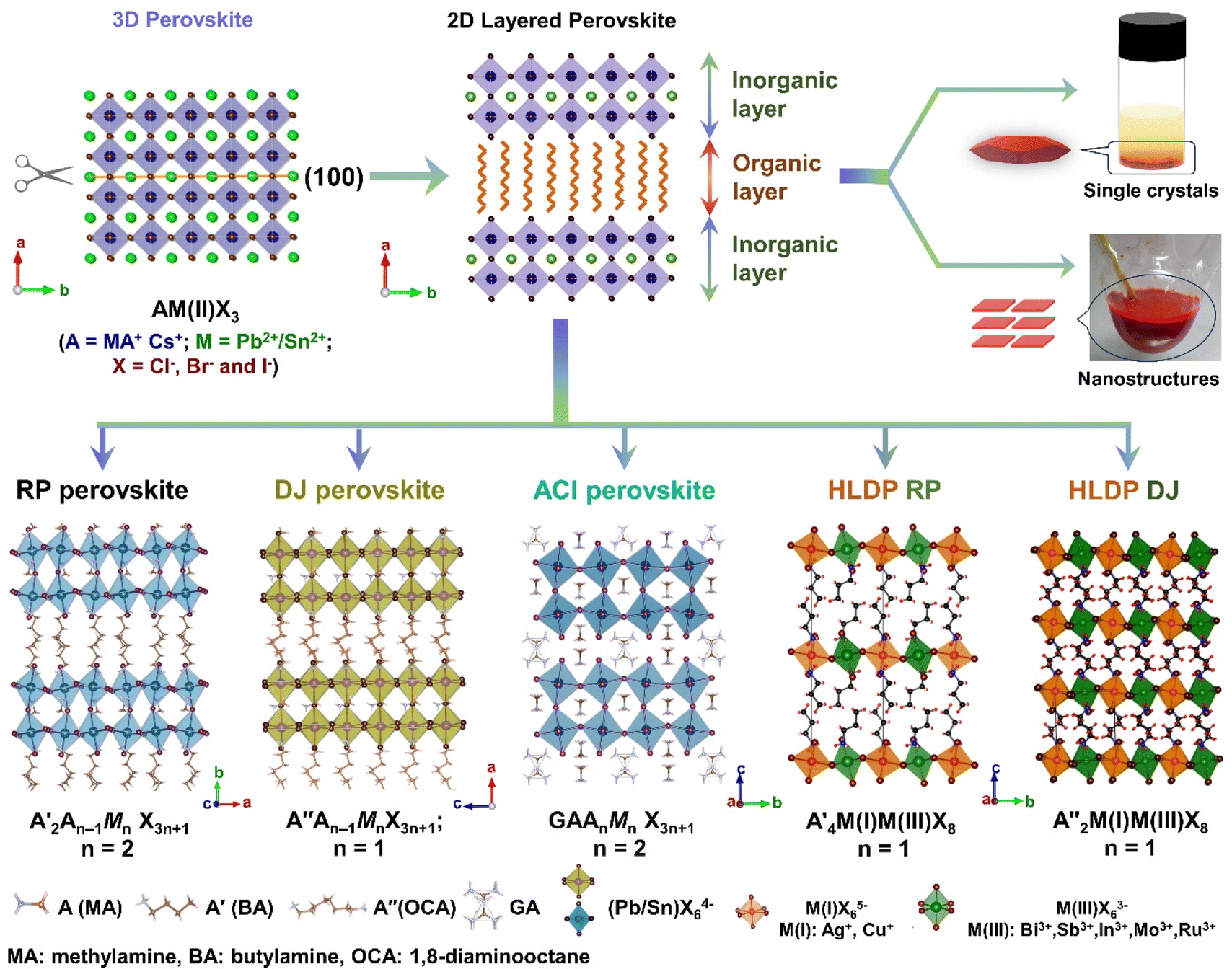 | ||
| Fig. 1 Schematic representation of the transformation from the 3D to 2D layered halide perovskites along (100), and their existence as single crystals, and NPLs (top panel). Basic structural classification of the layered halide perovskite into major categories: RP, DJ, ACI, HLDP RP, and HLDP DJ (bottom panel). | ||
In the RP phase, two parallel inorganic layers are staggered by half a unit cell (1/2, 1/2 displacement in the in-plane direction) because two successive inorganic slabs are connected by two monoammonium cations, creating a van der Waals gap between them (Fig. 1).10 In the DJ phases, the inorganic layers are joined by a single diammonium cation, resulting in an eclipsed stacking configuration where the inorganic layers are directly on top of each other (0, 0 displacement). For the ACI phase with a displacement of (0, 1/2), the inorganic layers appear eclipsed from a direction but staggered from the b direction. The A-site cation occupies the interior of the cuboctahedral cage, alternating with another cation within the lattice. Experimental observations indicate that the connectivity modes of the octahedral layers in such structures are predominantly through corner, edge, or face sharing. All of these connectivity modes are primarily governed by factors such as the nature of hydrogen bonding, the space-filling ability within the lattice, the rigidity of the spacer cations, the size of the spacer cations, and the nature of halide ions. All of these factors collectively determine the crystal structure of the 2D phase and its corresponding space groups.10 In  An−1MnX3n+1, and A′′An−1MnX3n+1, when M consists of a combination of monovalent and trivalent cations, it results in the formation of hybrid layered double perovskites (HLDP).11 The crystallization behaviour of HLDPs is contingent on the specific type of organic cation employed, resulting in the potential to exhibit either the RP or DJ phase (Fig. 1).
The incorporation of organic layers in layered halide perovskites acts as a barrier, preventing the penetration of water molecules into the crystal structures, and inhibiting halide ion migration.12,13 In conventional 3D perovskite halides (ABX3), ion migration is more pronounced due to the lower activation energy (Ea) for A+ cation, and the halide (X−).14 Conversely, the B2+ cations (either Pb2+ or Sn2+) exhibit higher Ea, and thus do not participate significantly in ion migration. The layered halide perovskites exhibit lower ion migration compared to their 3D counterparts, due to the presence of bulky organic spacers between the inorganic layers. These spacers discourage the migration of A+ cations, and hinder halide migration through the formation of strong hydrogen bonds.13 Since, the ion migration is independent of the B-site cations, both the lead and non-lead layered halide perovskites exhibit decreased ion migration.
The optoelectronic properties of the layered halide perovskites are intriguing due to their structural flexibility, which facilitates quantum confinement, dielectric confinement, exciton binding energy, carrier dynamics, tuneable band gap, and the desired band alignment.15 These systems create multiple quantum well (QW) structures characterized by varying degrees of quantum confinement, with the inorganic and organic layers acting as the well and barrier, respectively. With increasing layer numbers (n) in the inorganic slabs, the QW width is widened, which consequently decreases the band gap. This trend is advantageous for achieving longer diffusion lengths, and high carrier mobility in the photovoltaic devices. The intrinsic optoelectronic characteristics and structural orientations, and distortions can be modified by simply changing the spacer cations. This versatility paves the way for a wide range of applications, including quantum computation, LED, FET, X-ray detection and scintillation, solar cell, and photodetector.
The above dimension reduction involves a structural reorientation of the unit cell, without any analogy to the morphological reduction in nanostructures. Apart from the single crystals, the layered halide perovskites can be synthesized in the form of nanostructures, with the specific outcome depending on the chosen synthetic procedure. In general, the synthesis of single crystals involves slow cooling or slow evaporation methods,9,16 while the incorporation of surfactants in the reaction medium tends to form the nanocrystals (NCs) or nanoplatelets (NPLs).17 The dominion of a nanostructure is governed by size-dependent properties arising from the variations in crystallite size, while maintaining the same fundamental structural framework across all entities within the structure. Examples like CsPbBr3, MAPbBr3 and FAPbI3 demonstrate 3D perovskite structures, but each exhibiting distinct morphological counterparts such as NCs, nanosheets (NSs), nanorods, etc.18 For the layered halide perovskites, the thin NS/NPLs consist of inorganic blocks interconnected by organic amine spacer cations, resulting in a distinct multilayer diffraction pattern corresponding to a superlattice or superstructure. The reported 2D nanostructures are predominantly oriented along 〈00l〉, in contrast to the 2D bulk single crystals. The exploration of such perovskite superlattices is still in its early stages and has a long way to progress.
After delineating the distinctive characteristics of lead-free 2D halide perovskites in this section, our discussion in the subsequent sections commences with an exploration of the descriptors influencing the optoelectronic properties of hybrid perovskites. Following this, we delve into the structural and optical properties of low-dimensional hybrid halides. We extensively discuss the optical properties of Sn-based layered halide perovskites. Subsequently, we examine the layered halide perovskites with multiple metal centers, namely HLDP, and vacancy ordered layered double perovskites. The structural evolution of 2D superlattices is then presented. We elaborate on the optoelectronic properties, especially focusing on Sn-based layered halide perovskites, with distinct attention given to potential-biased and self-powered photodetectors. Finally, we offer our perspective on the overarching theme, highlighting the challenges in this field.
Descriptors guiding the optoelectronic properties
Band gap
The energy gap between the conduction band minima (CBM) and valence band maxima (VBM) stands out as a fundamental parameter steering the performance of any semiconductor. In layered halide perovskites, the band gap is regulated by the electronic contributions from both the inorganic block, and the organic spacer layer. Four distinct types of band alignment—type Ia, Ib, IIa, and IIb contribute to the nuanced understanding of their optoelectronic properties. In type Ia, only the inorganic slab contributes to the VBM and CBM edges, while in type Ib, the organic spacer contributes. This configuration proves advantageous for LEDs, and lasers for maintaining an optimal PLQY. Conversely, in type IIa, the CB and VB edges have contributions from the organic and inorganic layers, respectively, and vice versa for type IIb. As a result, the carriers are spatially separated into distinct layers, making this arrangement favourable for photodetectors and solar cells.19–21 A lower band gap enhances the light-harvesting capabilities, proving advantageous for photodetectors, and solar cells.The band gap of 3D perovskites can be altered by cation substitution leading to structural distortion. The band gap is expanded by introducing PbI64− octahedral tilting when a smaller cation such as Cs+ partially replaces FA+ in FAPbI3.22 Conversely, the band gap can be reduced by lattice contraction without octahedral tilting, when Cs+ partially replaces FA+ in FASnI3, whereby the absorption is extended up to the NIR region (1040 nm). As the number of inorganic octahedral layer (n) increases, the QW barrier is reduced, leading to a contraction of the band gap, regardless of whether the perovskite is in a single crystal or NC/NPL form (Fig. 2a). In the layered halide perovskites such as (HA)2(A)Pb2I7 (HA: n-hexylammonium cation), the band edge and band gap can be tuned by varying the A-site cation with Cs+, MA+, FA+, EA+, GA+, or AA+ (EA: ethyl ammonium, GA: guanidinium, AA: acetamidinium).21 In addition, a variation in the halide ion, B-site cation, and nature of the spacer molecule helps in altering the band gap.11,23,24
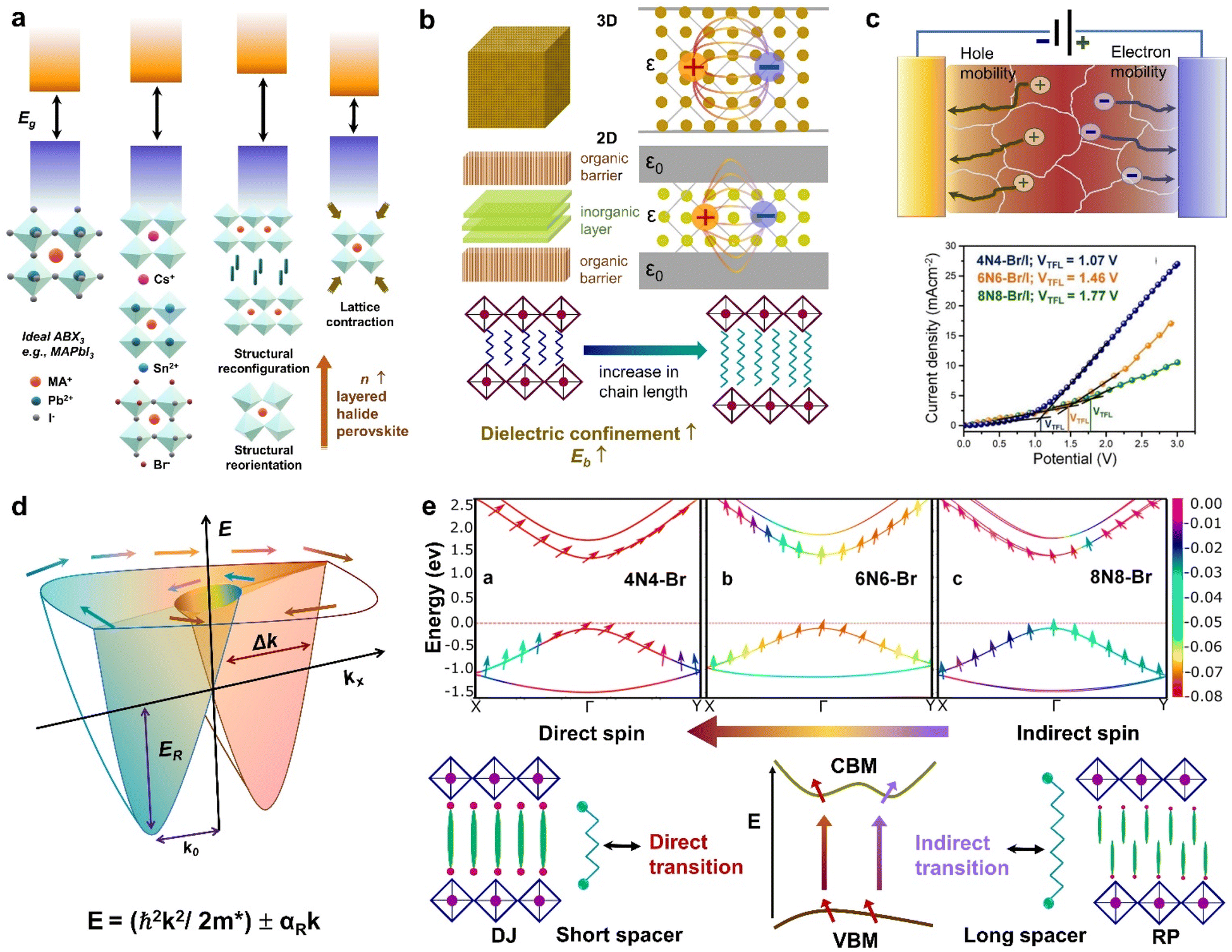 | ||
| Fig. 2 Schematic representations of the optoelectronic descriptors of 2D halide perovskites. (a) Variation of band gap with change in A, B, X sites; structural rearrangement via ligand or metal engineering; octahedral tilting; lattice contraction and variation of n value. (b) Variation of dielectric constant from 3D to 2D layered structure, and changes in spacer layer thickness. (c) Carrier mobility through a polycrystalline film in the photodetector device (top), and dark current–voltage curve by SCLC measurement, where the calculated trap-state voltage (VTFL) is directly related to the hole mobility (μ).23 (d) Rashba splitting, dictated by the strength of the Rashba SOC (RSOC) in the system: αR, and the energy splitting of the sub-bands: ΔkR = 2αRm*/ℏ2. (e) Variation of spin texture with the spacer layer thickness in DJ (xNx)SnBr4 (x = 8N8, 6N6, 4N4). The z-component of the spin (colour bar on the right) is associated with the highest occupied band, and the lowest unoccupied band along the X–Γ–Y symmetry direction (top).23 Dependence of the direct or indirect transition probability on the spin texture including the spacer layer thickness and nature of ammonium cation (RP vs. DJ) (bottom). Reproduced with permission from ref. 23, copyright (2023) American Chemical Society of Chemistry. | ||
Dielectric constant
When a material is exposed to a static electric field, its long-range charge distribution is significantly influenced by both the coulombic attraction between opposite charge centers, and the electric polarization field (P) within the material, where P = χeε0E0 (ε0: vacuum dielectric constant, χe: electric susceptibility, E0: vacuum electric field).25 The relative permittivity, or relative dielectric constant (εr) is a measure of the degree of polarization in bulk dielectrics, and is expressed as εr = 1 + χe. In halide perovskites, the excitons are bound by coulombic force, F = −e2/4πε0εrr2 where, e: electronic charge, and r: distance between electrons and holes. The dielectric confinement is strongly connected to the band gap, Eb, and the carrier mobility. In 3D perovskites with a high dielectric constant, the efficient screening of coulombic attraction between excitonic pairs leads to electrons and holes being loosely coupled in all dimensions, resulting in a reduction of Eb. In contrast to 3D systems, the layered halide perovskites display a periodic gradience in ε, alternating between the organic and inorganic layers, where εinorganic > εorganic. In layered halide perovskites, the coulombic attraction of confined excitons within the reduced inorganic well is intensified. This effect is further influenced by the screening effect of the organic barrier, which also increases the Eb.In RP (I-C6H12NH3)2PbI4, Eb was actually reduced when the ε value of the spacer molecule was increased from 3.7 to 11.1.26 This increase was achieved by the molecular intercalation of I2, which forms stable I2⋯I− interactions, and leads to the formation of (I-C6)2[PbI4]·2I2 structures within the organic layers. An elevated gradience in the ε values between the well and barrier, along with an extension in the chain length of the organic spacer cation, serves to augment the dielectric confinement (Fig. 2b).25,27 Consequently, these factors exert influence over the Eb values. The lower dimensional perovskites/hybrid halides (0D, 1D) typically display higher Eb, which is advantageous for PL properties but unfavourable for optoelectronic devices. Additionally, the enhancement of exciton dissociation and charge transport is facilitated by a higher ε, which is achieved by factors such as a greater conjugation in the organic spacer cations, extensive π–π stacking, the presence of donor–acceptor type organic spacers, and the involvement of charge transfer complexes.28
Effective mass
In a crystal, an electron or exciton interacts with the lattice potential, resulting in a response to external forces distinct from that of a free electron in free space. The effective mass thus characterizes the physical weight of a quantum particle, and its velocity under a given potential. Notably, the effective mass of an exciton is closely tied to the carrier mobility (μ) within the lattice, as expressed by μ = eτ/m* where τ represents the charge carrier scattering time, and m* denotes the effective mass of electrons or holes. The optoelectronic performance of any photoactive material is dictated by a high charge carrier mobility, a characteristic facilitated by a small m* (e, h). In addition to the optical absorption, the nature of the VB and CB, govern the effective mass, where a greater band curvature in the vicinity of the Fermi energy results in a smaller m*.29In hybrid perovskites, the moderate band gap with significant optical absorption, and the smaller m* (e, h) are dictated by the B–X bond. The B–X bond consists of the p-electron shared between the atoms giving rise to a partially filled σ bond and an enhanced optical absorption. The relative electron transfer from the B to X atoms is influenced by the overlap of the adjacent atomic orbitals, and octahedral distortions. A decreasing trend of  is observed with a decreasing band gap, and this trend is further influenced by the replacement of halides following the order I < Br < Cl < F. The m* (e, h) is expected to be higher for the layered halide perovskites, than their 3D counterparts. However, Landau level spectroscopy has revealed that the reduced effective mass (μ) of the layered halide perovskites to be smaller than that of the 3D systems.30 For instance, while the reduced mass values of FASnI3 and FAPbI3 are 0.102, and 0.09, those of (PEA)2SnI4, and (PEA)2PbI4 are found to be 0.055, and 0.091, respectively. This reduction in effective mass for Sn-based 2D hybrid halides is attributed to a favourable alignment of I p-orbitals with the 5s2 lone pair of Sn, strengthening hybridization at the VB edge.30
Carrier mobility
Carrier mobility determines the speed at which electrons or holes can move through a crystal lattice when subjected to an electric field. The ability of charge carriers to move in response to an applied electric field is crucial in various fields, particularly in photovoltaics and optoelectronics (Fig. 2c). Carrier mobility is investigated either through a combination of electrical probes, such as space charge limited current (SCLC), time of flight, Hall measurement, or by an optical probe such as transient absorption spectroscopy, time-resolved microwave conductivity, etc. Essentially, longer spacer chains may hinder the efficient movement of charge carriers within the perovskite structure, leading to reduced mobility. We have observed that the mobility in DJ Sn(II) hybrid halide perovskites decreases as the unconjugated spacer chain length increases from 4 to 8 carbons.23 In layered halide perovskites, the movement and dynamics of charge carriers are governed by ε, and the insulating barrier created by the organic spacer cations. Reducing the spacer layer thickness typically leads to enhanced carrier mobility, and a decrease in trap state density (Fig. 2c). In SCLC measurements, the carrier mobility is influenced by factors such as the thickness and crystallinity of the polycrystalline film, as well as the quality of the single crystals. The evaluation of these parameters involves the fabrication of the electron-only, or hole-only devices. The Mott-Gurney's equation is then applied, and carrier mobility is calculated from the slope of the current density vs. square of the voltage curve.23Rashba splitting
The Rashba effect, also known as the Bychkov–Rashba effect, refers to a spin–orbit phenomena, leading to a splitting of the spin-degenerate energy bands in low-dimensional materials and semiconductors with asymmetric potentials or surfaces. In the absence of the Rashba effect, electrons exhibit the same spin and momentum, but in its presence, an asymmetry in the electronic environment causes the electrons with different momenta to experience slightly different energies. The difference in energy is accompanied by spin polarization, which induces a helical spin texture of the dispersed energy, E(k), according to eqn (1):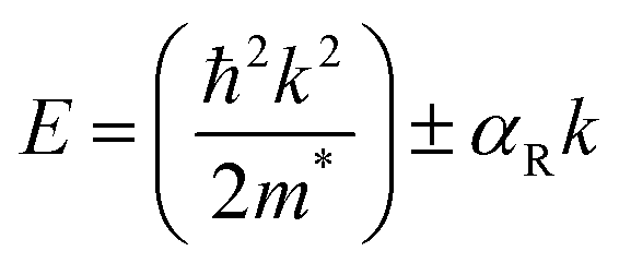 | (1) |
In halide perovskites, the local electric fields induced by the ionic defects, give rise to the inversion symmetry breaking, and Rashba-splitting. The phase transitions, and motional freedom of A-site cations can result in a local breakdown of the inversion symmetry which in turn alters the local electric field, escalating the band splitting. While Rashba splitting has minimal effect on the carrier recombination of 3D perovskites, the reduced dimension of the layered halide perovskites has a strong impact on the SOC, making Rashba effect more prominent.35 When the organic spacer cations are randomly oriented, the layered halide perovskites display a lower symmetry caused by the BX6 octahedral tilting, which triggers the band splitting in the CB and VB extrema.36 In some cases, the Rashba effect depends on the number of octahedral layers (n) in the inorganic block. A particular n value can either maintain the centrosymmetric crystal structure, showing an absence of Rashba effect, or it can lead to a broken symmetry leading to band splitting.37 The correlation between symmetry breaking, and the Rashba effect is commonly understood from techniques such as two-photon absorption spectroscopy, and angle-resolved photoelectron spectroscopy,38 beside other transient and steady-state measurements.39–41
Transition probability and spin texture
In semiconductors with a direct band gap, the optical transitions are governed by the direct transitions in k-space from the Γ-point of the Brillouin zone. Hence, the optoelectronic performance is guided by the band gap, the effective mass, or the band dispersion. Apart from the common descriptors, the spin–orbit interactions can alter the orientation of the electron spins at the states associated with the CBM, and VBM.23 Even if the spins remain direct in momentum space, the change in electron spin orientation can result in a mixture of direct and indirect optical transitions (Fig. 2e). In the context of optical transitions between the VBM and CBM, the transition probability can be determined by examining the spatial part of the wave function. The square of the expectation value of the dipole operator, when flanked between the wave functions corresponding to the VBM and CBM, provides information about the likelihood or probability of an electron making a direct or indirect transition from the VBM to CBM. In layered halide perovskites, the organic spacer molecule can regulate the admixture of the p-orbitals in the B-site cation of the inorganic block, which can lead to different spin textures at the VBM and CBM (Fig. 2e).23 Treating the electron spin classically as a vector quantity, the direct and indirect components are calculated by considering the “parallel” and “perpendicular” spins, respectively. In the absence of Rashba splitting, the spin texture argument is particularly useful in dictating the trends of optoelectronic performance of the layered halide perovskites with a library of organic spacer molecules. The manipulation of spin texture in materials, particularly in the absence of a magnetic field or ferromagnetic components, is crucial for various spin-dependent phenomena and applications in the field of spintronics.Low-dimensional hybrid halides/perovskites
Before delving into the discussion on lead-free layered halide perovskites, it is worth exploring low-dimensional hybrid halides, which encompass structures ranging from 0D to 2D. These hybrid halides are distinct from 2D layered halide perovskite structures. The class of hybrid halides captivates the scientists for their potential to exhibit unique optical, and optoelectronic properties, and therefore find broad applications across various fields such as sensing, LED, laser, X-ray detection, ferromagnetism, and ferroelectricity, etc. Lead-free metal centers with charges of +1 or +3, as well as the transition metals, often exhibit such structures. For further discussion, we have selected three distinct metal centers, Bi(III), Cu(I), and Mn(II), due to their unique and diverse optoelectronic properties, offering insight into this evolving area. These p and d-block elements often exhibit both contrasting and parallel phenomena in their optoelectronic properties. For p-block elements such as, Bi3+, Sb3+ the inorganic slabs typically exist in an isolated and confined state, separated by organic spacer cations. This arrangement enhances the electron–phonon coupling, leading to a phenomenon known as self-trapped excitonic (STE) emission. The photoluminescence (PL) band originating from the transition metal centers is influenced by multiple electronic states, Jahn–Teller (J–T) distortion, and STE emission, contributing to the complex spectral characteristics observed in these materials. Moreover, these environmentally benign, earth-abundant metal hybrid halides/perovskites demonstrate high structural stability in the ambient atmospheric conditions. Therefore, recognizing its significance, we have presented a concise overview of the structural and optoelectronic properties of low-dimensional hybrid perovskites/halides to facilitate a comparative analysis with the layered halide perovskites.Endowed with unique structural chemistry along with the optical and electronic features, the low-dimensional perovskites having a lead-free B-site metal center (e.g., Sn, Bi, Sb, In, Cu, Mn, etc.) are rapidly evolving.9,42–44 Although, Bi3+ is isoelectronic to Pb2+, its iodide version often renders the formation of vacancy-ordered perovskites because of the lack of extended connectivity between the Bi-I units. The organic cation-induced quantum barrier results in a wider optical band gap for Bi-containing perovskites, compared to their Pb-counterparts. The varying Bi-I connections, e.g., Bi2I93− (face sharing), BiI4− (edge sharing) and BiI52−(corner-sharing) also result in the isolated 0D, or quasi-2D structures.45 The introduction of conjugated spacer cations can trigger the organic–inorganic coupling, which can augment the charge transfer and photoconductivity, in the systems such as, (naphthalene diimide bis(ethylammonium))2BiI7, and (naphthalimide ethylammonium)2BiI5.46–51 Other p-block elements, such as Sb, and In, are also known to form low-dimensional hybrid halides.43,44
Apart from the p-block elements, the hybrid transition metal-halides are recognised due to their outstanding emission properties, along with their magnetic, ferroelectric, thermochromic, photochromic, X-ray detection, anti-counterfeiting, X-ray scintillation, and spintronic functionalities.42 One of the widely investigated potential candidates is the class of Cu based hybrid halide. Cu is known to exist in tetrahedral, octahedral, trigonal planar, and linear coordination environments. Although the Cu(I) systems prefer tetrahedral coordination, they can show isolated linear connectivity, e.g. (PH4P)+CuX2 (X = Cl, Br), and exist as either 0D or 1D structures. Cu(I) can also form a layered structure, such as (tBA)3Cu6I9 (tBA = tert-butyl ammonium ion), where corner-shared [Cu6I9]3− structural units are formed by common edge-sharing of six CuI4 tetrahedral units. Overall, Cu(I) halides feature linear [CuX2], tetrahedral [CuX4], trigonal planar [CuX3] building blocks and a series of polyanionic clusters of cuprous systems such as RCuX2, or R2Cu4X6 (R = organic cations).52 Besides the excellent Cu-based hybrid halide emitters, there are a few non-luminescent Cu-based hybrid halides, namely, PyCs3Cu2Br6, and (PH4P)+CuX2, where the organic cations have a detrimental impact on the PL quantum yield (PLQY). On the other hand, the layered C6H10N2[CuCl4] has been proven to be a promising photoabsorber.
In the Mn(II) halide category, Mn2+ displays red and green emission depending on the strong-field octahedral, and weak-field tetrahedral coordination environments, respectively. In the hexacoordinated systems, one Mn2+ and six X− ions combine to form the point, edge or face sharing [MnX6]4− octahedra which are classified into 0D, 1D, and 2D hybrid halides.53 The [MnX4]2− tetrahedra, initially exhibiting green emission, can undergo changes in its chemical environment through tetrahedral tilting, or by an external stimulus such as pressure, resulting in a shift from green to yellow, orange, and red emission. Mn(II) hybrid halides have high PLQY which is beneficial for commercial LEDs and WLED chips. The octahedrally coordinated red emitting (C4H12N)MnCl3, (CH6N3)2MnBr4 and tetrahedrally coordinated ((C8H20N)2MnBr4), (C8H34P2)MnBr4 achieve 91.8%, 61.9% and 81.5%, 95% PLQY, respectively. The absorbance or PL excitation (PLE) spectra are mainly attributed to the multiple electronic transitions, from the 6A1(S) ground state to the 4A2(F), 4T1(F), 4T1(P), 4E(D), 4A1, 4E(G), 4T2(G), and 4T1(G) excited states.53 The 4T1 → 6A1 transition is responsible for the bright emission of these systems. When the Mn2+- halide polyhedral units are surrounded by non-conjugated or less conjugated organic cations, it results in a type-I band alignment. In case of the conjugated systems, the lowest unoccupied molecular orbital (LUMO) is too low for a type-I alignment, which in turn results in PL quenching.
When water molecules are present in the lattice of the lead-free hybrid structures e.g., (propanediammonium)2Bi2I10·2H2O, and (t-BA)2Cu2I4·H2O, the interaction between the inorganic block, and spacer cation is weakened by the hydrogen bonding with the organic cation.54 This in turn alters the chemical environment which affects the optoelectronic properties. Recently, macromolecules, or crown ether caged metal polyhedral halides have become a potential alternative of traditional hybrid perovskites because of their high PLQY, and ambient stability.
Sn-based layered halide perovskites
Sn-based 2D hybrid perovskites frequently exhibit a 〈100〉 orientation, and are considered among the most promising lead-free alternatives in the p-block. In the presence of GA+ with MA+ or Cs+ cations, the Pb-based hybrid halide adapts the ACI phase having 〈110〉 orientation.15 The 〈110〉 oriented structure was obtained for [NH2C(I)![[double bond, length as m-dash]](https://www.rsc.org/images/entities/char_e001.gif) NH2]2(CH3NH3)mSnml3m+2 (m = 2–4), (C(NH2)3)2SnI4, α-(NH3C5H10NH3)SnI4α-(HA)SnI4 (HA = histammonium), and with 1,3 propane diammonium cation having the bromide counterpart.55 Sn-halide perovskite single crystals are conventionally synthesized by the acid precipitation method at a slightly elevated temperature, where the precursors (metal salts, and amines, or pre-prepared amine-salts) are taken in a specific molar ratio, dissolved in an adequate amount of acid (HI, HBr, HCl), commensurate with the halide composition. The single crystals are obtained by slow cooling of the solution. The single crystals can also be generated by the antisolvent method, or slow evaporation over extended periods.
NH2]2(CH3NH3)mSnml3m+2 (m = 2–4), (C(NH2)3)2SnI4, α-(NH3C5H10NH3)SnI4α-(HA)SnI4 (HA = histammonium), and with 1,3 propane diammonium cation having the bromide counterpart.55 Sn-halide perovskite single crystals are conventionally synthesized by the acid precipitation method at a slightly elevated temperature, where the precursors (metal salts, and amines, or pre-prepared amine-salts) are taken in a specific molar ratio, dissolved in an adequate amount of acid (HI, HBr, HCl), commensurate with the halide composition. The single crystals are obtained by slow cooling of the solution. The single crystals can also be generated by the antisolvent method, or slow evaporation over extended periods.
Given that the standard reduction potential for the Sn4+/Sn2+ couple is only +0.15 V, Sn2+ tends to be oxidized to Sn4+ under standard conditions. To restrict the oxidation of Sn2+ to Sn4+ state, excess H3PO2, and SnF2 (as an additive) are employed in the acid precipitation method. Notably, for the Sn-based 2D halide perovskites, discussed in this perspective, the presence of Sn(IV) is negligible compared to Sn(II). The quantification of Sn(IV) was achieved by analysing the area under X-ray Photoelectron Spectroscopy (XPS) plots. Specifically, in Sn-containing layered halide perovskites with mixed halide compositions (such as 8N8-Br/I, 6N6-Br/I, and 4N4-Br/I), Sn(IV) is absent in the XPS plots of Sn 3d level. However, in pure iodide samples (e.g., 8N8-I), a small proportion of Sn(IV) was detected, with a calculated fraction of Sn(IV) as 0.03. Furthermore, the superlattice nanostructures also did not exhibit the Sn(IV) state in XPS analyses.
Optical properties
The optical properties of Sn-based layered halide perovskites are governed by the halide composition, the type of organic spacer cation, spacer layer thickness, molecular intercalation, and the electron–phonon coupling that leads to the formation of STE states. The RP or DJ Sn-based bromide systems usually show the optical absorption below 450 nm, and a broad intense emission with large stokes shift at room temperature.9 The DJ perovskite with the 1,8-diammonium octane (8N8) spacer, experiences a blue shift of the absorption onset with a reduced optical density as the band gap is enhanced from the iodide to the mixed halide, and the bromide counterparts (Fig. 3a).23 The PL emission band is also blue shifted from iodide to bromide (Fig. 3b). The emission band positions are independent of the excitation wavelength (λex), although the PL intensity is enhanced at lower λex. The DJ perovskites has an inherent structural stability in having the hydrogen bonding in between the divalent spacer molecule, and the SnX6 octahedra. On the contrary, the RP counterpart consists of an insulating gap between the protonated n-octylammonium (8N) spacer cation held together by van der Waals interaction, which in turn deteriorates their optoelectronic performance. Both DJ (8N8)SnBr4 (8N8-Br), and RP (8N)2SnBr4 (8N-Br) have appreciable PLQY of 99.7 ± 0.3%, and 91.7 ± 0.6%, respectively. While the 8N8-DJ retains the PLQY even after one month storage under ambient conditions, the PLQY of 8n8-RP continuously drops with time (Fig. 3c and d). The stronger H-bonding interactions and absence of van der Waals gap offer greater stability for the DJ perovskites compared to the RP counterpart.56 Reducing the spacer layer thickness through the use of 1,6-diammonium hexane (6N6) and 1,4-diammonium butane (4N4) spacers maintains a comparable absorption onset, indicating a proximity in their band gaps. However, noteworthy alterations are observed in the optical density, as illustrated in Fig. 3e, accompanied by changes in the emission profile. 4N4-DJ shows a narrow band edge (BE) emission with low Stokes shift, whereas for 6N6-DJ and 8N8-DJ, the emission band is broadened due to the STE emission (Fig. 3f).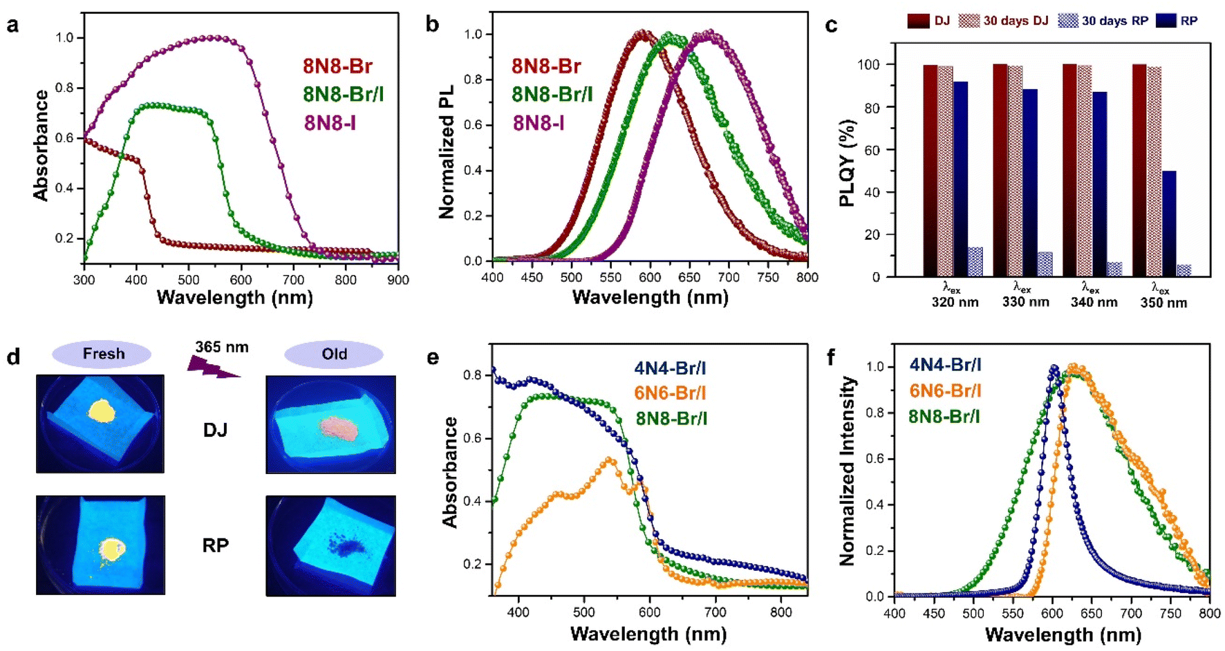 | ||
| Fig. 3 (a) UV-vis absorption, and (b) PL spectra of (8N8)SnX4 (X = Br− and/or I).23 (c) Bar plots showing the ambient-stability of PLQY between the fresh and 30 days stored DJ (8N8)SnBr4 and RP (8N)2SnBr4 samples under relative humidity of 55% and 25 °C, at different λex.9 (d) Digital images of the corresponding DJ (8N8)SnBr4 and RP (8N)2SnBr4 crystals showing better ambient stability of the DJ perovskite.9 (e) UV-vis absorption and (f) PL spectra at λex = 360 nm for xNx-Br/I (x = 8N8, 6N6, 4N4) Sn-mixed halide DJ perovskites.23 Reproduced with permission from ref. 9 and 23, copyright (2022 & 2023) American Chemical Society of Chemistry. | ||
The structural conformation and optical properties of the Sn(II) layered iodide perovskites can also be tuned by the reversible molecular intercalation–deintercalation with the spacer cations.57,58 The intercalation of benzene (C6H6) is possible in 2,3,4,5,6- pentafluorophenethylammonium bilayers to form the (C6F5C2H4-NH3)2SnI4·(C6H6) crystal.57 Conversely, fluorinated benzene (C6F6) can be inserted in between the phenethylammonium bilayers forming (C6H5C2H4NH3)2SnI4·(C6F6). Also, the intercalation and deintercalation of molecular I2 in (A)2PbI4 is reduced with increasing spacer chain length of the A+ cation.58 Here, the I2 intercalated crystal shows two absorbance and emission peaks whereas, the pristine crystals display only one peak in the absorbance and emission profiles. Such a phenomenon has significant impact on the photochromism, sensing, and conductivity of the devices.
STE emission
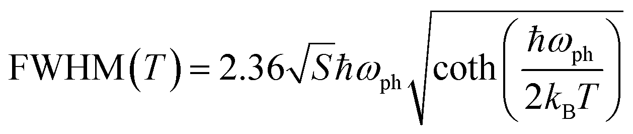
At a specific excitation power, a stable equilibrium in the population density of bound, free, and trapped excitons is established prior to their radiative relaxation. The density of these charge carriers is contingent upon factors such as the rate of photocarrier generation, the lifetimes within their respective states, and the intensity of excitation.59 STE emission involves the transfer of charge carriers from the CBM to these overlapped states, and subsequent emission to the 1S0 ground state. The luminescence of layered halide perovskites mostly originates from the defect scattering, and optical phonon scattering, except for the BE emission. The scattering processes involving the electrons, optical and acoustic phonons contribute to the attainment of thermal equilibrium, which in turn influences the electronic band structure, and leads to modifications in the PL spectra. These scattering processes are responsible for the thermal variation of the full-width at half-maximum (FWHM) of the PL bands.One of the conventional methods for analysing the electron–phonon coupling is to evaluate the FWHM of temperature-dependent PL spectra, according to eqn (2):9
 | (2) |
 | (3) |
The overlapped delocalised states below the CBM, and the corresponding STE emission are responsible for the higher PLQY of 8N8-Sn (RP/DJ).9 With a λex of 380 nm, the intensity of the yellow STE emission band at 580 nm increases with increasing temperature. Below 100 K, the 440 nm BE emission is observed (Fig. 4a). This BE is both spin and parity allowed, and occurs from the 1P1 excited state to 1S0 ground state which is common for the B-site cations with ns2 configuration. At temperatures below 100 K, where excited electrons possess lower thermal energy, the carrier–phonon coupling becomes less influential, leading to a reduced intensity of the STE band compared to the BE emission. As the temperature rises, the excited electrons gain thermal energy, enabling them to surpass the activation energy for transport from CBM to the STE state. The dominance of the STE band over the BE emission occurs at λex < 380 nm, while at higher λex, only the BE emission band is observed (Fig. 4b). Regardless of temperature, the STE emission is more prominent at lower λex, since the electrons can be excited to higher vibrational energy states, facilitating their transfer to the delocalized STE states, making the STE emission more favourable. The position of the BE emission peak remains temperature-independent at each λex. However, the STE emission experiences a blue shift between 5 and 75 K, followed by a red shift up to 300 K. This variation in the STE peak position is attributed to the interplay of competing effects of thermal expansion, and electron–phonon interactions. At λex of 360, 380, and 400 nm, the calculated Eb values are 34.7 ± 1.2, 35.0 ± 0.8 and 37.3 ± 1.5 meV, respectively. The fact that the Eb values are independent of λex, suggesting a favourable electronic transition from the free exciton state (FE) to the free carrier state (FC). This characteristic is crucial for a facile electron extraction process.
 | ||
| Fig. 4 (a) PL spectra of (8N8)SnBr4 in the range 5 to 150 K, at λex = 380 nm.9 Schematics of (b) the energy level diagram demonstrating the BE and STE emission,9 and (c) the exciton self-trapping in the perovskite lattice. (d) FWHM (in eV) as a function of temperature at λex of 360 and 380 nm for (8N8)SnBr4.9 (e) Schematics showing the broad emission through the sub-band gap states, which are present in a system with stereochemically active ns2 lone pairs, along with a parallel phenomenon of J–T distortion, together promoting the STE. Reproduced with permission from ref. 9, copyright (2022) American Chemical Society of Chemistry. | ||
Structural impact on STE emission
The selection of the organic spacer cation induces variations in the parameters such as Eb, dielectric constant (ε), and the electronic band structure. Transitioning from the aromatic to aliphatic monoammonium cations, and with an increase in the organic spacer layer thickness, the band gap increases.59 The aromatic ammonium cations forestall the thermal movement between the inorganic octahedral layers due to the strong CH–π stacking of the aromatic rings. Nevertheless, the presence of alkyl chains induces varying degrees of distortion in the inorganic octahedra, leading to alterations in the density of defect states. This, in turn, promotes electron–phonon coupling within the system through structural distortions, lattice vibrations, and thermal movement between the inorganic layers. The scattering effect due to the charged defect states is prominent in reducing the PLQY of (PEA)2SnI4, (BA)2SnI4, (HA)2SnI4, and (OA)2SnI4 [PEA: ph, BA: butylammonium cation, HA: hexylammonium cation, OA: octylammonium cation].59 Elliot's theory provides substantial qualitative information on the Eb, and ε values of organic cations which further shows that the εA for an aromatic spacer is smaller than the alkyl ammonium cation.59,61,62 Furthermore in layered halide perovskites, a strong coloumbic interaction between the bound excitons is responsible for the lesser value of εA (A: spacer) than εw (W: Sn-octahedra). These two factors contribute to the lower Eb observed in (PEA)2SnI4, compared to its alkyl spacer counterparts.A strong correlation exists between the structural factors, and the electron–phonon coupling (Fig. 4c). The rigidity of different structures can be distinguished by extracting the atomic displacement (Ueq) in the single crystals. The higher values of Ueq, and Γ(LO) observed in (OA)2SnI4 in comparison to (PEA)2SnI4 indicate a greater contribution of STE emission in the alkyl chain systems.59,63–66 This is attributed to the defect states, resulting in the intraband PL, and a subsequent loss of PLQY. Since STE depends on the octahedral tilting in the inorganic layer, the PL intensity also increases with higher out-of-plane octahedral tilting. Increasing the chain length of the organic spacer cations also enhances the compressive strain as well as the degree of octahedral distortion (8N8 > 6N6 > 4N4).9 The highest out-of-plane octahedral distortion increases the electron–phonon coupling. From the fitted FWHM (in eV) as a function of temperature, the numerical value of S, ℏωph are calculated (Fig. 4d).
Jahn–Teller distortion
A vast majority of the halide perovskites have a reduced crystal structure symmetry due to the lattice distortions, and the J–T distortion leading to octahedral tilting. This leads to the hettotypes, where the overall perovskite framework is preserved like the aristotype, but having a lower symmetry.67 In particular, the rock-salt-ordered double perovskite structure is stabilized by the J–T distortion, that splits the unequally occupied eg orbitals, and lowers the energy of the octahedral units.68 In contrast to the electronic transition arising from the J–T distortion in Cu(II), with d9 electronic configuration, there are two possible conditions when the J–T inactive Cu(I) can display the electronic transitions. The first is the temporary oxidation of the d10 system into d9 configuration by photoexcitation. The second criterion is the relaxation of the Laporte selection rule by mixing the d-orbitals with s- and p-orbitals in the complex hybrid structure. This J–T distortion results in antiferrodistortive arrangement in the coordination environment of the inorganic layer. When photoexcitation promotes an electron into Cu-4s orbital leaving a hole in the 3d orbital, the J–T distortion escalates the electron–phonon coupling (Fig. 4e).The 0D (Ph4P)CuX2 displays STE emission, since the charge is localized within the isolated [CuX2]− units. On the other hand, the (tBA)CuX2 (X = Cl, Br) having a similar structural configuration, displays cyan-green emission exhibiting PLQY of 92.8% for X = Cl−, and 80.5% for X = Br−, while (tBA)CuI2 is a white light-emitter with a PLQY of 54.3%.69 In the iodide system, dispersive Cu-4s states contribute strongly to the CBM, and thereby the J–T distortion creates intrinsic self-trapped states, overruling the STE emission.70 The manganese containing hybrid halides usually contain Mn2+ centers with d5 configuration, giving rise to multiple excited electronic states. The green emission originates from 4T1 → 6A1 transition, and the red emission is due to the ferromagnetic coupling between two neighbouring Mn2+ ions. When the thermal vibration of the lattice is minimized, the non-radiative trap-state induced transitions are reduced which enhances the PLQY. The PLQY can reach up to 81% for [P14]2[MnBr4] (P14: N-butyl-N-methylpyrrolidinium cation).71 However, the appreciable PLQY in various hybrid halides containing Sn, Cu, Bi, Sb, etc., is attributed primarily to the electron–phonon coupling.
The photo-oxidation-driven, or the J–T distortions generate the intrinsic STE states in transition metal-based systems, while the lattice deformations or vacancies create the extrinsic STE states in p-block systems. Besides the electron–phonon coupling, the electronic contribution of vacant (n − 1)th d- and nth s-orbitals cannot be ignored to decide the nature of emission. In the Sn2+ perovskites, a stereochemically active ns2 lone pair creates the dynamic J–T distortion. The ns2 ions are present as a parent or dopant center, whereas the excited sp state contains lower 3P state which can either undergo a dynamic J–T distortion, or a strong spin orbit coupling, splitting the sp state into the 3P0, 3P1, and 3P2 states. While 1S0 → 1P1, and 1S0 → 3P1 transitions are complete, and partially spin-allowed, respectively, 1S0 → 3P2, and 1S0 → 3P0 are the forbidden transitions. However, the dynamic J–T distortion in 3P1 state along with the off-center position in 1S0 ground state, result in a broad band 1S0 → 3P1 emission with large stoke shift (Fig. 4e).72 Since the dynamic J–T distortion also enhances the electron–phonon coupling, the origin of the transitions can be either STE, or STE-like 3Pn (n=0, 1, 2) → 1S0. The temperature-dependent dynamic charge transfer is also observed in hybrid halide perovskites, and such as charge transfer, or defect scattering is arduous to be distinguished from STE.73 Although, these phenomena are interconnected, the dominant factor governs the optical properties, depending on the perovskite lattice.
Polaronic effect
The polaron can be expressed as a quasiparticle resulting from the interaction between an electron (or hole), and the polarizing field in a crystal lattice. The self-trapping of charge carriers is possible when they experience a coulombic interaction with the relatively heavy, and slow-moving atoms. The self-trapped carrier remains bound in the potential well produced by the shift from the equilibrium position of the atoms. This displaceability of the ion is quantified by the ratio of static to high-frequency ε, which is almost ten times higher in halide perovskites as compared to other ionic, and covalent materials. These relaxed charge carriers are broadly termed as polaron, and classified according to the interaction governing the potential well depth, and size.Fröhlich-like large polaron shows a narrow peak corresponding to the free excitons (FE), whereas the Holstein-like small polarons having fundamentally different features, are attributed to the STE with high stokes shift, and substantial lattice distortion.74,75 A small polaron localised in a confined lattice site enables the interaction between the charge carrier and phonon. The halide perovskites have low frequency LO phonon mode due to the presence of heavy metal ions. The linewidth of the phonon absorption is generally broad at room temperature which is an indication of phonon overdamping. The soft lattice nature of halide perovskites creates large phonon anharmonicity which causes this overdamping.76 Any local distortions i.e. bond angle or bond length variation, inorganic framework tilting, or doping, modify the coulombic interaction forming the small polarons. The incoherent atomic motion localizes the charge carriers, and alter the parent band structure. In this context, the potential depth of the STE state from the CBM is vital to direct the optical properties of halide perovskites. When the energy of self-trapping depth (Edepth) is large, the de-trapping of carriers and back transfer from STE to CBM is an energetically unfavourable phenomenon. However, the back transfer becomes allowed, when the barrier is small. If Eb is greater than the thermal activation energy (26 meV at room temperature), BE emission dominates over the STE emission.
2D halide perovskites with multiple metal centers
Participation of two discrete metal centers in HLDPs
In HLDPs, the alternate octahedra of the inorganic layer are constituted of heavy main group trivalent metal centers such as M(III): Bi3+, Sb3+, or In3+, and the monovalent M(I) ions: Ag+ (Fig. 5a).11,77 The inorganic layers are separated by a single, or double layer of organic amines to generate the RP and DJ phases, respectively. The HLDP structure can be visualized to be derived from the double perovskites [Cs2M(I)M(III)X6] by slicing along (100) planes, to generate the 〈100〉 oriented ( /
/ )M(I)M(III)X8, where the bulky organic spacers are denoted by a monoamine (A′), or diamine (A′′).42 The DJ HLDP structures,
  AgM(III)X8 may also consist of Mo3+, Ru3+, and Fe3+, having distinct magnetic properties.78,79 The HLDPs are also stabilized by the hydrogen bonding interactions between the halide ions, and the NH3+ groups of the organic spacer. 1,4 Diamino butane (4N4) in combination with Ag(I)/Bi(III), and Ag(I)/Sb(III) pairs forms stable HLDP phases.11 Changing the 4N4 to a bulkier diammonium spacer (1,6 diamino hexane; 6N6) alters the HLDP phase into the 1D (6N6)SbBr5. The 1D structure do not contain any Ag+ center, because of its higher ionic radius of 1.15 Å, that does not allow it to be accommodated in the neighbouring octahedra along with Bi3+ (1.03 Å), or Sb3+ (0.76 Å). On transitioning from the bromide to iodide composition, the iodide phases with Ag(I)/Bi(III), and Ag(I)/Sb(III) are also devoid of Ag+, because of the reluctance of Ag+ to form AgI65− octahedra.80 There are only a very few reports where aerometric interactions between aryl amines that stabilize the iodide HLDPs to form (AE2T)2AgBiI8 {AE2T = 5,5-diylbis-(aminoethyl)-[2,2-bithiophene]), and [(R/S)-β-MPA]4AgBiI8 [(R/S)-b-MPA = (R/S)-(±)-b-methylphenylammonium].80,81
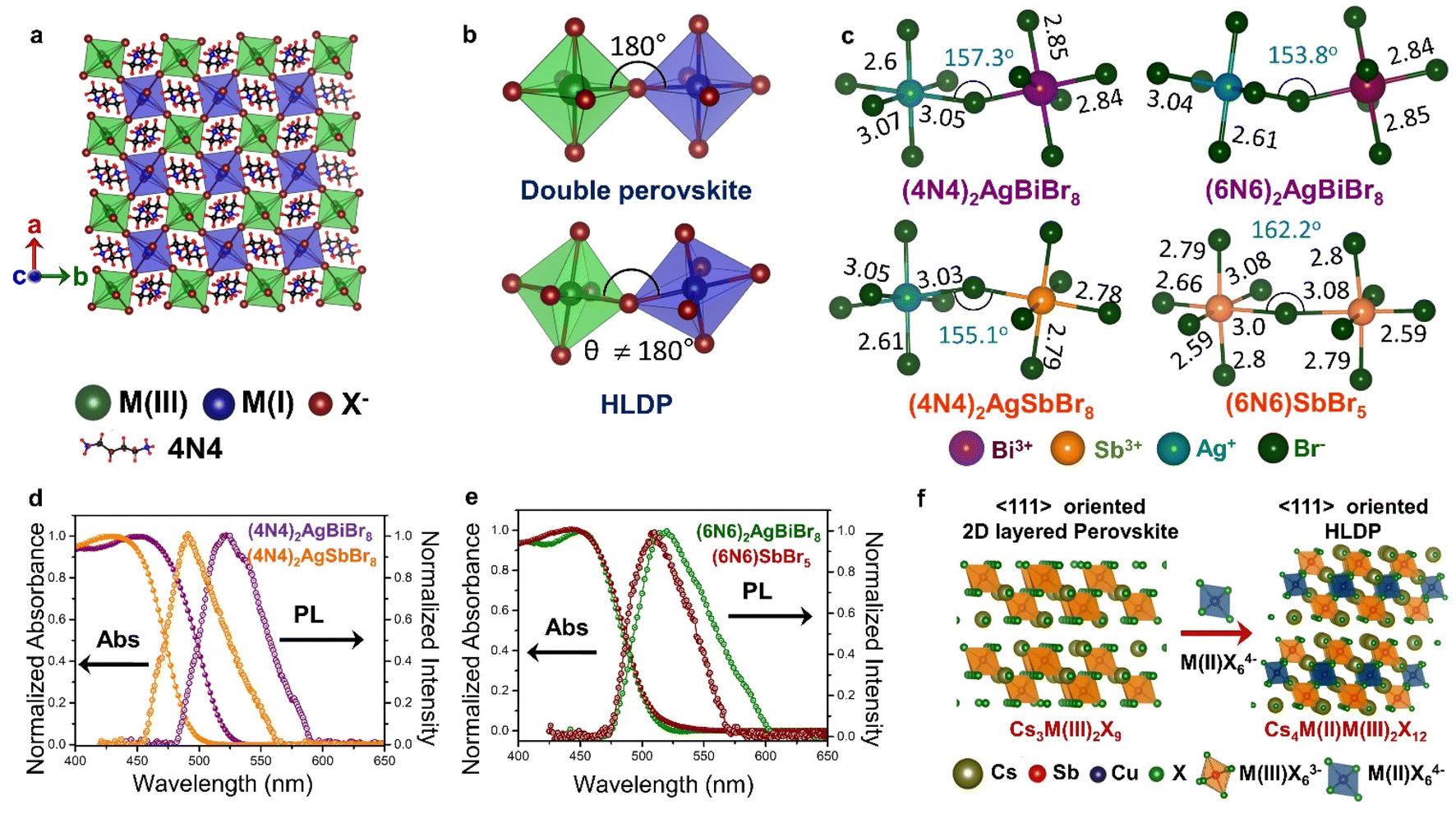 | ||
| Fig. 5 Schematic representation of (a) the octahedra with M(I) and M(III) centers in the inorganic layer of double perovskite, and HLDP, and (b) the corresponding octahedral tilting. (c) Variations of bond length (in Å) and bond angle (in degrees) in (4N4)2AgBiBr8, (4N4)2AgSbBr8, (6N6)2AgBiBr8, and (6N6)SbBr5.11 Optical absorption, and PL spectra of (d) (4N4)2AgBiBr8, and (4N4)2AgSbBr8, and (e) (6N6)2AgBiBr8, and (6N6)SbBr5.11 (f) Schematic for the formation of LDPs from single layered 〈111〉 oriented perovskites. Reproduced with permission from ref. 11, copyright (2023) Royal Society of Chemistry. | ||
Unlike the 3D double perovskites having M(III)-X-M(I) angles of 180°, the HLDPs exhibit considerable octahedral tilting (Fig. 5b), and a variation of bond lengths, especially due to extreme bond length variations in the AgX65− octahedra (Fig. 5c).78 Due to the alternately placed MBr63− and AgBr65− octahedra, a higher degree of octahedral tilting is observed for the HLDP structures as compared to the 1D (6N6)SbBr5 (Fig. 5c). The octahedral distortion also increases, when the spacer layer thickness increases from 4N4 to 6N6. As mentioned previously, the nature of the organic spacers, monoamine or diamine, as well as the spacer chain length, determine the stacking pattern of the respective octahedra. While 4N4 always forms the DJ-type HLDPs, where the inorganic layers lie on top of each other in the (0,0) pattern, the inorganic layers connected by the monoammonium cations, shift to form (1/2, 1/2) stacking in the RP analogues.42 The HLDPs having smaller diamine spacers, such as 1,3 diamino propane, exhibit the (1/2, 0) type stacking pattern.78
The optical properties of the HLDPs are primarily controlled by M(III), more than the spacer (Fig. 5d and e). The bromide HLDPs usually display absorption edges below 500 nm. The substitution of Bi3+ with Sb3+ or In3+ causes a bluer shift of the absorption edges. The absorption and PL spectra do not differ much with the spacer chain length (Fig. 5d and e), but are red shifted from bromide to iodide, since the red-coloured iodide HLDPs display absorption edges above 600 nm. In contrast, the chlorides exhibit a wide range of absorption, from UV to near IR, depending on the metal composition. The Ag(I)/In(III) HLDP chlorides with band gap above 3 eV absorb in the UV region. When In(III) is replaced by Mo(III) or Ru(III), the band gap is lowered below 2 eV. HLDPs display compelling electronic properties in terms of direct and indirect band gaps, depending on the trivalent metal center, and the amine spacers. The Ag(I)/Bi(III) HLDPs with 4N4 spacer [(4N4)2AgBiBr8] exhibit direct band gap, unlike the 3D counterpart, i.e., Cs2AgBiBr6.11 The indirect to direct band gap transition, with the lowering of dimensions, can be explained by molecular orbital theory. For example, the contribution of only Ag-s orbital at the valence band maximum (VBM), and Bi-p orbital at CB leads to direct band gaps.8 The nature of the band gap also depends on the metal center, such as Ag(I)/Sb(III) HLDPs display direct band gaps,11 whereas Ag(I)/In(III) HLDPs have indirect band gaps.77 With the increase of spacer chain length from 4N4 to 6N6, the band gap can also change from direct to indirect.
Vacancy ordered layered double perovskites
Besides the 〈100〉 oriented HLDPs, the 〈111〉 oriented layered halide perovskites are created by introducing vacancy. By substituting M(I) in Cs2M(I)M(III)X6 with M(II), and a vacancy, 〈111〉 oriented Cs4□M(II)M(III)2X12 (□ = vacancy and M(II) = bivalent metal center) can be obtained.82 The layered double perovskites (LDPs) are also known as multiple-layered 〈111〉 perovskites. The single layered 〈111〉 oriented Cs3□M(III)2X9 is converted into the LDP, by the incorporation of M(II)X64− octahedra (Fig. 5f). In Cs4CuSb2Cl12 with a band gap of ∼1 eV, Cu2+ exhibits near IR absorption,82 whereas the Cd2+ or Mn2+ centers in Cs4CdSb2Cl12 and Cs4MnSb2Cl12 increase the band gap.83,84The alloying of metal centers is another prospective method to tune the optoelectronic properties of the layered halide perovskites. The high-entropy alloying in vacancy-ordered cubic double-perovskite, Cs2MCl6 (M = Zr4+, Sn4+, Te4+, Hf4+, Re4+, Os4+, Ir4+ or Pt4+), produces multiple distinctly isolated octahedral units, giving rise to the complex vibrational and electronic structures.85 Instead, the B-site alloying is regulated by thermodynamic factors. In RP (BA)2(MA)n−1PbxSnn−xBr3n+1, and DJ (3AMPY)(MA)n−1PbxSnn−xBr3n+1 (n = 1–3), the Pb2+-rich layer is more thermodynamically favoured, whereas, when n = 1, alloying of Sn2+ becomes difficult. At higher n values, the probability of B-site alloying increases, with a simultaneous variation in the electronic and optical properties.86
2D nanostructures
In layered halide perovskites, the inorganic octahedral layers connected by the organic ammonium cations, are often assembled in a harmonic periodic array, transforming the inorganic building blocks into periodically stacked NPLs, forming a superstructure, also referred to as perovskite superlattice.17 The formation of a superlattice depends on the synthetic methods, such as template-based slow evaporation, ligand-assisted reprecipitation (LARP), standard hot injection (HI) method, etc. In the LARP method, the precursor salts and the organic acid–base pair, or the pre-synthesized single crystals are dissolved in a solvent, followed by the addition of an antisolvent (e.g., toluene, isopropanol) for the precipitation of the NPLs. While the organic amine molecule acts as the spacer cation, the acid counterpart passivates the nanostructure surface. The inclusion of two amine spacer molecules thereby changes the periodicity (Λ) of the NPL stacking.87,88 In the HI method, a low enough temperature, and the precision in selecting the ratio of organic acid and amine pair are crucial for stabilizing the superlattice.89 The intended 2D phase can also be achieved by introducing a foreign metal at the B-site (Fig. 6a). Designing the inorganic layers with the combination of two metal centers, is a bit tricky art for the NPL superlattice assembly.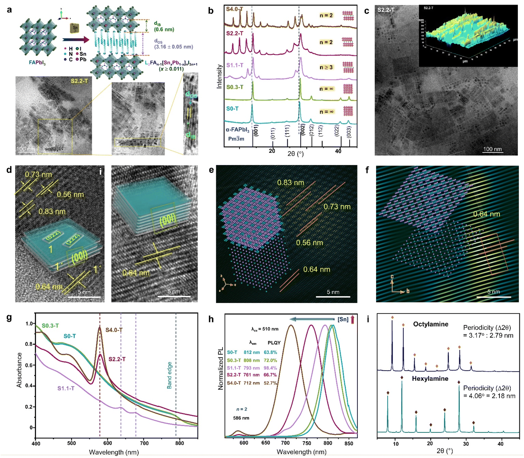 | ||
| Fig. 6 (a) Schematic showing the transformation of 3D FAPbI3 NCs to 2D RP superlattice of L2FAn−1[SnxPb1−x]nI3n+1 (x ≥ 0.011), and the TEM analysis of S2.2-T NPL superlattice. Sequentially magnified TEM images show the superlattice structure, and its correlation with Λ = dIB + dOS = 4.35 ± 0.06 nm. IB and OS represent the inorganic block with n = 2, and the organic spacer, respectively. (b) PXRD patterns with increasing Sn/Pb ratio, illustrating the gradual phase change from cubic NCs to 2D RP NPLs. (c) TEM image, and AFM image (inset) for the S2.2-T superlattice. (d) TEM images and schematics showing the NPL stacking with (i), and without (ii) edge offset. FFT mask filter analysis of the NPLs with (e) edge offset stacking, and (f) perfect stacking. The lower left insets show the model crystal lattice of a single NPL, and upper left insets demonstrate the stacking of four lattice planes. (g) Optical absorbance spectra, and (h) PL spectra (λex = 510 nm) of S0-T, S0.3-T, S1.1-T, S2.2-T and S4.0-T. (i) XRD patterns of the RP NPLs (x = 0.022, n = 2) with hexylamine and octylamine as the spacer. Reproduced with permission from ref. 89, copyright (2023) WILEY-VCH Verlag GmbH & Co. KGaA, Weinheim. | ||
One of the unique features of these 2D superlattices is the multilayer diffraction, similar to those of the NCs, packed with a periodic layout.17 Here the split is mostly observed at the first Bragg peak, but not for the second. The X-ray scattering from a periodic packing of the NPLs results in interference fringes due to the constructive interference between the scattered X-rays from neighbouring NPLs. The degree of stacking in such an ordered structure influences the multilayer diffraction. The NPLs made by the inorganic octahedra constitute the most electron-dense part, resulting in stronger diffraction intensity, and higher scattering factor compared to the organic spacer. The superlattice periodicity (Λ) can be extracted directly from Bragg's diffraction. The scattering (momentum) vector q (nm−1), and the order of the superlattice reflection (n) are related to the Bragg angle (θ), and X-ray wavelength (λ), according to the following equations:
 | (4) |
2![[thin space (1/6-em)]](https://www.rsc.org/images/entities/char_2009.gif) sinθn = nλ/Λ sinθn = nλ/Λ | (5) |
| qn = 2πn/Λ | (6) |
Since the peaks are periodic, Λ is related to Δq, according to eqn (7):
| Δq = qn+1 − qn = 2π/Λ | (7) |
From the Gaussian fit profile of the multilayer diffraction and corresponding q vs. n plot, Λ, and the organic layer thickness can be evaluated. Λ measures the extent of disorder with two major contributing parameters, σL (inhomogeneity of the organic layer), and σN (NC/NPL stacking fault). An ordered face-to-face arrangement of the NPLs decreases the σL (∼0.5), compared to the NCs. The multilayer diffraction of assembled NCs or NPLs becomes evident from small angle X-ray scattering, and grazing incidence wide angle X-ray scattering.90 However, the NPLs are not adequately described by a unit cell or structure factor because of their crystal truncation, and different surface terminations.
The introduction of Sn2+ in the virgin structure of FAPbI3 results in the transformation of FASnxPb1−xI3 (x < 0.011) NCs into NPLs which become self-assembled to form the RP-like superlattice, with gradual increase of [Sn2+] (Fig. 6a and b).89 The generic formula of the RP-like superlattice structure is L2An−1[ B1−x]nX3n+1 where L = spacer amine, A = smaller amine cations like Cs+, MA+, FA+, B and B′ are Pb2+, and Sn2+, and X is the halide. As depicted in Fig. 6a, Λ is the summation of the thickness of spacer cations (dos), and one slab of the inorganic layer (dIB). For L2FAn−1[SnxPb1−x]nI3n+1 (x ≥ 0.011), the length of one octahedra is 0.6 nm, and the thickness of the oleylamine bilayer (dOS) is 3.16 ± 0.05 nm. The powder X-ray diffraction (PXRD) pattern shows that S0.3-T (x = 0.003) conforms to the cubic phase (Fig. 6b). The Sn/Pb ratio of 0.01 (S1.1-T, n ≥ 3) is the initiation point of the multilayer diffraction of the (001) Bragg peak. With increasing Sn2+ concentration, S2.2-T (x = 0.022), and S4.4-T (x = 0.044) display the diffraction pattern with a specific periodicity (∼2° ± 0.05) corresponding to the n = 2 phase. Transmission electron microscopy (TEM), atomic force microscopy (AFM) also displays the evolution of the RP-like stacked NPLs (Fig. 6a and c). In S2.2-T, the stacking is either offset at the NPL edges (Fig. 6d(i)), or occurs exactly above each other along [00l] (Fig. 6d(ii)). The domain depicting the lateral offset of the NPL edges closely resembles the state of S1.1-T, where the stacking is incomplete. The lattice fringes corresponding to the satellite reflections of (001) plane (2θ ∼13.9°, 0.64 nm) can be observed at 2θ ∼10.6° (0.83 nm), 12.4° (0.73 nm), and 15.7° (0.56 nm). Among them, (004) appears from the NPL edges, while (022) and (222) planes reside on the NPL top faces (inset schematic of Fig. 6d(i)). From the FFT mask filter analysis, a model crystal lattice from a single NPL (Fig. 6e lower left inset) shows the four lattice planes juxtaposed on each other (Fig. 6e upper left inset). Fig. 6d(ii) shows the organised linear arrangement of the reciprocal lattice points of the (00l) planes, portraying a near-perfect superlattice (Fig. 6f). It is intriguing how the lesser inert pair effect of the Sn2+ species than Pb2+ can have a more facile binding to the ligands, and transform the NCs into the NPL superlattices, even though Sn2+ is present in a miniscule amount.
The halide perovskite superlattices or superstructures exhibit fascinating optical properties including high PLQY, and superfluorescence.91 Since the absorption and PL characteristics is strongly synchronized with the structural evolution, there are clear differences in the profiles between the NCs and NPL superlattices. In the above example, the absorbance profile of S0.3-T NCs is similar to bulk FAPbI3 (Fig. 6g). In the case of incomplete stacking of the NPLs in S1.1-T, two absorption bands emerge, and finally, an intense excitonic band ∼578 nm becomes visible in the ordered superlattices of S2.2-T and S4.0-T. With increasing Sn content, the STE emission band is blue shifted along with the appearance of a small band ∼586 nm (Fig. 6h). The 586 nm PL band is attributed to the gradual appearance of the RP-like superlattice with n = 2. The highest PLQY of ∼98.4% is observed for S1.1-T (n ≥ 3), when the NPLs are capped by trioctylphosphine, which binds to the undercoordinated sites for minimising the surface defects. The periodicity of the multilayer diffraction can be altered by changing the spacer chain length. Smaller spacer cations increase the NPL stacking periodicity which is also reflected in the PXRD patterns (Fig. 6i). Till date, major focus is devoted to elucidate the structural richness of the perovskite superlattices having multilayer diffraction. Their applications in LED technology, solar cells, FETs, and photodetectors are yet to be explored.
Optoelectronic properties
The optoelectronic devices based on 3D halide perovskites are based on the need for enhancing the carrier mobility, restricting the ion migration channels, and protecting the hybrid framework against the penetration of moisture or oxygen. While it is challenging to navigate the carrier pathways through the complex ligand capped NC films,24,92 the pliability of the NSs make them more promising.93,94 The layered halide perovskites equipped with hydrophobic organic amine spacers can alleviate the disadvantages of moisture instability, and ion migration. The richness of the 2D systems lie in the compositional varieties of the inorganic octahedra, and the spacer layer thickness. Different varieties of 2D halide perovskites have been tested in the photovoltaic devices,94 and optoelectronic applications such as LEDs,95 FETs,96 X-ray detectors,97 and photodetectors.98 The lead-free layered halide perovskites, featuring bulky organic spacers like phenylethylammonium (PEA) or thiophene methylammonium (TEA), hold promise for various optoelectronic applications. The LEDs based on (TEA)2SnI4 and (PEA)2SnI4 demonstrate external quantum efficiency (EQE) values of 0.62% and 1%, respectively.99,100 Furthermore, the Sn-based layered halide perovskites show superior performance in terms of hole mobilities when utilized in the FET devices. The FET with (PEA)2SnI4 and (4Tm)2SnI4 [4Tm = 2-(3′′′,4′-dimethyl-[2,2′:5′,2′′:5′′,2′′′-quaterthiophen]-5-yl) ethan-1-ammonium] as the active layer exhibit appreciable hole mobilities of 15, and 2.32 cm2 V−1 s−1, respectively, along with enhanced stability compared to the 3D halide perovskites.101,102In this context, we have discussed the adaptability of layered halide perovskite photoabsorbers, particularly focusing on their application in photodetectors. The escalating demands in fields such as optical communication, imaging, portable electronics, sensing, biomedical diagnosis, and soft robotics components underscore the immense relevance of photodetectors. Conventional photodetectors typically need an applied external electric potential (bias) across the device, whereas the self-powered photodetectors eliminate this need. The self-powered devices are self-reliant, portable, sustainable, capable of functioning in harsh conditions, and easily integrated with other devices. There are limited reports on self-powered photodetectors based on layered halide perovskites in the literature, representing an area ripe for exploration. The photodetection is measured either with the out-of-plane and in-plane architectures (Fig. 7a). The devices consist of an electron transport layer (ETL) made of compact TiO2, deposited on the top of fluorine doped tin oxide (FTO) substrate, followed by the perovskite layer, and Au/Ag as the contact electrode.
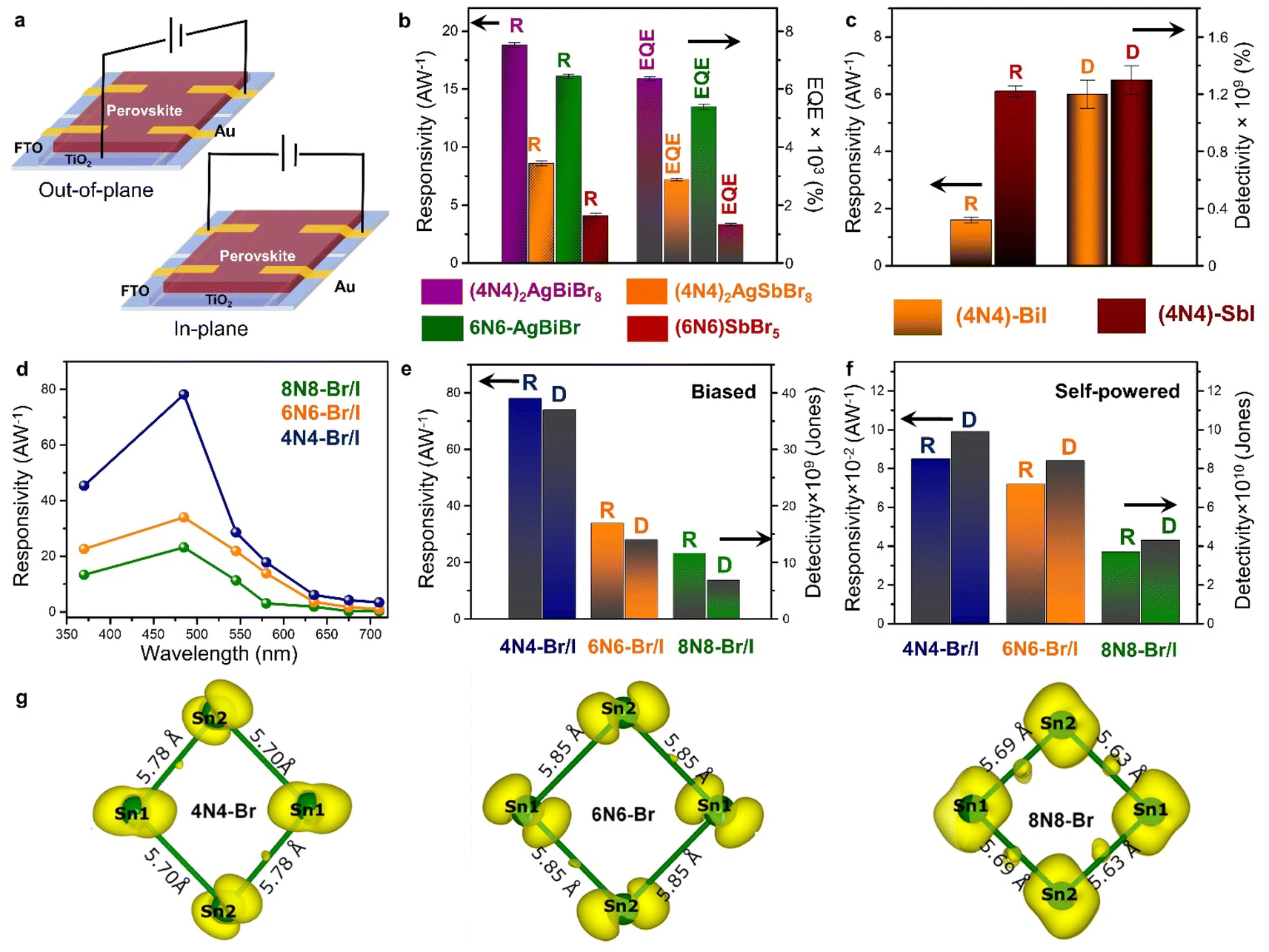 | ||
| Fig. 7 (a) Schematic demonstration of the out-of-plane and in-plane photodetector devices. Statistical bar diagrams of (b) R and EQE (%) of the HLDP structures, and (c) R and D of 1D 4N4-BiI, and 4N4-SbI.11 (d) Wavelength dependant variation of R, and statistical bar diagram of R and D under (e) potential-biased, and (f) self-powered conditions for the DJ (xNx)Sn(Br/I)4 (x = 8N8, 6N6, 4N4).23 (g) The spatially resolved charge density corresponding to the CBM of 4N4-Br, 6N6-Br, and 8N8-Br. The bond lengths of the inorganic network formed by the Sn atoms are also shown.23 Reproduced with permission from ref. 11, copyright (2023) Royal Society of Chemistry, and ref. 23, copyright (2023) American Chemical Society of Chemistry. | ||
Photodetectors of HLDPs
The HLDPs exhibit an appreciable wavelength-dependent photodetection in terms of the parameters such as responsivity (R), detectivity (D), and EQE, at a certain applied voltage (Fig. 7b and c).11 While the 2D arrangement of the inorganic octahedra allows a facile flow of the photo-generated charge carriers, the 1D hybrid halides constrict the mobility. The carrier flow is even more restricted in the 0D perovskite dimers such as Cs3M2I9 (M = Bi3+, Sb3+) having disconnected inorganic units.103,104 The ambient-stable Bi3+ and Sb3+ containing HLDPs can be used as self-powered photodetectors because of the favourable juxtaposition of the VBM and CBM with the ETL, and fermi energy of the metal contact. Moreso, the electronic communication can be substantially increased by lowering the separation between the inorganic layers. As shown in Fig. 7b, (4N4)2AgBiBr8 with a lower separation across the 4-C spacer shows greater values of R and EQE than the 6N6 counterpart.11 (4N4)2AgBiBr8 shows a R of 18.8 ± 0.2 A W−1, and EQE of 6360 ± 58% at 2.5 V, under 370 nm (27 mW cm−2) illumination. In self-powered mode, (4N4)2AgBiBr8 has the maximum R of 0.67, and 0.36 mA W−1 under 370 nm, and visible light illumination. Additionally, the Sb-based hybrid halides with higher optical band gaps, show lower photodetection ability than the Bi hybrids (Fig. 7b). Under similar illumination, (4N4)2AgSbBr8 has a R of 8.6 ± 0.2 AW−1, and EQE of 2880 ± 58% at 2 V. The 1D hybrid halides, (4N4)-BiI and (4N4)-SbI, show wavelength dependent photoresponse. In the self-powered mode, (4N4)-SbI has a better R of 11.7 mA W−1 under 485 nm illumination.Impact of halide composition in 2D Sn-perovskite photodetectors
The variation in chain length of the organic spacer cations manifests an attenuation of the QW barrier of the layered halide perovskites that alters the photodetection under potential bias, and self-powered conditions. A decrease in the spacer layer thickness from 8N8 to 4N4, decreases the interplanar distance (Λ), and therefore increases the Δ2θ interval of the equidistant (00l) reflections.23 The halide composition also has a tremendous impact on the optoelectronic performance. Although the iodide perovskites exhibit lower optical band gap, increasing the iodide content aggravates the issue of halide ion migration. As a result, the contrasting effect of halide ions and spacer chain lengths is reflected in the photodetection property of the out-of-plane devices. The mixed halide (8N8)SnBr2I2 (8N8-Br/I) has lower band gap than (8N8)SnBr4 (8N8-Br), and better phase purity than (8N8)SnI4 (8N8-I). Incorporating the iodide extends the photodetection in the wide spectral range. All the devices show wavelength and intensity-dependent photodetection under applied potential bias, and self-powered conditions. Since the photodetection parameters are inversely proportional to the illumination intensity (Llight), the maximum R, D, and EQE are obtained when Llight is much reduced at 485 nm.23 In contrast, since 8N8-Br has optical absorption in the near UV region, the best photodetector performance is obtained at 370 nm. 8N8-Br/I has a R of 23.2 A W−1, and EQE of 5930% at 3 V under 485 nm illumination. A facile charge transfer, reduced charge trapping, and halide migration escalate the device photoresponse.Impact of spacer layer thickness on photodetection
Since, the organic ammonium cation plays an important role in deciding the optoelectronic properties of the layered halide perovskite, its impact on the electronic and structural characteristics of the perovskite should be adjudged, along with its effect on the film quality. If the film quality, and roughness of the films are not altered significantly, the trend in the extent of charge transfer is majorly guided by the intrinsic factors. Maintaining the same composition in the inorganic framework, the layered halide perovskite with a shorter spacer thickness is expected to deliver better performance, due to lower interlayer separation between the inorganic units. The photodetectors with the shorter spacer (4N4-Br/I), therefore display higher current densities as a function of the applied potential (0–3 V) under an illumination of 100 mW cm−2.23 A maximum R of 78.1 AW−1 has been obtained for 4N4-Br/I at 485 nm under 3 V potential bias, much better than 6N6-Br/I, and 8N8-Br/I (Fig. 7d and e). The Sn-based mixed halide DJ perovskites also exhibit remarkable self-powered photodetection, where the maximum R and D for 4N4-Br/I are 0.085 AW−1, and 9.9 × 10¹⁰ Jones, respectively (Fig. 7f).23 The minimized dark current density (JD) reinforces the D value in the absence of any potential bias.A sustained current density (JL) under constant illumination can be validated from the chronoamperometry plots. With increasing light intensity, the current densities of the 4N4-Br/I self-powered devices increase up to a threshold point followed by a lowering of the current density. An intense illumination induces ion migration, and halide segregation leading to the degradation of the films. In contrast, the increased hydrophobic thickness in 6N6-Br/I, and 8N8-Br/I prevents the film degradation, despite having a lower JL as compared to the 4N4-Br/I films.23 The reduced rise time (RT) and fall time (FT), obtained from the chronoamperometry plots imply a fast photoresponse under the self-powered condition for the 4N4-Br/I films.
A lower charge transfer resistance, higher hole mobility, and improved lifetime of the charge carriers, further emphasizes the advantage of a shorter spacer thickness in employing the layered halide perovskites in optoelectronic devices. A comparison between the DJ, and RP analogues of the Sn-based layered halide perovskites show that the DJ phases experience a relatively lower Eb, and higher extent of charge extraction. On the other hand, the van der Waals gap in between the organic bilayer of the RP phase reduces the charge extraction, and carrier mobility, resulting in a subservient photodetection capability. As compared to the DJ 8N8-Br/I, the (8N)2SnBr2I2 (8N-RP-Br/I) RP phase shows a subdued R value of 4.4 AW−1, and EQE of 1120% at 3 V under 485 nm illumination.23
Role of descriptors
Generally, the high absorption coefficient of low band gap semiconductors is considered a favourable attribute for the photodetectors. In most cases, the optoelectronic descriptors namely, the band gap, effective mass, out-of-plane mobility, transition probability of band edge transition, and net volume of the perovskites can explain the optoelectronic trend as a function of spacer layer thickness.9,11 In rare instances, the spin orientation at the VBM and CBM play a pivotal role in deciding the direct vs. indirect optical transitions.23 In halide perovskites, structural distortions, and heavy elements create substantial spin–orbit interactions which lead to the spin texture in the VBM and CBM, despite the absence of any intrinsic magnetic property. Increasing spacer layer thickness can mould the spin–orbit coupling which modifies the wave function at the CBM and VBM, resulting in significant differences in their spin orientations. For example, the individual p-orbital contributions at the CBM are altered due to the admixture of the py orbital with the px orbital for the labelled Sn1 atom in 6N6-Br and 8N8-Br systems that arise from the structural distortions (Fig. 6e and 7g). Since the Sn p-orbital is not pointed towards the anion site, such a complex spin texture is observed which results in the direct and indirect transition probability with varying spacer chain length. The probability of direct transition increases from 8N8 to 4N4 systems. Due to the absence of any py orbital admixture at the CBM of 4N4-Br/I, the photodetection parameters are enhanced with the shortest 4N4 system. In case of 4N4-Br/I, the direct component is more than 95% at Sn1 and Sn2 centers, whereas for 8N8-Br/I, it decreases to ∼74%.23 However, the major descriptor that can explain the trend of optoelectronics depends on the architecture of the layered halide perovskite lattice, wherein theoretical calculations, in combination with the experimental results, can resolve the paradox.Conclusions and perspective
Despite the toxic Pb-containing perovskites having achieved significant milestones in photovoltaics over the past decade, this perspective highlights the immense potential of lead-free alternatives in optoelectronics. Both Pb- and Sn-based hybrid perovskites exhibit favourable characteristics such as a decent band gap, strong absorption, low effective mass, and high mobility of the charge carriers, rendering them promising for various device applications. The Sn-center possesses a unique advantage in the form of active ns2 configuration with lesser inert pair effect than the Pb2+ 6s orbital. This allows a facile interaction with the surrounding ligands, enabling the moulding of the perovskite lattice, and structural dimensions.In addition to the low-dimensional hybrid halides, HLDP phases, and vacancy ordered double perovskites, this perspective is particularly focused on the RP and DJ phases of Sn2+-containing layered halide perovskite single crystals and NPL superlattices. Beyond the single crystals, and depending on the LARP or HI synthesis, the inorganic octahedral layers can assemble into periodically stacked NPLs, cojoined by the organic amine, giving rise to a superlattice or superstructure. The synthesis of single crystals and nanostructures of layered halide perovskites relies on regulating thermodynamic parameters and the solubility of active precursors in the solution, yet there are nuanced differences in stabilizing each. Firstly, a high temperature is initially required to dissolve all the precursors, followed by cooling to a lower temperature for preparing the single crystals by acid precipitation. To synthesize the anisotropic layered nanostructures by HI method, high temperatures are disadvantageous, as they facilitate overcoming the activation energy needed for isotropic growth of the nanoparticles, rather than the desired anisotropic growth. Secondly, the nanostructures exhibit a preference for long-chain hydrophobic amines, such as oleylamine, to stabilize the periodic array of the NPLs. Conversely, the layered halide perovskite single crystals favour spacer amines with moderate chain lengths. Third, the single crystals can achieve the stabilization of n = 1 phase, whereas, synthesizing pure n = 1 phase layered nanostructures via the HI method in the Schlenk line is a considerable challenge. Fourth, the introduction of a foreign metal center in the parent structure presents another synthetic challenge. Single crystals exhibit resistance to alloying within the lattice structure of the layered halide perovskites. In contrast, the nanostructures are more receptive for incorporating the foreign metals into their lattice. However, this process requires a substantial stimulus, since a greater amount of foreign metal precursor is needed to infiltrate the lattice.
The optical properties of the layered halide perovskites are a function of the organic spacer layer thickness, the metal center, and the halide composition. In most cases, the distinct absorption and PL features have their origin in the STE emission guided by the structural deformation, octahedral tilting, and the polaronic effect. The STE emission-guided PLQY is more prominent in the presence of longer spacer cations. Even though the layered halide perovskite single crystals often exhibit a high PLQY, the assembled nanostructures demonstrate superfluorescence, also characterized by a high PLQY.
The layered halide perovskites hold substantial promise for LED applications due to their tuneable quantum confinement effect and high PLQY compared to their 3D counterparts. However, their potential in solar cells, and FETs is limited due to the presence of hydrophobic organic chains, which can hinder carrier mobility and the charge extraction process. In this context, the research on 3D/2D heterojunction solar cells has gained attention in the recent years. While these layered halide structures excel in LED applications, their suitability for commercial displays and laser applications is hindered by the presence of multiple emission peaks for n > 1 phases, which compromises their phase, and colour purity. The long-term thermal and optical stability of single crystals, nanostructures, and devices in ambient atmospheric conditions poses another significant hurdle to the commercialization of these materials across various applications.
The extent of their optoelectronic performance is attuned by the excitonic band gap, dielectric constant, effective mass, carrier mobility, Rashba splitting, as well as the spin texture at the VBM and CBM. The shortest spacer chain length of the organic ammonium cation has so far demonstrated the most promising photodetector performance. In addition to the intrinsic descriptors, the optoelectronic performance relies on the quality of the photoactive layer, whether it's in the form of single crystals or polycrystalline films. While preparing large-area single crystals poses challenges due to their fragile and brittle nature, creating the pinhole-free and homogeneous polycrystalline films presents even greater difficulties. Single crystals are often synthesized in an acid solution, while organic solvents are typically used for film preparation via the spin-coating method. The thermodynamic and kinetic processes involved in the crystallization and growth of layered halide perovskite films are fundamentally distinct from those governing the growth of single crystals. To understand the effects of the spacer on device efficiency, a thorough analysis encompassing the growth mechanism, crystallinity, morphology, orientation, precise composition, interactions in multiple phases, phase selectivity, and stability of the film is essential.
To conclude, 2D halide perovskites offer ample opportunities ranging from single crystals to 2D superlattices, equipped with a rich and diverse variety of optical and optoelectronic properties. Beyond the photodetectors or solar cells, the lead-free layered halide perovskites exhibit diverse applications such as X-ray detectors, ferro- and antiferroelectric materials, and anticounterfeiting agents, showcasing their versatility and potential across various technological domains. On the other hand, in the relatively new area of NPL superlattices, despite some focus on structural details, the potential of these long-range periodicity remains largely untapped in optoelectronics and photovoltaics, presenting a promising avenue for further exploration. Given the potential for a range of structural analogues, 2D halide perovskites hold promise for the advancement of modern electronics and next-generation renewable energy solutions.
Author contributions
V. H., A. M. and S. B. conceptualized the idea, and co-wrote the perspective; S. B. supervised the entire project.Conflicts of interest
There are no conflicts to declare.Acknowledgements
V. H. and A. M. thank the University Grants Commission (UGC), New Delhi, for their fellowships. S. B. thanks the financial support from SERB under Sanction No. CRG/2020/000084 and STR/2021/000001.References
- L. Chouhan, S. Ghimire, C. Subrahmanyam, T. Miyasaka and V. Biju, Chem. Soc. Rev., 2020, 49, 2869–2885 RSC.
- Y. Zou, T. Zou, C. Zhao, B. Wang, J. Xing, Z. Yu, J. Cheng, W. Xin, J. Yang, W. Yu, H. Dong and C. Guo, Small, 2020, 16, 2000733 CrossRef CAS PubMed.
- A. Mandal, A. Ghosh, S. P. Senanayak, R. H. Friend and S. Bhattacharyya, J. Phys. Chem. Lett., 2021, 12, 1560–1566 CrossRef CAS PubMed.
- NREL, Best Research-Cell Efficiency Chart, Photovoltaic Research, NREL, 2022, https://www.nrel.gov/pv/cellefficiency.html Search PubMed.
- C. Zheng and O. Rubel, J. Phys. Chem. C, 2019, 123, 19385–19394 CrossRef CAS.
- A. F. Akbulatov, M. I. Ustinova, G. V. Shilov, N. N. Dremova, I. S. Zhidkov, E. Z. Kurmaev, L. A. Frolova, A. F. Shestakov, S. M. Aldoshin and P. A. Troshin, J. Phys. Chem. Lett., 2021, 12, 4362–4367 CrossRef CAS PubMed.
- H. Lei, D. Hardy and F. Gao, Adv. Funct. Mater., 2021, 31, 2105898 CrossRef CAS.
- W. Li, X. Wang, J. Liao, Y. Jiang and D. Kuang, Adv. Funct. Mater., 2020, 30, 1909701 CrossRef CAS.
- A. Mandal, S. Roy, A. Mondal, S. Gupta, B. Pal and S. Bhattacharyya, J. Phys. Chem. Lett., 2022, 13, 9103–9113 CrossRef CAS PubMed.
- X. Li, J. M. Hoffman and M. G. Kanatzidis, Chem. Rev., 2021, 121, 2230–2291 CrossRef CAS PubMed.
- A. Mandal, S. Gupta, S. Dutta, S. K. Pati and S. Bhattacharyya, Chem. Sci., 2023, 14, 9770–9779 RSC.
- H. Yu, Y. Xie, J. Zhang, J. Duan, X. Chen, Y. Liang, K. Wang and L. Xu, Adv. Sci., 2021, 8, 2004510 CrossRef CAS.
- J. Cho, J. T. DuBose, A. N. Le and P. V. Kamat, ACS Mater. Lett., 2020, 2, 565–570 CrossRef CAS.
- Y. Yuan and J. Huang, Acc. Chem. Res., 2016, 49, 286–293 CrossRef CAS PubMed.
- Y. Zhang, P. Wang, M.-C. Tang, D. Barrit, W. Ke, J. Liu, T. Luo, Y. Liu, T. Niu, D.-M. Smilgies, Z. Yang, Z. Liu, S. Jin, M. G. Kanatzidis, A. Amassian, S. F. Liu and K. Zhao, J. Am. Chem. Soc., 2019, 141, 2684–2694 CrossRef CAS PubMed.
- G. Park, I.-H. Oh, J. M. Park, J. Jung, C.-Y. You, J.-S. Kim, Y. Kim, J. H. Jung, N. Hur, Y. Kim, J.-Y. Kim, C. S. Hong and K.-Y. Kim, Sci. Rep., 2018, 8, 4661 CrossRef.
- S. Toso, D. Baranov, U. Filippi, C. Giannini and L. Manna, Acc. Chem. Res., 2022, 56, 66–76 CrossRef PubMed.
- S. Bera, R. K. Behera and N. Pradhan, J. Am. Chem. Soc., 2020, 142, 20865–20874 CrossRef CAS PubMed.
- E. Mahal, D. Roy, S. S. Manna and B. Pathak, J. Mater. Chem. A, 2023, 11, 23547–23555 RSC.
- L. Zhang, X. Zhang and G. Lu, J. Phys. Chem. Lett., 2020, 11, 2910–2916 CrossRef CAS PubMed.
- M. P. Hautzinger, D. Pan, A. K. Pigg, Y. Fu, D. J. Morrow, M. Leng, M.-Y. Kuo, N. Spitha, D. P. Lafayette, D. D. Kohler, J. C. Wright and S. Jin, ACS Energy Lett., 2020, 5, 1430–1437 CrossRef CAS.
- R. Prasanna, A. Gold-Parker, T. Leijtens, B. Conings, A. Babayigit, H.-G. Boyen, M. F. Toney and M. D. McGehee, J. Am. Chem. Soc., 2017, 139, 11117–11124 CrossRef CAS PubMed.
- A. Mandal, S. K. Khuntia, D. Mondal, P. Mahadevan and S. Bhattacharyya, J. Am. Chem. Soc., 2023, 145, 24990–25002 CrossRef CAS.
- D. Ghosh, D. K. Chaudhary, M. Y. Ali, K. K. Chauhan, S. Prodhan, S. Bhattacharya, B. Ghosh, P. K. Datta, S. C. Ray and S. Bhattacharyya, Chem. Sci., 2019, 10, 9530–9541 RSC.
- B. Chen, R. Yu, G. Xing, Y. Wang, W. Wang, Y. Chen, X. Xu and Q. Zhao, ACS Energy Lett., 2024, 9, 226–242 CrossRef CAS.
- M. D. Smith, L. Pedesseau, M. Kepenekian, I. C. Smith, C. Katan, J. Even and H. I. Karunadasa, Chem. Sci., 2017, 8, 1960–1968 RSC.
- K. Marjit, A. G. Francis, S. K. Pati and A. Patra, J. Phys. Chem. C, 2023, 14, 10900–10909 CAS.
- R. Chakraborty and A. Nag, Phys. Chem. Chem. Phys., 2021, 23, 82–93 RSC.
- M. Wuttig, C. Schön, M. Schumacher, J. Robertson, P. Golub, E. Bousquet, C. Gatti and J. Raty, Adv. Funct. Mater., 2021, 32, 2110166 CrossRef.
- M. Dyksik, H. Duim, X. Zhu, Z. Yang, M. Gen, Y. Kohama, S. Adjokatse, D. K. Maude, M. A. Loi, D. A. Egger, M. Baranowski and P. Plochocka, ACS Energy Lett., 2020, 5, 3609–3616 CrossRef CAS.
- M. Michiardi, F. Boschini, H.-H. Kung, M. X. Na, S. K. Dufresne, A. Currie, G. Levy, S. Zhdanovich, A. K. Mills, D. J. Jones, J. L. Mi, B. B. Iversen, Ph. Hofmann and A. Damascelli, Nat. Commun., 2022, 13, 3096 CrossRef CAS PubMed.
- S. McKechnie, J. M. Frost, D. Pashov, P. Azarhoosh, A. Walsh and M. van Schilfgaarde, Phys. Rev. B, 2018, 98, 085108 CrossRef CAS.
- E. Mosconi, T. Etienne and F. De Angelis, J. Phys. Chem. Lett., 2017, 8, 2247–2252 CrossRef CAS PubMed.
- E. Lafalce, E. Amerling, Z.-G. Yu, P. C. Sercel, L. Whittaker-Brooks and Z. V. Vardeny, Nat. Commun., 2022, 13, 483 CrossRef CAS PubMed.
- Y. Zhai, S. Baniya, C. Zhang, J. Li, P. Haney, C.-X. Sheng, E. Ehrenfreund and Z. V. Vardeny, Sci. Adv., 2017, 3, 1700704 CrossRef.
- N. Zibouche and M. S. Islam, ACS Appl. Mater. Interfaces, 2020, 12, 15328–15337 CrossRef CAS PubMed.
- J. Yin, P. Maity, L. Xu, A. M. El-Zohry, H. Li, O. M. Bakr, J.-L. Brédas and O. F. Mohammed, Chem. Mater., 2018, 30, 8538–8545 CrossRef CAS.
- J. K. Pious, M. G. Basavarajappa, C. Muthu, R. Nishikubo, A. Saeki, S. Chakraborty, A. Takai, M. Takeuchi and C. Vijayakumar, J. Phys. Chem. Lett., 2021, 12, 5758–5764 CrossRef CAS PubMed.
- M. Isarov, L. Z. Tan, M. I. Bodnarchuk, M. V. Kovalenko, A. M. Rappe and E. Lifshitz, Nano Lett., 2017, 17, 5020–5026 CrossRef CAS PubMed.
- S. D. Stranks and P. Plochocka, Nat. Mater., 2018, 17, 381–382 CrossRef CAS PubMed.
- E. M. Hutter and T. J. Savenije, ACS Energy Lett., 2018, 3, 2068–2069 CrossRef CAS PubMed.
- L. Mao, J. Chen, P. Vishnoi and A. K. Cheetham, Acc. Mater. Res., 2022, 3, 439–448 CrossRef CAS.
- J. Li, Y. Sang, L. Xu, H. Lu, J. Wang and Z. Chen, Angew. Chem., Int. Ed., 2021, 61, 202113450 CrossRef.
- H. Fattal, T. D. Creason, C. J. Delzer, A. Yangui, J. P. Hayward, B. J. Ross, M.-H. Du, D. T. Glatzhofer and B. Saparov, Inorg. Chem., 2021, 60, 1045–1054 CrossRef CAS.
- J. K. Pious, C. Muthu and C. Vijayakumar, Acc. Chem. Res., 2021, 55, 275–285 CrossRef PubMed.
- J. K. Pious, M. G. Basavarajappa, C. Muthu, N. Krishna, R. Nishikubo, A. Saeki, S. Chakraborty and C. Vijayakumar, J. Phys. Chem. Lett., 2020, 11, 6757–6762 CrossRef CAS PubMed.
- W. Zhang, X. Liu, L. Li, Z. Sun, S. Han, Z. Wu and J. Luo, Chem. Mater., 2018, 30, 4081–4088 CrossRef CAS.
- I. W. Oswald, E. M. Mozur, I. P. Moseley, H. Ahn and J. R. Neilson, Inorg. Chem., 2019, 58, 5818–5826 CrossRef CAS PubMed.
- J. K. Pious, C. Muthu, S. Dani, A. Saeki and C. Vijayakumar, Chem. Mater., 2020, 32, 2647–2652 CrossRef CAS.
- M.-Q. Li, Y.-Q. Hu, L.-Y. Bi, H.-L. Zhang, Y. Wang and Y.-Z. Zheng, Chem. Mater., 2017, 29, 5463–5467 CrossRef CAS.
- D. B. Mitzi, Inorg. Chem., 2000, 39, 6107–6113 CrossRef CAS PubMed.
- S. Zhou, Y. Chen, K. Li, X. Liu, T. Zhang, W. Shen, M. Li, L. Zhou and R. He, Chem. Sci., 2023, 14, 5415–5424 RSC.
- D. Liang, H. Xiao, W. Cai, S. Lu, S. Zhao, Z. Zang and L. Xie, Adv. Opt. Mater., 2023, 11, 2202997 CrossRef CAS.
- J. K. Pious, A. Katre, C. Muthu, S. Chakraborty, S. Krishna and C. Vijayakumar, Chem. Mater., 2019, 31, 1941–1945 CrossRef CAS.
- D. B. Mitzi, S. Wang, C. A. Feild, C. A. Chess and A. M. Guloy, Science, 1995, 267, 1473–1476 CrossRef CAS.
- P. Huang, S. Kazim, M. Wang and S. Ahmad, ACS Energy Lett., 2019, 4, 2960–2974 CrossRef CAS.
- D. B. Mitzi, D. R. Medeiros and P. R. Malenfant, Inorg. Chem., 2002, 41, 2134–2145 CrossRef CAS PubMed.
- T. Sheikh, V. Nawale, N. Pathoor, C. Phadnis, A. Chowdhury and A. Nag, Angew. Chem., Int. Ed., 2020, 59, 11653–11659 CrossRef CAS.
- T. Zhang, C. Zhou, X. Feng, N. Dong, H. Chen, X. Chen, L. Zhang, J. Lin and J. Wang, Nat. Commun., 2022, 13, 60 CrossRef CAS.
- S. Wang, J. Popović, S. Burazer, A. Portniagin, F. Liu, K. Low, Z. Duan, Y. Li, Y. Xiong, Y. Zhu, S. V. Kershaw, A. B. Djurišić and A. L. Rogach, Adv. Funct. Mater., 2021, 31, 2102182 CrossRef CAS.
- S. Neutzner, F. Thouin, D. Cortecchia, A. Petrozza, C. Silva and A. R. S. Kandada, Phys. Rev. Mater., 2018, 2, 064605 CrossRef CAS.
- R. Biega, Y. Chen, M. R. Filip and L. Leppert, Nano Lett., 2023, 23, 8155–8161 CrossRef CAS.
- M. D. Smith and H. I. Karunadasa, Acc. Chem. Res., 2018, 51, 619–627 CrossRef CAS PubMed.
- T. Hu, M. D. Smith, E. R. Dohner, M.-J. Sher, X. Wu, M. T. Trinh, A. Fisher, J. Corbett, X.-Y. Zhu, H. I. Karunadasa and A. M. Lindenberg, Phys. Chem. Lett., 2016, 7, 2258–2263 CrossRef CAS.
- S. Kahmann, E. K. Tekelenburg, H. Duim, M. E. Kamminga and M. A. Loi, Nat. Commun., 2020, 11, 2344 CrossRef CAS PubMed.
- H. Yang, S. Mandal, Y. H. Lee, J. Y. Park, H. Zhao, C. Yuan, L. Huang, M. Chen and L. Dou, J. Am. Chem. Soc., 2023, 145, 23963–23971 CrossRef CAS PubMed.
- Q. A. Akkerman and L. Manna, ACS Energy Lett., 2020, 5, 604–611 CrossRef CAS PubMed.
- G. Ji and Z. Xiao, Chem. Mater., 2022, 34, 8207–8212 CrossRef CAS.
- L. Lian, X. Wang, P. Zhang, J. Zhu, X. Zhang, J. Gao, S. Wang, G. Liang, D. Zhang, L. Gao, H. Song, R. Chen, X. Lan, W. Liang, G. Niu, J. Tang and J. Zhang, J. Phys. Chem. Lett., 2021, 12, 6919–6926 CrossRef CAS PubMed.
- D. Banerjee and B. Saparov, Chem. Mater., 2023, 35, 3364–3385 CrossRef CAS.
- L.-K. Gong, Q.-Q. Hu, F.-Q. Huang, Z.-Z. Zhang, N.-N. Shen, B. Hu, Y. Song, Z.-P. Wang, K.-Z. Du and X.-Y. Huang, Chem. Commun., 2019, 55, 7303–7306 RSC.
- F. Jiang, Z. Wu, M. Lu, Y. Gao, X. Li, X. Bai, Y. Ji and Y. Zhang, Adv. Mater., 2023, 35, 2211088 CrossRef CAS PubMed.
- C. Yang, Q. Wei, Y. Gong, M. Long, G. Zhou, G. Xing and B. Wu, J. Phys. Chem. Lett., 2023, 14, 10046–10053 CrossRef CAS PubMed.
- C. Franchini, M. Reticcioli, M. Setvin and U. Diebold, Nat. Rev. Mater., 2021, 6, 560–586 CrossRef CAS.
- A. L. Shluger and A. M. Stoneham, J. Condens. Matter Phys., 1993, 5, 3049–3086 CrossRef CAS.
- Y. Yamada and Y. Kanemitsu, NPG Asia Mater., 2022, 14, 48 CrossRef CAS.
- H. Ruan, Z. Guo, J. Lin, K. Liu, L. Guo, X. Chen, J. Zhao, Q. Liu and W. Yuan, Inorg. Chem., 2021, 60, 14629–14635 CrossRef CAS PubMed.
- P. Vishnoi, J. L. Zuo, X. Li, D. C. Binwal, K. E. Wyckoff, L. Mao, L. Kautzsch, G. Wu, S. D. Wilson, M. G. Kanatzidis, R. Seshadri and A. K. Cheetham, J. Am. Chem. Soc., 2022, 144, 6661–6666 CrossRef CAS.
- J. Xue, Z. Wang, A. Comstock, Z. Wang, H. H. Sung, I. D. Williams, D. Sun, J. Liu and H. Lu, Chem. Mater., 2022, 34, 2813–2823 CrossRef CAS.
- M. K. Jana, S. M. Janke, D. J. Dirkes, S. Dovletgeldi, C. Liu, X. Qin, K. Gundogdu, W. You, V. Blum and D. B. Mitzi, J. Am. Chem. Soc., 2019, 141, 7955–7964 CrossRef CAS PubMed.
- D. Li, X. Liu, W. Wu, Y. Peng, S. Zhao, L. Li, M. Hong and J. Luo, Angew. Chem., Int. Ed., 2021, 133, 8496–8499 CrossRef.
- B. Vargas, E. Ramos, E. Pérez-Gutiérrez, J. C. Alonso and D. Solis-Ibarra, J. Am. Chem. Soc., 2017, 139, 9116–9119 CrossRef CAS.
- H. Yang, W. Shi, T. Cai, K. Hills-Kimball, Z. Liu, L. Dube and O. Chen, Nanoscale, 2020, 12, 23191–23199 RSC.
- B. Vargas, E. Coutiño-Gonzalez, O. Ovalle-Encinia, C. Sánchez-Aké and D. Solis-Ibarra, J. Phys. Chem. Lett., 2020, 11, 10362–10367 CrossRef CAS PubMed.
- M. C. Folgueras, Y. Jiang, J. Jin and P. Yang, Nature, 2023, 621, 282–288 CrossRef CAS.
- P. Fu, M. A. Quintero, E. S. Vasileiadou, P. Raval, C. Welton, M. Kepenekian, G. Volonakis, J. Even, Y. Liu, C. Malliakas, Y. Yang, C. Laing, V. P. Dravid, G. N. Reddy, C. Li, E. H. Sargent and M. G. Kanatzidis, J. Am. Chem. Soc., 2023, 145, 15997–16014 CrossRef CAS PubMed.
- A. N. Yadav, S. Min, H. Choe, J. Park and J. Cho, Small, 2023, 20, 2305546 CrossRef PubMed.
- E. H. Massasa, R. Strassberg, R. Shechter, S. Dror, S. Khalfin, S. Shaek, M. K. Khristosov, I. Hadar and Y. Bekenstein, Adv. Funct. Mater., 2023, 34, 2311122 CrossRef.
- V. Hazra, S. Mondal, P. Pattanayak and S. Bhattacharyya, Small, 2024, 20, 2304920 CrossRef CAS.
- J. Jagielski, S. F. Solari, L. Jordan, D. Scullion, B. Blülle, Y.-T. Li, F. Krumeich, Y.-C. Chiu, B. Ruhstaller, E. J. Santos and C.-J. Shih, Nat. Commun., 2020, 11, 387 CrossRef CAS PubMed.
- A. K. Poonia, B. Mondal, M. C. Beard, A. Nag and K. V. Adarsh, Phys. Rev. Lett., 2024, 132, 063803 CrossRef CAS.
- A. Mandal, V. Hazra and S. Bhattacharyya, J. Phys. Chem. C, 2023, 127, 11767–11779 CrossRef CAS.
- A. Mandal, A. Ghosh, D. Ghosh and S. Bhattacharyya, ACS Appl. Mater. Interfaces, 2021, 13, 43104–43114 CrossRef CAS.
- N. Liu, P. Liu, H. Zhou, Y. Bai and Q. Chen, J. Phys. Chem. Lett., 2020, 11, 3521–3528 CrossRef CAS PubMed.
- G. Walters, L. Haeberlé, R. Quintero-Bermudez, J. Brodeur, S. Kéna-Cohen and E. H. Sargent, J. Phys. Chem. Lett., 2020, 11, 3458–3465 CrossRef CAS PubMed.
- F. Li, W. Yu, X. Guan and T. Wu, Acc. Mater. Res., 2021, 3, 8–20 CrossRef.
- Y. Shen, C. Ran, X. Dong, Z. Wu and W. Huang, Small, 2023, 2308242 Search PubMed.
- L. Li, S. Ye, J. Qu, F. Zhou, J. Song and G. Shen, Small, 2021, 17, 2005606 CrossRef CAS.
- Z. Wang, F. Wang, B. Zhao, S. Qu, T. Hayat, A. Alsaedi, L. Sui, K. Yuan, J. Zhang, Z. Wei and Z. Tan, J. Phys. Chem. Lett., 2020, 11, 1120–1127 CrossRef CAS PubMed.
- G. Vescio, J. Sanchez-Diaz, J. L. Frieiro, R. S. Sánchez, S. Hernández, A. Cirera, I. Mora-Seró and B. Garrido, ACS Energy Lett., 2022, 7, 3653–3655 CrossRef CAS PubMed.
- T. Matsushima, S. Hwang, A. S. Sandanayaka, C. Qin, S. Terakawa, T. Fujihara, M. Yahiro and C. Adachi, Adv. Mater., 2016, 28, 10275–10281 CrossRef CAS PubMed.
- Y. Gao, Z. Wei, P. Yoo, E. Shi, M. Zeller, C. Zhu, P. Liao and L. Dou, J. Am. Chem. Soc., 2019, 141, 15577–15585 CrossRef CAS.
- S. Devasia, S. Shaji, D. A. Avellaneda, J. A. Aguilar Martinez and B. Krishnan, Mater. Chem. Phys., 2023, 296, 127295 CrossRef CAS.
- J. Mei, M. Liu, P. Vivo and V. Pecunia, Adv. Funct. Mater., 2021, 31, 2106295 CrossRef CAS.
| This journal is © The Royal Society of Chemistry 2024 |