
 Open Access Article
 This Open Access Article is licensed under a Creative Commons Attribution-Non Commercial 3.0 Unported Licence
Construction of nanoparticle-on-mirror nanocavities and their applications in plasmon-enhanced spectroscopy
Wei
Peng
a,
Jing-Wen
Zhou
a,
Mu-Lin
Li
a,
Lan
Sun
 a,
Yue-Jiao
Zhang
*a and
Jian-Feng
Li
*ab
a,
Yue-Jiao
Zhang
*a and
Jian-Feng
Li
*ab
aCollege of Energy, State Key Laboratory of Physical Chemistry of Solid Surfaces, iChEM, College of Chemistry and Chemical Engineering, Xiamen University, Xiamen 361005, China. E-mail: zhangyuejiao@xmu.edu.cn; Li@xmu.edu.cn
bCollege of Chemistry, Chemical Engineering and Environment, Minnan Normal University, Zhangzhou 363000, China
First published on 16th January 2024
Abstract
Plasmonic nanocavities exhibit exceptional capabilities in visualizing the internal structure of a single molecule at sub-nanometer resolution. Among these, an easily manufacturable nanoparticle-on-mirror (NPoM) nanocavity is a successful and powerful platform for demonstrating various optical phenomena. Exciting advances in surface-enhanced spectroscopy using NPoM nanocavities have been developed and explored, including enhanced Raman, fluorescence, phosphorescence, upconversion, etc. This perspective emphasizes the construction of NPoM nanocavities and their applications in achieving higher enhancement capabilities or spatial resolution in dark-field scattering spectroscopy and plasmon-enhanced spectroscopy. We describe a systematic framework that elucidates how to meet the requirements for studying light–matter interactions through the creation of well-designed NPoM nanocavities. Additionally, it provides an outlook on the challenges, future development directions, and practical applications in the field of plasmon-enhanced spectroscopy.
1. Introduction
When metal nanoparticles (NPs) or nanostructures are exposed to incident light with specific wavelengths, the electrons in the metal conduction band begin to oscillate collectively.1,2 This oscillation of surface free electrons generates highly localized electromagnetic fields around the nanostructures, giving rise to a phenomenon widely known as localized surface plasmon resonance (LSPR).3,4 These excited plasmonic nanoparticles or structures can be treated as antennas, effectively amplifying the intensity of the optical field in their immediate vicinity.5,6 The strength of the electric field decreases with distance from the particle surface, following a decay rate of r3, where ‘r’ represents the distance from the metal surface. As a result, molecules situated on or near the nanostructure surface can experience an enhanced optical field, leading to the enhancement or modification of various optical processes.7–9 The optical processes based on LSPR that have been developed and are gradually being applied primarily encompass: (1) enhanced scattering processes, such as surface-enhanced Raman spectroscopy (SERS);10–12 (2) enhanced radiative processes, including photoluminescence (PL) (surface-enhanced fluorescence (SEF),5,13,14 enhanced phosphorescence (SEP), and enhanced upconversion),15,16 electroluminescence (ECL),17 and chemiluminescence (CL);18 (3) enhanced absorption processes, such as enhanced infrared (IR).19The resonance characteristics of LSPR are closely associated with various factors, including the inherent properties of metal nanoparticles, their composition, particle morphology, size, and surrounding environment.20,21 (1) The intrinsic properties and composition of the materials play a significant role. These factors encompass aspects such as the presence of free electrons, carrier concentration, carrier mobility, and carrier impedance on the metal surface. Typically, materials like Au, Ag, and Cu are the most employed. Among them, Au is the most stable under ambient conditions but relatively costly. Ag exhibits the lowest dielectric loss, though both Ag and Cu are susceptible to instability under ambient conditions. As a result, researchers are also exploring the utilization of core–shell particles or alloys in LSPR studies.7,21,22 (2) Different morphologies and sizes have a direct impact on optical properties of metal nanostructures. Various particle shapes have been developed, including, but not limited to, spheres, cubes,23 rods, octahedra, tetrahedra, hollow structures, nanostars, and nanoflowers.24,25 Additionally, particle size also plays a significant role, and it has been comprehensively studied through theoretical simulations and experiments.3,4,6,20 (3) The dielectric environment of metal nanoparticles/structures also affects the plasmon resonance frequency. This characteristic can be applied to environmental sensing applications, which have already been extensively researched.2,26 In practical scenarios, beyond the factors mentioned above, the influences on the characteristics of LSPR must also consider interactions among substrates, solvents, and the electromagnetic fields between particles.
For a single-component individual nanoparticle, its enhancement capabilities and application scenarios are relatively limited. However, for particles with particular structures and morphologies, or when they are assembled together, a guarantee is provided to achieve rich LSPR performance. Given the intricate interplay of multiple factors influencing the characteristics of LSPR, researchers have devoted their efforts to developing diverse approaches for designing and fabricating nanoscale structures tailored to specific research requirements. Currently, various nanostructures have been developed, including core–shell structures, doped structures, core–satellite structures, and more.27 Assembling smaller units to construct more complex nanostructures is also a widely used approach. For example, through solution self-assembly, typical structures like dimers, trimers, oligomers, monolayer particles, etc., can be obtained.28 Among the various approaches, the nanoparticle-on-mirror (NPoM) nanocavity structure, formed through the assembly of chemically synthesized nanoparticles on a substrate, has garnered widespread recognition.29 The exceptional ability of the NPoM to precisely control the size, shape, composition, surface chemistry, and crystal facets of nanostructures makes it of paramount interest.30–32 Therefore, we will provide a detailed explanation of this technique.
Our primary objective is to gain a profound understanding of the interactions between light and matter. Therefore, we present the latest examples, emphasizing the superiority of NPoM nanocavities in plasmon-enhanced spectroscopy (PES) applications. We not only showcase the precise construction of NPoM nanocavities but also demonstrate how the utilization of suitable NPoM nanocavities achieves higher enhancement or superior spatial resolution in various enhanced spectroscopic techniques. In the outlook section, we summarize the challenges faced by the PES field and underscore the future directions of PES.
2. Nanoparticle-on-mirror nanocavity structure
Optical nanoparticles typically refer to a novel class of materials where structural units exist at the nanometre or sub-micrometre scale, allowing for precise control of light.6 The preparation of plasmonic metal nanoparticles meeting research demands, as well as the rational design and assembly of structured entities, serves as the foundational basis for studying light–matter interactions.33–38Pushing optical compression to deep subwavelength scales is an effective means to comprehensively understand the essence of light–matter interactions and represents the ultimate goal for applications based on light.39 Therefore, fabricating metal nanostructures or nanocavities at the nanometer or even Ångstrom scale is a central focus of past and even future research. Over the past decade, the NPoM has been one of the most captivating plasmonic nanostructures.31,40 This model resembles a dimeric system but offers greater versatility than dimer systems. The NPoM model not only provides significant electromagnetic field enhancement but also showcases rich optical phenomena in PES (Fig. 1a).34
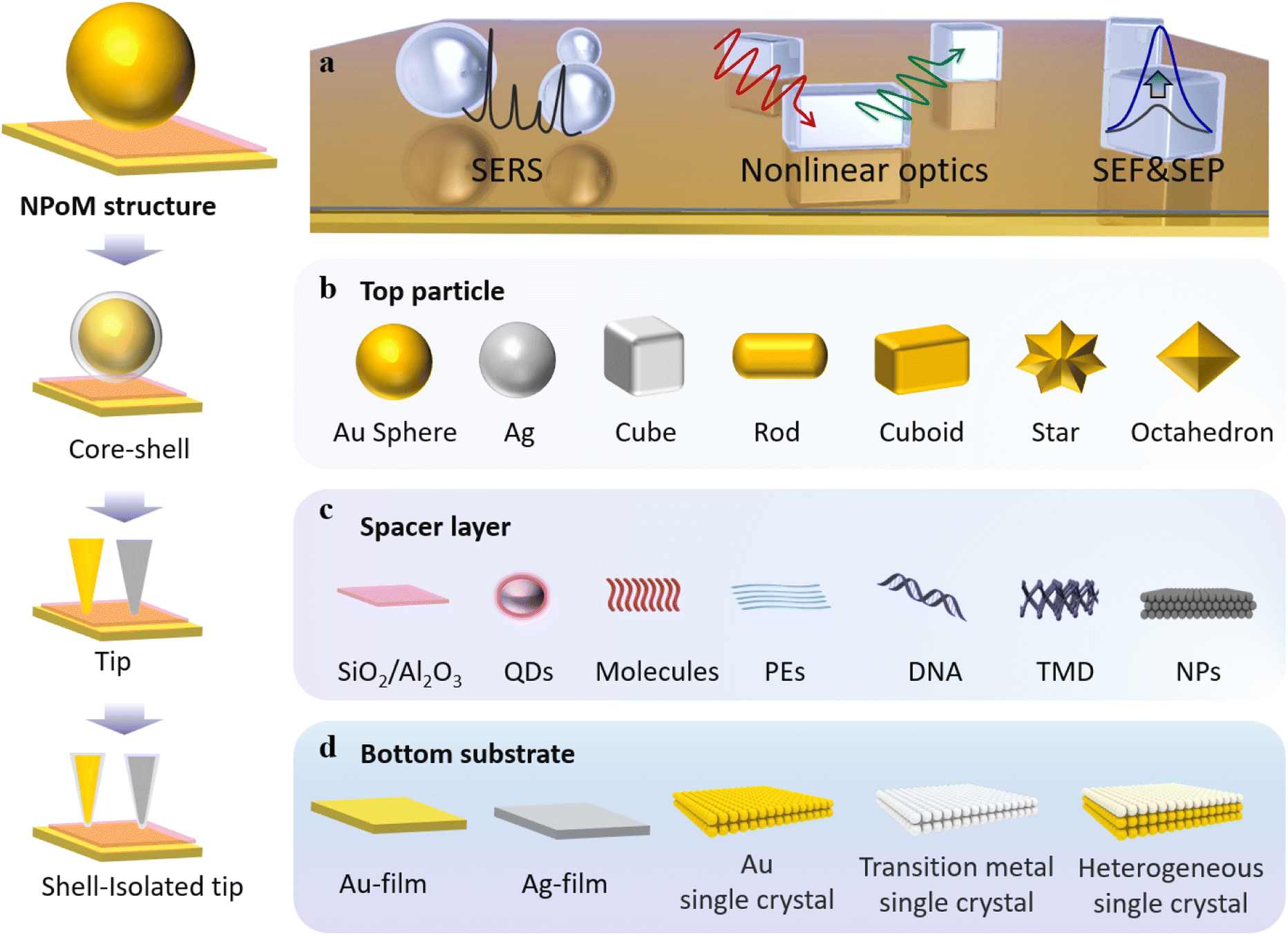 | ||
| Fig. 1 NPoM nanocavity structure. (a) Applications of the NPoM nanocavity structure. Types of top nanoparticles (b), spacer layer (c), and bottom substrates (d). | ||
From bottom to top, the NPoM nanocavity structure consists of a substrate, a spacer layer, and a nanoparticle (Fig. 1). The gap between the substrate and particle surfaces forms a plasmonic cavity, generating intense localized gap plasmon resonances. The substrate typically consists of a smooth, thin film of a noble metal, as shown in Fig. 1d. This includes Au or Ag films prepared through electron-beam evaporation,41 the ‘striping’ method,42 or synthesized using colloidal methods.43 An optimal choice for substrates is single crystals of noble metals, such as Au and Ag. Single crystals exhibit atomic-level smooth surface structures and well-defined energy states. They serve as a crucial model system that bridges theory and experimentation, allowing for precise investigations of light–matter interactions within optical cavities. Additionally, there has been further development involving the use of transition metal single crystals and heterogeneous single crystals as substrates. Heterogeneous single crystals can be prepared by depositing transition metals onto the surface of Au single crystals through underpotential deposition. The formation of nanoparticle-on-transition metal single-crystal structures enables the study of changes in surface species of transition metals, playing a crucial role in electrochemical research.11 The top nanoparticle (Fig. 1b) can take various forms and sizes, including a range of plasmonic materials. Commonly, it includes Au and Ag spheres,44 cubes,45 rods, octahedra, and more.3 The spacer layer (Fig. 1c) can be any of the following materials: SiO2, Al2O3,46 quantum dots, molecules,39 luminescent groups,47 polyelectrolytes (PEs),48,49 DNA, transition metal dichalcogenides (TMDs) or other two-dimensional materials like graphene,50,51 small-sized nanoparticles, and others. Serving as a precisely dimensioned dielectric layer, the spacer layer separates the top particles from the bottom substrate while allowing for the embedding of probes within the optical cavity. Small-sized nanoparticles, such as TiO2, can also serve as the spacer layer. For instance, by constructing an Au nanoparticle–TiO2–Pt structure, it can be used to monitor hydrogen spillover phenomena in catalysis.52
It is worth noting that the NPoM model, formed by the coupling of metal nanoparticles with a substrate, can be subdivided. Researchers have differentiated between “nanocavities” and “picocavities” based on the range of volumes or effective wavelengths. Generally, the effective wavelength range for “picocavities” is approximately 0.1 nm, while that of “nanocavities” is around 1 nm.31 Besides, “picocavities” exhibit smaller volumes than “nanocavities.” For instance, the research group led by Professor Jeremy J. Baumberg reported a plasmonic picocavity formed by the coupling of a gold film and a gold nanoparticle, with a volume less than 1 nm3.53 Furthermore, they demonstrated that such plasmonic cavities can strongly couple with individual molecules at room temperature.54 In this review, we only delve into discussions on weak coupling. For a comprehensive understanding and elucidation of the phenomenon and mechanisms of coupling phenomena, such as strong coupling or single-molecule dipole coupling interactions, reference to these excellent studies is recommended.53–56
Based on the NPoM nanocavity structure, the following model has been developed: the core–shell particle-spacer-substrate model (Fig. 1). This model enables the direct measurement of signals originating from the interface between the substrate and particles. The shell layer surrounded by particles acts as a shield against external environmental interference. Additionally, the development of the tip-spacer-substrate model and the shell-isolated tip-spacer-substrate model has also been achieved. Strictly speaking, these two models cannot be classified as NPoM nanocavity structures. However, these models share many common features with the NPoM nanocavity structure; therefore, we have also provided a detailed description of their applications. In both models, the tip can also serve as a nanoparticle. Compared to the NPoM nanocavity structure, the tip-spacer-substrate model and the shell-isolated tip-spacer-substrate model demonstrate superior flexibility in terms of their in situ operability. Within the framework of the tip-spacer-substrate model, innovative techniques such as tip-enhanced Raman spectroscopy (TERS) and tip-enhanced photoluminescence (TEPL) have been developed.55–58 The flexibility of the tip imparts unique advantages to these techniques. TERS and TEPL techniques offer sub-nm resolution capabilities and have found extensive applications in high-resolution research studies. Next, we will delve into the applications of the aforementioned NPoM nanocavity structure in the realm of enhanced spectroscopy.
3. Applications in dark-field scattering spectroscopy and plasmon-enhanced spectroscopy
The NPoM structure exhibits extreme field confinement and enhancement,59 allowing plasmonic sensors to detect the characteristics of gaps with ultra-high sensitivity. Detection relies on two aspects: (1) the far-field extinction properties inherent to the nanostructure itself; (2) the combination of the characteristic spectral information (scattering, emission, absorption, etc.) of probes (probes can be a suitable research entity within the spacer layer in Fig. 1c) with the near-field enhancement of plasmonic sensors, which allows for achieving detection limits at the single-molecule level within the gap region.60,61The NPoM structure serves as a nanocavity capable of confining light within a volume significantly smaller than the wavelength of light. Within this resonator, the optical field enhancement is directly proportional to the Q/V, where (Q) represents the cavity's quality factor, and (V) is the mode volume. To enhance the optical field, it is necessary to increase (Q) or decrease (V). LSPR is coupled into the metal nanoparticles after the excitation of photons, leading to relaxation through radiative and non-radiative processes.62,63 Radiative relaxation involves the emission of photons outward, while non-radiative relaxation manifests as the absorption of the excited light. Both of these loss mechanisms affect the quality factor of the cavity. The quality factor (Q) is given by Q = πτ/T, where τ is the lifetime of the surface plasmon and T is the oscillation period. According to theoretical studies, the lifetime τ of surface plasmons is related to the spectral linewidth (Γ) of the plasmon through the following equation:64
In this section, we will first introduce research on the extinction properties utilizing the NPoM structure. Subsequently, the use of the NPoM structure in achieving higher enhancement capabilities and spatial resolution in spectroscopic studies is emphasized. These spectroscopic studies encompass advancements and prospects in plasmon-enhanced Raman, PL (including fluorescence, phosphorescence, and upconversion), ECL, and CL.
3.1 Dark-field scattering spectroscopy
The extinction properties of the NPoM structure are influenced by various factors, including the material, size, and shape of the top nanoparticles; the material and thickness of the particle protectant; the bottom substrate material and its roughness; the dimensions of the nanocavities (the distance between metal nanoparticles and the substrate); as well as the dielectric environment.65 By measuring the dark-field scattering spectra, we can detect variations of these factors with extremely high sensitivity. The optical properties of the NPoM structure can be affected by atomic-scale variations in the facets, edges, and vertices. Consequently, even nanoparticles with the same diameter may exhibit significant differences in their dark-field scattering spectra, especially when the gap dimensions are extremely small. Therefore, constructing a well-designed nanocavity is crucial for studying the dark-field scattering spectra of nanostructures or probing the characteristic spectral information of probes.To explore highly sensitive variations in vertical dimensions (cavity size variations), Professor Xu's group developed a straightforward experimental setup based on nanowire-on-mirror (NWoM) plasmonic nanostructures (Fig. 2a).66 The setup comprises an Au nanowire (NW) coated with a layer of hexadecyltrimethylammonium bromide (CTAB) molecules on the top, an ultrasmooth Au film at the bottom, and Al2O3 layers of varying thicknesses ranging from 5.0 nm to 0.5 nm. The thickness of CTAB can be reduced to 0.5 nm through cleaning, and the roughness of the ultrasmooth Au film is ∼0.32 nm. Minimizing the thickness of the surface protectant and utilizing an ultrasmooth Au film is essential, because smaller-sized nanocavities exhibit stronger confined cavity plasmon resonances, resulting in heightened sensitivity to substrates and particles.
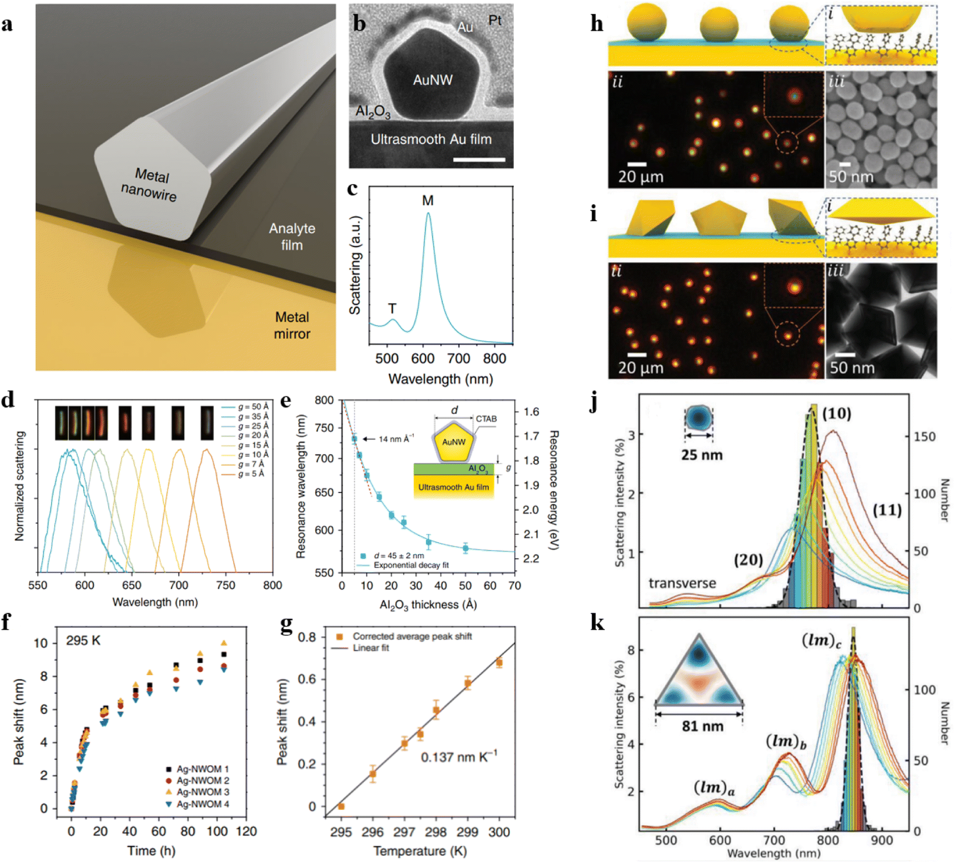 | ||
| Fig. 2 (a) Model diagram of the NWoM system. (b) TEM image of an individual NWoM system: a crystalline AuNW with a pentagonal cross-section positioned on the gold film, separated by a 1.5 nm Al2O3 spacer. Additionally, an 8 nm Al2O3 layer is applied to the NWoM's surface to enhance the nanowire's shape visibility. Scale bar, 30 nm. (c) The calculated scattering spectrum: a 45 nm-diameter AuNW on the gold film with a 2 nm vacuum separation. (d) Dark-field spectra of individual Au-NWoM systems separated by an Al2O3 film with thickness ranging from 0.5 to 5.0 nm. The insets show the corresponding dark-field images. (e) Measured resonant peak (plasmon resonance energy) of the cavity plasmon of the Au-NWoMs versus the Al2O3 thickness. (f) Spectral shift effect at 295 K as a function of measurement time from four individual Ag-NWoMs. (g) Temperature-dependent average shift of the resonance wavelength purely induced by the thermal expansion effect of the PVP layer. Panels (a)–(g) are reprinted with permission from ref. 66, under the Creative Commons Attribution 4.0 Public License. Schematics, dark-field and SEM images of (h) NPoMs and (i) NDoMs. Histograms of the dominant cavity mode wavelengths, together with average spectra from each bin of (j) D = 80 nm NPoMs with facets (typically 25 nm), and (k) Redge = 81 nm NDoMs. Panels (h)–(k) are reprinted with permission from ref. 67, under the Creative Commons Attribution 4.0 Public License. | ||
The bottom surface of the nanowire forms a metal–insulator–metal nanocavity with the thin metal film (as shown in Fig. 2b). This device exhibits a sensitive cavity-plasmon resonance. Theoretical simulations indicate that the scattering spectrum of this system presents two resonant peaks, as depicted in Fig. 2c, denoted as the T peak and the M peak. The T peak corresponds to the transverse dipole mode of the nanowire itself, while the M peak originates from the lowest frequency cavity-plasmon mode. By employing atomic layer deposition, it is possible to control the thickness of the Al2O3 spacer layer. As illustrated in Fig. 2d, with a reduction in the thickness of the Al2O3 layer, the plasmon resonance spectrum exhibits a redshift in emission. Fig. 2e provides an insight into how the resonance wavelength and energy change with Al2O3 thicknesses. The most significant alteration occurs when the cavity size is at its minimum, with a value of 14 nm Å−1.
However, the above-mentioned methods involve non-in situ alteration of the thickness of Al2O3. To enable in situ investigations, they also employed Ag NWs coated with polyvinyl pyrrolidone (PVP) as a protective agent. By conducting dark-field scattering measurements on Ag-NWoM at a constant temperature, they observed an irreversible redshift in the peak position over time (Fig. 2f). This shift could be attributed to the deformation of the PVP layer due to the weight of AgNWs or the release of water molecules.
In order to investigate how the Ag-NWoM structure responds to the environmental temperature, the researchers systematically varied the temperature range from 295 K to 300 K. During this process, the resonance peak shift encompassed both the reversible thermal expansion effect of the PVP layer and the irreversible redshift effect of the sample. By subtracting the time-dependent irreversible redshift, the net spectral shift induced by temperature-related thermal expansion was ultimately determined to be 0.137 nm K−1 (Fig. 2g).
The aforementioned study demonstrates how harnessing the plasmonic resonance characteristics of nanocavities enables high-resolution monitoring of changes in materials, environmental conditions, and optical cavity dimensions. To tackle the challenges associated with controlling particle crystal facets and to deepen our understanding of light coupling, Professor Jeremy J. Baumberg's research group developed a nano-cavity based on Au nanodecahedra.67 Utilizing an automated particle tracking system, they investigated over 20![[thin space (1/6-em)]](https://www.rsc.org/images/entities/char_2009.gif) 000 individual nano-cavities, systematically comparing the scattering spectra and SERS enhancement capabilities of NPoM nanocavities and nanodecahedron-on-mirror (NDoM) nanocavities.
000 individual nano-cavities, systematically comparing the scattering spectra and SERS enhancement capabilities of NPoM nanocavities and nanodecahedron-on-mirror (NDoM) nanocavities.
Specifically, they first coated the Au film with a monolayer of biphenyl-4-thiol molecules in advance. Subsequently, they assembled Au particles (80 nm diameter) synthesized using the sodium citrate method. Typically, nanoparticles synthesized using the sodium citrate method exhibit a wide size distribution and are not perfectly spherical, as evidenced by dark-field optical microscopy images and scanning electron microscopy (SEM) images (Fig. 2h). According to their scattering spectra, the distribution range of the dominant mode wavelength exceeds 100 nm, and there is significant variation in scattering intensity (Fig. 2j). In contrast, for NDoMs, the consistency of peak intensity and position is significantly superior to that of NPoMs (see Fig. 2i and k).
They also demonstrated the remarkable sensitivity of plasmonic nano-cavities with dimensions on the order of a few nm to crystal facets. NPs synthesized through the conventional sodium citrate method encounter challenges in efficiently managing crystal facets, resulting in considerable fluctuations in both cavity modes and field enhancements. Through the statistical analysis of over 20000 such structures, they have found that NDoM structures exhibit better SERS performance due to their precise crystal facet size and shape. These findings indicate that in small-sized optical cavities, plasmonic properties are influenced not only by well-known factors such as the particle morphology, cavity dimensions, and dielectric environment but also by crystal facets. Therefore, caution should be exercised when assuming that cavity modes and field enhancements remain consistent in constructed fixed-size cavities with particles of similar size.
3.2 Surface-enhanced Raman spectroscopy
Dark-field scattering spectroscopy provides an exceptionally sensitive tool for examining alterations in the dimensions of nano-sized gaps and variations of the dielectric environment. Additionally, when combined with molecular-specific spectroscopy and the near-field enhancement of plasmonic sensors, it not only allows for a comprehensive understanding of field distribution within optical cavities but also facilitates the detection of changes in molecular species within these gap regions.68 This has substantial relevance for investigating intermediate products and mechanisms in energy and catalysis-related reactions.There are many excellent reviews available on the origin and principles of SERS.69–71 The intensity of SERS enables a direct examination of field distribution within the optical cavity with remarkable spatial resolution capabilities. In this section, we will primarily focus on recent advancements achieved through the utilization of SERS. We'll begin by taking the advantage of molecules and TMDs as “plasmonic rulers” to elucidate field distributions within the optical cavity at the Ångstrom scale. Additionally, we will introduce the application of in situ Raman spectroscopy in studying the structure and dissociation of water molecules at the interface between particles and single crystals. The results will demonstrate that SERS not only can serve as a fingerprint spectroscopy technique for investigating changes in molecular species but also play a valuable role in in situ analysis of alterations in the molecular structure. These findings open up new avenues for the applications of Raman spectroscopy.
The existence of non-uniformity in the localized electric field within a nanocavity is widely acknowledged. However, investigating the actual distribution of this field inside the nanocavity presents considerable challenges, especially when striving for ultra-high resolution at the Ångstrom level. This challenge arises from the need to achieve the required level of sensitivity for detecting extremely small changes at the Ångstrom scale. This necessitates the development of exceptionally advanced experimental setups. As a result, the development of a sophisticated experimental apparatus for directly measuring the field distribution within a nanocavity is considered a paramount task.
Based on this, our group devised a well-considered optical cavity structure and successfully overcame this challenge.72 By utilizing SERS to measure the electric field distribution within the nanocavity, we ultimately achieved a spatial resolution of 2.2 Å. This nanocavity comprises an Au(111) surface and an Au nanoparticle coated with a SiO2 shell. The self-assembled viologen molecular monolayer with a specific probe moiety was positioned within the nanocavity (Fig. 3a). The position of the probe moiety was continuously shifted along the viologen molecule, differing by an ethyl unit (Fig. 3b). As depicted in Fig. 3c, we compared the Raman spectra of molecules at different probe positions and statistically analyzed their characteristic peak intensities (the trend analysis of Raman intensity or peak area variations at different positions within the optical cavity can be conducted by normalizing the Raman spectral intensity of characteristic peaks or the Raman peak area (divided by the numerical value of the maximum), Fig. 3e). Thus, we were able to determine the electric field distribution within the nanocavity through the relationship between the spatial position of the probe and Raman intensity. With the assistance of first-principles calculations, we validated the non-uniformity of the electric field within the optical cavity (Fig. 3d and f). This study introduces a new method to measure the electric field distribution within an optical cavity quantitatively. Using plasmonic-enhanced Raman spectroscopy, achieves exceptionally high resolution, helping us better understand optical cavities and plasmonic systems. However, the random orientation of molecules and vibration directions during adsorption may lead to varying SERS intensities on the same substrate. TMD crystals offer a solution due to their well-defined crystal orientations and sub-nanometre thickness.73,74 The research team, led by Tian and Yang, employed four layers of MoS2 and a monolayer of WS2 transferred onto a nanoparticle-on-mirror structure. They used the monolayer WS2 as a probe and placed it at different interlayer spacings. By measuring the Raman signal of WS2 at various positions within the optical cavity, they could quantitatively determine the longitudinal plasmonic field distribution.74
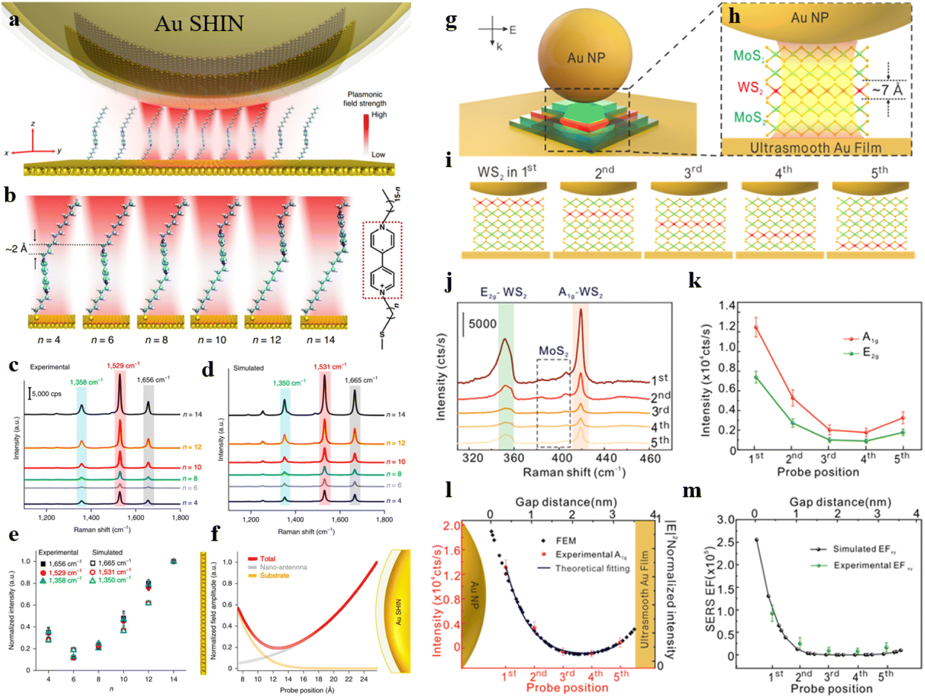 | ||
| Fig. 3 (a) Experimental setup schematic. (b) The simulated conformations of different viologen molecules. Experimental SERS spectra (c) and simulated Raman spectra (d) of different viologen molecules. (e) Normalized experimental and simulated Raman intensities. (f) Normalized electric field amplitude for viologen molecules in the cavity. Panels (a)–(f) are reprinted with permission from ref. 72, Copyright from 2020, Nature Publishing Group. (g) Schematic representation of a nanocavity. (h) An enlarged view of the designated area in (g). (i) Diagrams of WS2 at different positions. (j) SERS spectra obtained from WS2 at different positions. (k) SERS intensity of A1g and E2g as a function of the location of WS2 within various layers. (l) The variation of experimental and theoretical data with the position of the probes. (m) Experimental and theoretical SERS enhancement factor (EFxy) of E2g in various positions. Panels (g)–(m) are reprinted with permission from ref. 74, Copyright from 2022, American Chemical Society. | ||
As shown in Fig. 3g, TMDs are positioned between the Au film substrate and a single Au nanoparticle. Fig. 3h illustrates the placement of WS2 on the third layer, with each layer of the two-dimensional atomic crystal approximately 0.7 nm. WS2 is positioned as the first layer in proximity to the Au nanoparticle and as the fifth layer near the Au film (Fig. 3i). The authors measured the SERS spectra of WS2 at different positions within the optical cavity (Fig. 3j) and statistically analyzed the intensities E2g and A1g peaks of WS2 (Fig. 3k). Combining with theoretical simulations, it was demonstrated that when WS2 transitions from the first layer to the fifth layer, the SERS intensity of the A1g peak exhibits a trend of first decreasing and then increasing (Fig. 3l and m).
The aforementioned results have laid a foundation for a deeper understanding of the distribution of the field within the optical cavity. However, due to the differences among particles (even when they have similar size and morphology), measurements can still introduce a certain level of inaccuracies. As discussed in Section 3.1, within fixed-size NPoM cavities, even though the particle sizes are similar, there will still be certain differences in the corresponding cavity modes and field enhancements. Consequently, challenges arising from variations between particles or positions are difficult to eliminate, potentially complicating the study of changes within a system. Therefore, the realization of in situ measurement is the main trend of the future development of spectroscopy.
Recently, there has been a growing interest in using in situ SERS to study interface electrocatalytic reactions, providing insights into reaction mechanisms. For instance, as the most crucial participants in electrocatalytic reactions, the behaviours of water molecules have a direct impact on the entire electrocatalytic process at the electrode/electrolyte interface. However, due to the fickle structures of water molecules, the extremely low content of interfacial water, and the complex interfacial environment, the study of water molecules at the electrode/electrolyte interface remains a significant challenge. This limitation hinders the comprehensive molecular-level understanding of the structure–performance relationship between interfacial water molecules and electrocatalytic mechanisms. Therefore, establishing and advancing high-sensitivity in situ spectroscopic characterization techniques to thoroughly investigate the behaviour of water molecules at the electrode/electrolyte interface and uncover their pivotal roles in electrocatalytic reaction processes are crucial scientific endeavours in the field of fundamental interfacial electrocatalysis research.
The shell-isolated nanoparticle-enhanced Raman spectroscopy (SHINERS) technique, pioneered by our team, has successfully overcome the longstanding limitations of SERS technology, allowing for the enhancement of Raman signals on single crystal surfaces.10 However, in the widely applied realm of electrocatalysis, the coupling-enhancement effect between transition metal single crystal electrodes (non-plasmonic materials) and Au@SiO2 is notably weak. To address this bottleneck, our group has recently developed a unique structure referred to as Au@SiO2-on-heterogeneous metal single crystal nanocavities (Fig. 4a).11 The top Au@SiO2 nanoparticle not only eliminates the interference from molecules in the bulk phase but also enables the acquisition of Raman signals from water molecules at the particle–single crystal interface. Heterogeneous single crystals, depicted as white atoms in Fig. 4a, were fabricated by underpotentially depositing transition metals onto the surface of Au single crystals (depicted as yellow atoms). By leveraging the strong coupling between the Au single crystal and the Au@SiO2, we enhanced the signals on the surface of the transition metal single crystal electrode. Three-dimensional time-domain finite-difference simulation results demonstrate that this nanocavity structure can achieve a maximum enhancement factor of up to 108 on the surface of the transition metal single crystal. As illustrated in Fig. 4b, the strong signal enhancement arises from the electromagnetic field at the junction between Au@SiO2 and the substrate, indicating that this model allows the observation of Raman signals from water molecules near the ‘hotspots.’ As a result, the Au@SiO2-on-heterogeneous metal single crystal electrode structure significantly enhances the sensitivity of Raman spectroscopy detection, offering a new avenue for in situ spectroscopic research on water molecules at the electrode/electrolyte interface.
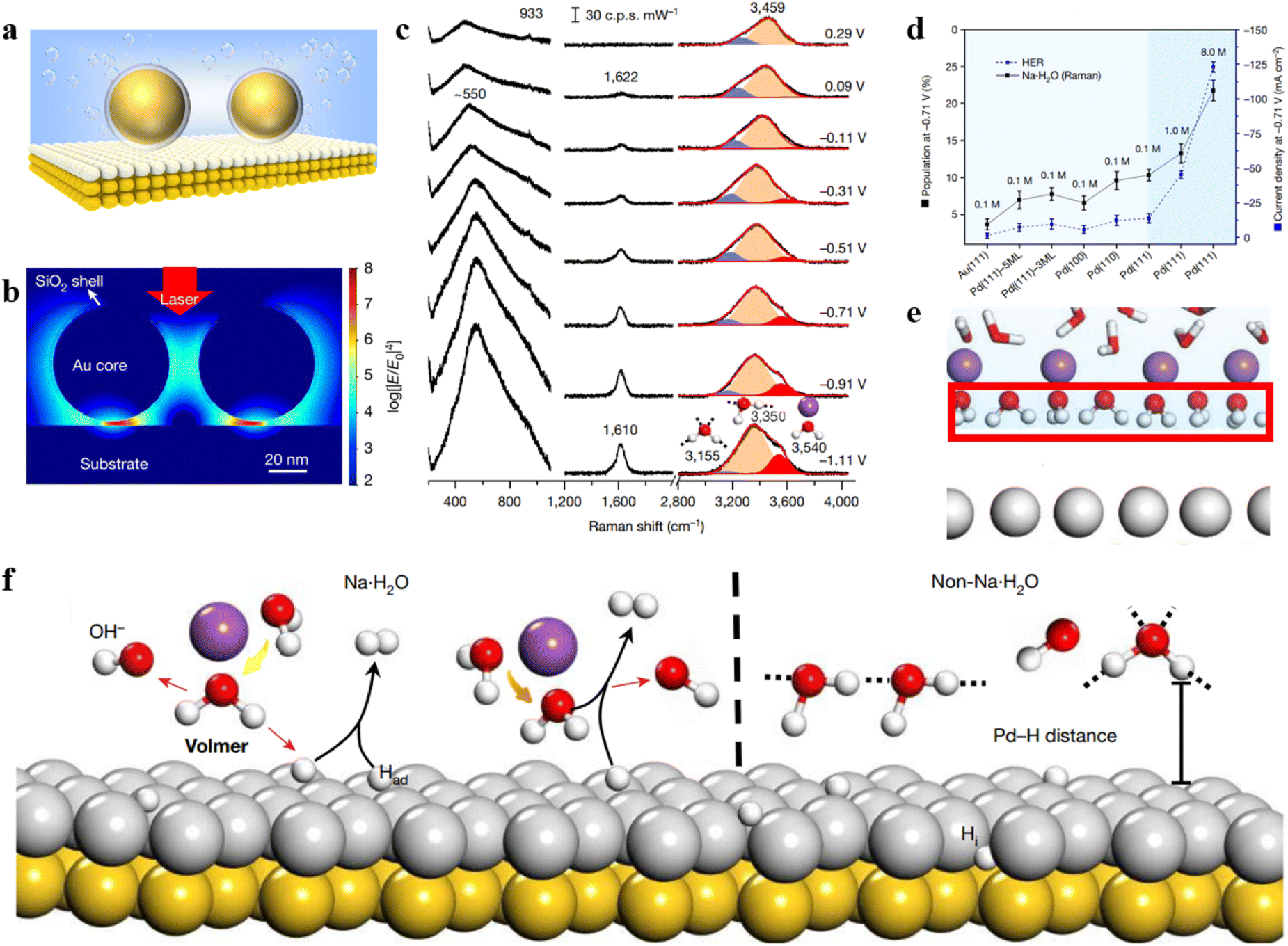 | ||
| Fig. 4 (a) Structure of Au@SiO2-on-heterogeneous metal single crystal nanocavities. (b) Simulated Raman enhancement effect. (c) In situ Raman spectroscopy results of water molecules at the Pd(111) interface under alkaline conditions. (d) Variation in the concentration of hydrated water molecules on different electrode surfaces and HER current density at −0.71 V under different electrolyte concentrations. (e) Schematic representation of ordered interfacial water molecules. (f) Dissociation process of Na·H2O molecules and HB·H2O molecules on the electrode surface. Panels (b)–(f) are reprinted with permission from ref. 11, Copyright from 2021, Springer Nature Limited. | ||
Based on this method, in situ monitoring of the configuration and dynamic changes of water molecules at the Pd single crystal electrode/electrolyte interface was conducted using electrochemical in situ Raman spectroscopy, as shown in Fig. 4c. The study revealed that the interfacial water contains hydrogen-bonded water (HB·H2O) and Na+ ion hydrated water (Na·H2O). The population of Na·H2O exhibits a strong correlation with hydrogen evolution performance (Fig. 4d). Spectral evidence and ab initio molecular dynamics simulations unveiled that under the synergistic effect of cations and electrode potential the interfacial water molecules form a more ordered structure at negative potential (Fig. 4e). The Na·H2O is closer to the electrode surface than HB·H2O (Fig. 4f), thereby promoting the charge transfer efficiency between the water molecule and electrode, which caused a great improvement in the rate of the hydrogen evolution reaction. By increasing the concentration and valence state of cations, the population of ordered interfacial water molecules is further improved, consequently promoting the rate of the hydrogen evolution reaction.
The study also discovered that both the crystal facet and electronic structure of the single crystal electrode influence the content of cation-hydrated water molecules and the rate of the hydrogen evolution reaction. This work confirms the universality of the strategy in promoting the hydrogen evolution reaction rate through cation regulation of interfacial water. Commencing from a single crystal model system, this work deeply comprehends the regulatory mechanism of the interfacial water molecule structure on electrocatalytic reaction processes. It addresses a long-standing issue in the field of electrochemistry and provides a new strategy for enhancing the rate of electrocatalytic reactions.
3.3 Surface-enhanced fluorescence spectroscopy
At present, SEF, has evolved into a highly sensitive spectroscopic technique with powerful characterization capabilities.5,75 For an introduction, development history, and mechanistic description of SEF, please refer to previously published excellent literature.76–81 Unlike SERS, SEF exhibits fluorescence quenching when fluorescent molecules are located on or very close to metal structures (<5 nm).42 This limitation not only restricts the applications of SEF but also imposes stringent constraints on achieving high spatial resolution. Research indicates that as the distance between fluorescent molecules and metals gradually increases on the nanometre scale, there is a transition from fluorescence quenching to fluorescence enhancement.82 Consequently, the development of shell-isolated nanoparticle-enhanced fluorescence (SHINEF) is employed to investigate the interaction between fluorescent molecules and metals at the nanoscale.77,83 The current challenges in SEF include the development of spectroscopic methods with ultra-high enhancement to explore the “limits” of enhancement and the construction of appropriate experimental setups to achieve high spatial resolution.The NPoM structure has found extensive applications and achieved significant breakthroughs in the field of SEF. For instance, Professors D. R. Smith and Maiken H. Mikkelsen have made numerous pioneering contributions in this area.29,39,45,47,48,65,75,84 They systematically studied the spontaneous emission rate/lifetime, quantum yield, and changes in the emission direction of fluorescent molecules by embedding probes between particles and substrates. These efforts laid the foundation for precise research into the interactions between nanostructures and fluorescent molecules. It is widely accepted that, through the judicious design of NPoM structures, the spontaneous emission rate of fluorescent molecules (including radiative and non-radiative transition rates) can be tremendously enhanced. Current research indicates that the fluorescence lifetime can be shortened by over 1000 times while maintaining a high quantum efficiency (>0.5) and directional emission (high collection efficiency).47
In the realm of enhanced PL, NPoM structures also demonstrate its universality. When fluorescent molecules are replaced with QDs,85 TMDs, or other luminescent materials, their luminescent properties can also be enhanced. Notably, compared to traditional fluorescent molecules, graphene QDs offer advantages such as high photostability, low cytotoxicity, excellent biocompatibility, and good water solubility. Incorporating graphene QDs into NPoM structures provides an effective approach for high-speed displays and high-speed visible-band quantum communication.86 TMDs possess outstanding optoelectronic and fluorescence properties. Integrating TMDs into NPoM structures holds promise for applications in optoelectronic devices and sensors.50,87
In recent years, tip-enhanced fluorescence spectroscopy (TEFS) and shell-isolated tip-enhanced fluorescence spectroscopy techniques have undergone rapid development. Both of these techniques involve the creation of a nanoscale optical cavity between the tip and the substrate, which is similar to the NPoM structure in nature. However, these two techniques offer significant advantages in achieving high spatial resolution, enabling ultra-high-resolution surface analysis. For example, the research group led by Hou, Dong, and Zhang used TEFS to image a single zinc phthalocyanine (ZnPc) molecule.88 By demonstrating the results of PL coupling between single ZnPc molecules and nanocavity plasmons, they achieved a spatial resolution of approximately 8 Å. Furthermore, they were able to locally map the molecular exciton energy and linewidth at a sub-molecular resolution. Fig. 5a illustrates a model of the experimental setup. To prevent direct contact between ZnPc molecules and the Ag(100) substrate, the authors applied a three-layer thick layer of sodium chloride (NaCl) as a dielectric layer on top of the Ag single crystal substrate.
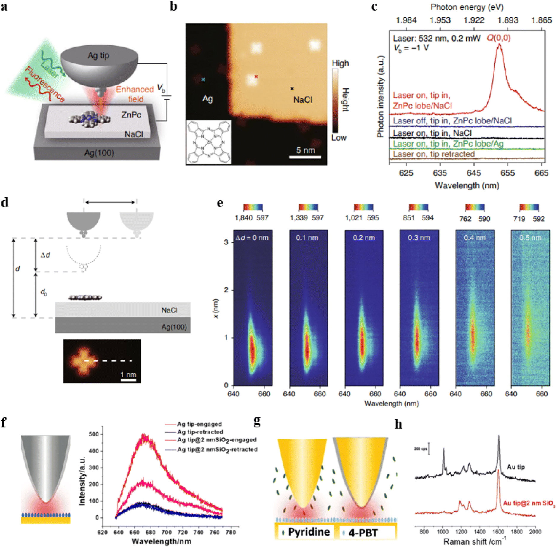 | ||
| Fig. 5 (a) Schematic of the experimental set-up. (b) STM image from a single ZnPc molecule on three-monolayer-thick NaCl/Ag(100). (c) TEPL spectra acquired at different positions. (d) Schematic of the junction geometrical parameters. (e) Spectral evolution of TEPL for the line trace shown in (d). Panels (a)–(e) are reprinted with permission from ref. 88, Copyright from 2022, Springer Nature Limited. (f) Tip-enhanced fluorescence and shell-isolated tip-enhanced fluorescence. (g) and (h) Tip-enhanced Raman and shell-isolated tip-enhanced Raman. Panels (f)–(h) are reprinted with permission from ref. 89, Copyright from 2018, Wiley-VCH Verlag GmbH & Co. KGaA, Weinheim. | ||
The silver-tip structure not only enhances photon emission rates but also enables high-resolution scanning tunnelling microscope (STM) imaging (Fig. 5b). When the tip is positioned on an isolated ZnPc molecule, the molecular emission behaviour was tested with the laser turned on (red curve) or off (blue curve). As shown in Fig. 5c, there is no noticeable specific emission when the laser is off. When the laser is on, there is a prominent emission peak around 653 nm, which is attributed to the Q(0, 0) transition of the ZnPc molecule. When the tip is positioned above the NaCl surface, there is also no emission behavior, confirming that the emission originates from the ZnPc molecules (black curve). NaCl is crucial because when ZnPc molecules are directly deposited on the bare Ag surface, the fluorescence is completely quenched (green curve). Furthermore, when the tip is fully retracted, there is also no characteristic emission (brown curve), indicating that it is necessary to construct an optical cavity through the coupling of the tip and the substrate to achieve strong fluorescence enhancement. By studying the TEPL spectra at different gap distances (Fig. 5d), it was observed that as the distance increases, the fluorescence emission gradually weakens (Fig. 5e).
The shell-isolated tip-enhanced fluorescence spectroscopy technique allows for the direct acquisition of signals from fluorescent molecules assembled on a typical substrate. Fig. 5f displays tip-enhanced fluorescence spectra obtained using an Ag tip coated with a 2 nm silica shell and bare Ag tip.89 Cyanine 5 (Cy5) molecules were assembled on the surface of an Au substrate. Due to non-radiative energy transfer between the Cy5 and the Au substrate, the fluorescence intensity of Cy5 is relatively low when the tip is retracted (black curve). Compared to the bare tip, the Ag tip coated with SiO2 can reduce non-radiative energy transfer between Cy5 and the tip, thereby obtaining a stronger fluorescence signal.
On the other hand, shell-isolated tip-enhanced Raman spectroscopy techniques combine the advantages of TERS and SHINERS techniques, allowing measurements in a solution environment. Typically, it is challenging to directly obtain signals from molecules at the substrate surface due to interference from substances or impurities in the solution. As illustrated in Fig. 5g, our research group conducted TERS measurements using both a bare Au tip and a 2 nm SiO2 shell-isolated Au tip in a solution containing pyridine, with (4′-(pyridin-4-yl)biphenyl-4-yl)methanethiol (4-PBT) molecules assembled on the Au(111) substrate. The TERS spectra obtained with the bare Au tip exhibit Raman signals from both 4-PBT and pyridine (Fig. 5h, black curve). However, when using a 2 nm SiO2 shell-isolated Au tip, only the Raman signal from 4-PBT is observed (Fig. 5h, red curve). This is because pyridine in the solution can adsorb onto the bare Au tip but not onto the SiO2 shell (pyridine does not interact with SiO2). Hence, in the presence of the SiO2 layer, the Raman signals of pyridine molecules are no longer observable. These results indicate that the ultra-thin SiO2 shell can effectively eliminate interference from substances in the solution phase, thereby aiding in the acquisition of Raman spectral signals from the substrate.
3.4 Surface-enhanced phosphorescence and upconversion luminescence
Both SERS and SEF have made significant progress, enabling enhancements of over 4 orders of magnitude. Surface-enhanced phosphorescence (SEP)90,91 and enhanced upconversion luminescence92 essentially show no difference with enhanced fluorescence. In theory, SEP is feasible by coupling phosphorescence groups with plasmon resonances.91 However, typically modest enhancements (∼10) are achieved in experiments that rely on restrictive conditions such as low temperatures and oxygen-depleted environments, which hinder the realization of SEP and impede its progress.In the early stages, Professor Geddes' group systematically investigated the factors influencing SEP under low-temperature and anaerobic conditions, establishing a strong foundation for SEP research.16,93 Future practical applications of SEP are anticipated to involve the utilization of enhanced singlet oxygen (1O2) generation for bacterial deactivation.94 For example, Professor Belinda Heyne's team immobilized the photosensitive molecule rose bengal (RB) onto Ag NCs @SiO2 surfaces with various shell thicknesses.95,96 Then, they studied the effect of varying shell thicknesses of Ag@SiO2 NCs on the generation of 1O2. The results demonstrate that the most significant enhancement in 1O2 production occurred with a shell thickness of approximately 10 nm, leading to a 12-fold increase in signal. The research team introduced Ag NCs@SiO2-RB structures into S. aureus and E. coli bacteria, analysed the bacteria's survival curves, and found that the Ag NCs@SiO2-RB structures displayed effective antibacterial properties.
However, the phosphorescence process is usually in an inherently “dark state” and effectively activating the phosphorescence process has remained a long-standing challenge. Based on this, our team recently designed an NPoM cavity, as illustrated in Fig. 6a.97 We deposited RB molecules on the top of polyelectrolytes (PEs), and PEs were carefully embedded between the Au film and Ag nanocubes (NCs). RB exhibits both fluorescence and phosphorescence emissions under low-temperature anaerobic conditions (Fig. 6b, orange curve). However, RB only emits fluorescence at room temperature (Fig. 6b, black curve). This behaviour is attributed to the influence of optical selection rules and the quenching effect from oxygen. We found that two conditions need to be met to achieve room-temperature phosphorescence emission. First, the nanocavity must possess a high spontaneous emission rate enhancement, which requires an overlap between the cavity mode and the triplet state. Second, it should have a high quantum yield, which necessitates an appropriately sized cavity. Through the combination of experimental validation and theoretical modelling, we have successfully activated the ultrafast emission of phosphorescence, achieving a remarkable enhancement in spontaneous emission rates, surpassing a factor of 1000 (Fig. 6c). This breakthrough has enabled us to overcome the challenges posed by rapid non-radiative transitions, allowing plasmonic structures to actively manipulate the radiative behaviour of phosphorescence molecules.
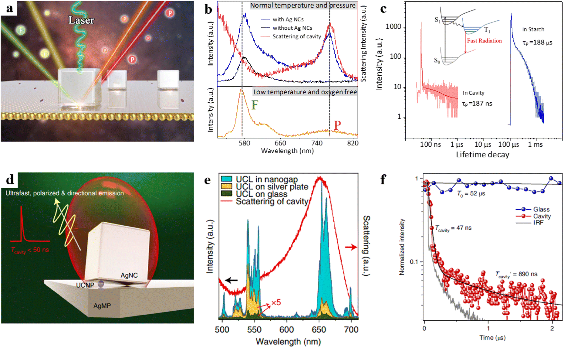 | ||
| Fig. 6 (a) Schematic diagram of the model. (b) The bottom panel is the emission spectrum of the RB at −190 °C under hypoxic conditions, the top panel is the emission spectra of the Au film surface with RB probe molecules at room temperature and the corresponding dark-field scattering spectrum. (c) Transient dynamics of RB in optical cavities and in starch. Panels (a)–(c) are reprinted with permission from ref. 97, Copyright from 2023, American Chemical Society. (d) Schematic of the tilted-nanocavity-coupled UCNP. (e) Upconversion luminescence spectra and the dark-field scattering spectrum. (f) Normalized transient dynamics of UCNPs in the tilted cavity and on the glass slide. Panels (d)–(f) are reprinted with permission from ref. 43, Copyright from 2022, Springer Nature Limited. | ||
Furthermore, rare-earth-doped upconversion nanoparticles (UCNPs) have attracted significant attention due to their advantages of stable, coherent, narrowband, and multicolour emission. Due to the 4f–4f forbidden transitions of rare-earth ions, UCNPs exhibit long emission decay times ranging from microseconds to milliseconds.98 However, the long emission decay times limit their applications in time-dependent nanophotonic devices. To address this, the Zheng research group created a tilted plasmonic nanocavity by embedding UCNPs into the cavity (Fig. 6d).43 The authors found that the luminescence intensity of the UCNP in the cavity was intensively enhanced over 60000-fold (Fig. 6e). Additionally, the emission decay rate of UCNPs could be shortened, with lifetimes below 50 ns (Fig. 6f), while maintaining a high quantum efficiency enhancement.
4. Conclusions and prospects
Metal structures at the nanoscale exhibit distinctive optical, electrical, magnetic, and thermal properties that set them apart from macroscopic metals.99,100 Their special optical characteristics bestow upon them unique potential applications, making them important subjects of research in the field of nanoscience. The spectral signals of molecules located on or near the surface of nanoparticles are significantly enhanced, thereby greatly improving the sensitivity of spectroscopic analysis.101–103 One of the most attractive metal nanostructures is the NPoM, which generates strongly confined gap plasmons between the two opposing metal surfaces. The optical properties of the NPoM are closely linked to various factors. Designing a reasonable NPoM structure helps us to understand the interaction between light and matter. This perspective provides an overview of the application of NPoM structures in surface-enhanced spectroscopy (SES) techniques, mainly including SERS, SEF, and SEP.Here, we also summarize the current state of SES and offer insights into its future developments. While SES has achieved many successes to date, there are still demands and challenges in future research. Addressing these demands and challenges will expand the scope of SES technology across various domains and enhance its analytical capabilities:
(1) In the realm of fundamental scientific research, there is an expectation to improve resolution in terms of energy, space, and time.
(2) In practical applications, there are also higher demands for the universality of surface-enhanced substrates and their forms, as well as the conditions for detection.
(3) In broader industrial and daily life applications, not only reliability and reproducibility of results are sought after, but also the convenience of monitoring and cost-effectiveness.
In addition, with the continuous advancement of science and technology, the demand for higher detection sensitivity is also growing. It is reasonable to predict that in the future, SES technology will achieve higher temporal and spatial resolution:
4.1 Time resolution
One of the future trends includes the development of surface-enhanced ultrafast time-resolved spectroscopy. This requires us to use SES technology to achieve higher temporal resolution, especially on extremely short timescales. To realize this objective, ultrafast pulse techniques like femtosecond lasers are essential for capturing the rapid dynamic processes of molecules and materials.104 For instance, by utilizing surface-enhanced substrates with femtosecond transient absorption spectroscopy, we can obtain insights into the transitions between excited states of substances, encompassing physical and chemical processes such as energy and electron transfer; through the rational design of nanomaterials and the integration of femtosecond stimulated Raman spectroscopy, we can in situ monitor interfacial dynamic processes, unveiling reaction mechanisms and structure–activity relationships at the molecular level. These studies include in-depth exploration of phenomena such as molecular vibrations and electronic transitions. These methodologies are of paramount importance for comprehending chemical reactions, biological processes, and material behaviours.4.2 Spatial resolution
Achieving higher spatial resolution, including at the nanometre, Ångström, and even sub-Ångström levels, as well as at the level of single particle and single molecule, is a crucial objective. To realize this goal, we need to employ nanoprobes, high-resolution microscopy, and nanofabrication techniques to observe and manipulate nanostructures. Dark-field scattering spectroscopy is an expression of the inherent properties of metal nanostructures. This technique enables us to observe nanostructures with high resolution, providing a deeper understanding of the characteristics of metal materials and how these attributes are interconnected with their optical behaviour. Combining SES techniques (such as TERS) with dark-field scattering spectroscopy contributes to our ability to observe the dynamic behaviours of molecules and materials in practical sensing and bioanalytical processes.In conclusion, the future development of SES techniques will prioritize achieving higher time and spatial resolution while meeting the demands for increased sensitivity. By harnessing new technologies from the fields of physics, nanotechnology, and information computing, SES techniques will expand their applications in various fields such as materials science, life science, environmental science, and nanotechnology. These advancements will provide us with more profound and precise analytical and comprehension tools.
Author contributions
W. P. outlined and wrote the manuscript, with contributions from all authors in the discussion and revision of the work. Y. J. Z. and J. F. L. conceptualized and supervised the completion of the manuscript.Conflicts of interest
There are no conflicts to declare.Acknowledgements
This research was supported by the National Key Research and Development Program of China (2019YFA0705400) and the National Natural Science Foundation of China (21925404, 22104124, T2293692, and 22021001).References
- J. E. Park, J. Kim and J. M. Nam, Chem. Sci., 2017, 8, 4696–4704 RSC.
- N. Jiang, X. Zhuo and J. Wang, Chem. Rev., 2018, 118, 3054–3099 CrossRef CAS PubMed.
- M. Rycenga, C. M. Cobley, J. Zeng, W. Li, C. H. Moran, Q. Zhang, D. Qin and Y. Xia, Chem. Rev., 2011, 111, 3669–3712 CrossRef CAS.
- T. You, Y. Gao, H. Chen and P. Yin, Plasmonics, 2021, 16, 1231–1239 CrossRef CAS.
- M. Pelton, Nat. Photonics, 2015, 9, 427–435 CrossRef CAS.
- X. Yang, M. Yang, B. Pang, M. Vara and Y. Xia, Chem. Rev., 2015, 115, 10410–10488 CrossRef CAS.
- J. Krajczewski and A. Kudelski, Front. Chem., 2019, 7, 410 CrossRef CAS PubMed.
- F.-L. Zhang, J. Yi, W. Lin, E.-M. You, J.-S. Lin, H. Jin, W. Cai, Z.-Q. Tian and J.-F. Li, Nano Today, 2022, 44, 101464 CrossRef CAS.
- M. Ringler, A. Schwemer, M. Wunderlich, A. Nichtl, K. Kurzinger, T. A. Klar and J. Feldmann, Phys. Rev. Lett., 2008, 100, 203002 CrossRef CAS.
- J. F. Li, Y. F. Huang, Y. Ding, Z. L. Yang, S. B. Li, X. S. Zhou, F. R. Fan, W. Zhang, Z. Y. Zhou, D. Y. Wu, B. Ren, Z. L. Wang and Z. Q. Tian, Nature, 2010, 464, 392–395 CrossRef CAS PubMed.
- Y.-H. Wang, S. Zheng, W.-M. Yang, R.-Y. Zhou, Q.-F. He, P. Radjenovic, J.-C. Dong, S. Li, J. Zheng, Z.-L. Yang, G. Attard, F. Pan, Z.-Q. Tian and J.-F. Li, Nature, 2021, 600, 81–85 CrossRef CAS PubMed.
- M. Su, C. Wang, T. Wang, Y. Jiang, Y. Xu and H. Liu, Anal. Chem., 2020, 92, 6941–6948 CrossRef CAS.
- J. R. Lakowicz, Anal. Biochem., 2005, 337, 171–194 CrossRef CAS PubMed.
- J. R. Lakowicz, K. Ray, M. Chowdhury, H. Szmacinski, Y. Fu, J. Zhang and K. Nowaczyk, Analyst, 2008, 133, 1308–1346 RSC.
- Y. Wu, J. Xu, E. T. Poh, L. Liang, H. Liu, J. K. W. Yang, C. W. Qiu, R. A. L. Vallee and X. Liu, Nat. Nanotechnol., 2019, 14, 1110–1115 CrossRef CAS.
- H. Mishra, B. L. Mali, J. Karolin, A. I. Dragan and C. D. Geddes, Phys. Chem. Chem. Phys., 2013, 15, 19538–19544 RSC.
- Y. Wei, Y. Zhang, J. Pan, T. Chen, X. Xing, W. Zhang and Z. Lu, Angew. Chem., Int. Ed., 2023, 135, e202214103 CrossRef.
- K. Aslan and C. D. Geddes, Chem. Soc. Rev., 2009, 38, 2556–2564 RSC.
- F. Neubrech, C. Huck, K. Weber, A. Pucci and H. Giessen, Chem. Rev., 2017, 117, 5110–5145 CrossRef CAS.
- E. C. Dreaden, A. M. Alkilany, X. Huang, C. J. Murphy and M. A. El-Sayed, Chem. Soc. Rev., 2012, 41, 2740–2779 RSC.
- J. M. Kim, C. Lee, Y. Lee, J. Lee, S. J. Park, S. Park and J. M. Nam, Adv. Mater., 2021, 33, 2006966 CrossRef CAS PubMed.
- H.-J. Wang, J.-S. Lin, H. Zhang, Y.-J. Zhang and J.-F. Li, Acc. Mater. Res., 2022, 3, 187–198 CrossRef CAS.
- J. E. Park, Y. Lee and J. M. Nam, Nano Lett., 2018, 18, 6475–6482 CrossRef CAS.
- G. A. Vinnacombe-Willson, Y. Conti, A. Stefancu, P. S. Weiss, E. Cortes and L. Scarabelli, Chem. Rev., 2023, 123, 8488–8529 CrossRef CAS PubMed.
- S. Lee, K. Sim, S. Y. Moon, J. Choi, Y. Jeon, J. M. Nam and S. J. Park, Adv. Mater., 2021, 33, e2007668 CrossRef.
- J. S. Lin, X. D. Tian, G. Li, F. L. Zhang, Y. Wang and J. F. Li, Chem. Soc. Rev., 2022, 51, 9445–9468 RSC.
- A. Kumar, S. Kim and J. M. Nam, J. Am. Chem. Soc., 2016, 138, 14509–14525 CrossRef CAS PubMed.
- D. Liu, L. Fang, F. Zhou, H. Li, T. Zhang, C. Li, W. Cai, Z. Deng, L. Li and Y. Li, Adv. Funct. Mater., 2018, 28, 1707392 CrossRef.
- E. Oksenberg, I. Shlesinger, A. Xomalis, A. Baldi, J. J. Baumberg, A. F. Koenderink and E. C. Garnett, Nat. Nanotechnol., 2021, 16, 1378–1385 CrossRef CAS.
- S. Lee, J. Korean Phys. Soc., 2022, 81, 502–509 CrossRef.
- J. J. Baumberg, J. Aizpurua, M. H. Mikkelsen and D. R. Smith, Nat. Mater., 2019, 18, 668–678 CrossRef CAS.
- C. Readman, B. de Nijs, I. Szabo, A. Demetriadou, R. Greenhalgh, C. Durkan, E. Rosta, O. A. Scherman and J. J. Baumberg, Nano Lett., 2019, 19, 2051–2058 CrossRef CAS PubMed.
- Z. Zhang, W. Shen, J. Xue, Y. Liu, Y. Liu, P. Yan, J. Liu and J. Tang, Nanoscale Res. Lett., 2018, 13, 54 CrossRef PubMed.
- L. Wang, M. Hasanzadeh Kafshgari and M. Meunier, Adv. Funct. Mater., 2020, 30, 2005400 CrossRef CAS.
- J. Zheng, X. Cheng, H. Zhang, X. Bai, R. Ai, L. Shao and J. Wang, Chem. Rev., 2021, 121, 13342–13453 CrossRef CAS PubMed.
- K. Yang, X. Yao, B. Liu and B. Ren, Adv. Mater., 2021, 33, e2007988 CrossRef.
- H. D. Yu, M. D. Regulacio, E. Ye and M. Y. Han, Chem. Soc. Rev., 2013, 42, 6006–6018 RSC.
- Y.-M. Bahk, D.-S. Kim and H.-R. Park, Adv. Opt. Mater., 2019, 7, 1800426 CrossRef.
- C. Ciraci, R. T. Hill, J. J. Mock, Y. Urzhumov, A. I. Fernandez-Dominguez, S. A. Maier, J. B. Pendry, A. Chilkoti and D. R. Smith, Science, 2012, 337, 1072–1074 CrossRef CAS PubMed.
- A. Moreau, C. Ciraci, J. J. Mock, R. T. Hill, Q. Wang, B. J. Wiley, A. Chilkoti and D. R. Smith, Nature, 2012, 492, 86–89 CrossRef CAS PubMed.
- J. B. Lassiter, F. McGuire, J. J. Mock, C. Ciraci, R. T. Hill, B. J. Wiley, A. Chilkoti and D. R. Smith, Nano Lett., 2013, 13, 5866–5872 CrossRef CAS PubMed.
- F. L. Zhang, J. Yi, W. Peng, P. M. Radjenovic, H. Zhang, Z. Q. Tian and J. F. Li, Angew. Chem., Int. Ed., 2019, 58, 12133–12137 CrossRef CAS.
- H. Chen, Z. Jiang, H. Hu, B. Kang, B. Zhang, X. Mi, L. Guo, C. Zhang, J. Li, J. Lu, L. Yan, Z. Fu, Z. Zhang, H. Zheng and H. Xu, Nat. Photonics, 2022, 16, 651–657 CrossRef CAS.
- J. J. Mock, R. T. Hill, Y. J. Tsai, A. Chilkoti and D. R. Smith, Nano Lett., 2012, 12, 1757–1764 CrossRef CAS.
- T. B. Hoang, G. M. Akselrod, C. Argyropoulos, J. Huang, D. R. Smith and M. H. Mikkelsen, Nat. Commun., 2015, 6, 7788 CrossRef CAS.
- K. J. Russell, T.-L. Liu, S. Cui and E. L. Hu, Nat. Photonics, 2012, 6, 459–462 CrossRef CAS.
- G. M. Akselrod, C. Argyropoulos, T. B. Hoang, C. Ciracì, C. Fang, J. Huang, D. R. Smith and M. H. Mikkelsen, Nat. Photonics, 2014, 8, 835–840 CrossRef CAS.
- A. Rose, T. B. Hoang, F. McGuire, J. J. Mock, C. Ciraci, D. R. Smith and M. H. Mikkelsen, Nano Lett., 2014, 14, 4797–4802 CrossRef CAS PubMed.
- J. Schmitt, G. Decher, W. J. Dressick, S. L. Brandow, R. E. Geer, R. Shashidhar and J. M. Calvert, Adv. Mater., 1997, 9, 61–65 CrossRef CAS.
- J. Huang, G. M. Akselrod, T. Ming, J. Kong and M. H. Mikkelsen, ACS Photonics, 2017, 5, 552–558 CrossRef.
- J. L. Yang, H. J. Wang, Z. Zhu, M. F. Yue, W. M. Yang, X. G. Zhang, X. Ruan, Z. Guan, Z. L. Yang, W. Cai, Y. F. Wu, F. R. Fan, J. C. Dong, H. Zhang, H. Xu, Z. Q. Tian and J. F. Li, Angew. Chem., Int. Ed., 2021, 61, e202112749 CrossRef PubMed.
- J. Wei, S. N. Qin, J. L. Liu, X. Y. Ruan, Z. Guan, H. Yan, D. Y. Wei, H. Zhang, J. Cheng, H. Xu, Z. Q. Tian and J. F. Li, Angew. Chem., Int. Ed., 2020, 59, 10343–10347 CrossRef CAS.
- F. Benz, M. K. Schmidt, A. Dreismann, R. Chikkaraddy, Y. Zhang, A. Demetriadou, C. Carnegie, H. Ohadi, B. de Nijs, R. Esteban, J. Aizpurua and J. J. Baumberg, Science, 2016, 354, 726–729 CrossRef CAS PubMed.
- R. Chikkaraddy, B. de Nijs, F. Benz, S. J. Barrow, O. A. Scherman, E. Rosta, A. Demetriadou, P. Fox, O. Hess and J. J. Baumberg, Nature, 2016, 535, 127–130 CrossRef CAS.
- Y. Zhang, Q. S. Meng, L. Zhang, Y. Luo, Y. J. Yu, B. Yang, Y. Zhang, R. Esteban, J. Aizpurua, Y. Luo, J. L. Yang, Z. C. Dong and J. G. Hou, Nat. Commun., 2017, 8, 15225 CrossRef CAS.
- Y. Zhang, Y. Luo, Y. Zhang, Y. J. Yu, Y. M. Kuang, L. Zhang, Q. S. Meng, Y. Luo, J. L. Yang, Z. C. Dong and J. G. Hou, Nature, 2016, 531, 623–627 CrossRef CAS PubMed.
- T. Itoh, M. Prochazka, Z. C. Dong, W. Ji, Y. S. Yamamoto, Y. Zhang and Y. Ozaki, Chem. Rev., 2023, 123, 1552–1634 CrossRef CAS PubMed.
- M. Richard-Lacroix, Y. Zhang, Z. Dong and V. Deckert, Chem. Soc. Rev., 2017, 46, 3922–3944 RSC.
- B. J. Liu, K. Q. Lin, S. Hu, X. Wang, Z. C. Lei, H. X. Lin and B. Ren, Anal. Chem., 2015, 87, 1058–1065 CrossRef CAS.
- C. Y. Li, S. Duan, J. Yi, C. Wang, P. M. Radjenovic, Z. Q. Tian and J. F. Li, Sci. Adv., 2020, 6, eaba6012 CrossRef CAS.
- R. B. Jaculbia, H. Imada, K. Miwa, T. Iwasa, M. Takenaka, B. Yang, E. Kazuma, N. Hayazawa, T. Taketsugu and Y. Kim, Nat. Nanotechnol., 2020, 15, 105–110 CrossRef CAS.
- C. Clavero, Nat. Photonics, 2014, 8, 95–103 CrossRef CAS.
- G. V. Hartland, Chem. Rev., 2011, 111, 3858–3887 CrossRef CAS PubMed.
- S. Link and M. A. El-Sayed, J. Phys. Chem. B, 1999, 103, 4212–4217 CrossRef CAS.
- W. M. Wilson, J. W. Stewart and M. H. Mikkelsen, Nano Lett., 2018, 18, 853–858 CrossRef CAS PubMed.
- W. Chen, S. Zhang, Q. Deng and H. Xu, Nat. Commun., 2018, 9, 801 CrossRef.
- S. Hu, E. Elliott, A. Sanchez-Iglesias, J. Huang, C. Guo, Y. Hou, M. Kamp, E. S. A. Goerlitzer, K. Bedingfield, B. de Nijs, J. Peng, A. Demetriadou, L. M. Liz-Marzan and J. J. Baumberg, Adv. Sci., 2023, 10, 2207178 CrossRef CAS PubMed.
- S. Hu, B. J. Liu, J. M. Feng, C. Zong, K. Q. Lin, X. Wang, D. Y. Wu and B. Ren, J. Am. Chem. Soc., 2018, 140, 13680–13686 CrossRef CAS.
- J. Langer, D. Jimenez de Aberasturi, J. Aizpurua, R. A. Alvarez-Puebla, B. Auguie, J. J. Baumberg, G. C. Bazan, S. E. J. Bell, A. Boisen, A. G. Brolo, J. Choo, D. Cialla-May, V. Deckert, L. Fabris, K. Faulds, F. J. Garcia de Abajo, R. Goodacre, D. Graham, A. J. Haes, C. L. Haynes, C. Huck, T. Itoh, M. Kall, J. Kneipp, N. A. Kotov, H. Kuang, E. C. Le Ru, H. K. Lee, J. F. Li, X. Y. Ling, S. A. Maier, T. Mayerhofer, M. Moskovits, K. Murakoshi, J. M. Nam, S. Nie, Y. Ozaki, I. Pastoriza-Santos, J. Perez-Juste, J. Popp, A. Pucci, S. Reich, B. Ren, G. C. Schatz, T. Shegai, S. Schlucker, L. L. Tay, K. G. Thomas, Z. Q. Tian, R. P. Van Duyne, T. Vo-Dinh, Y. Wang, K. A. Willets, C. Xu, H. Xu, Y. Xu, Y. S. Yamamoto, B. Zhao and L. M. Liz-Marzan, ACS Nano, 2020, 14, 28–117 CrossRef CAS PubMed.
- S.-Y. Ding, J. Yi, J.-F. Li, B. Ren, D.-Y. Wu, R. Panneerselvam and Z.-Q. Tian, Nat. Rev. Mater., 2016, 1, 1–16 Search PubMed.
- S. L. Kleinman, R. R. Frontiera, A. I. Henry, J. A. Dieringer and R. P. Van Duyne, Phys. Chem. Chem. Phys., 2013, 15, 21–36 RSC.
- C. Y. Li, S. Duan, B. Y. Wen, S. B. Li, M. Kathiresan, L. Q. Xie, S. Chen, J. R. Anema, B. W. Mao, Y. Luo, Z. Q. Tian and J. F. Li, Nat. Nanotechnol., 2020, 15, 922–926 CrossRef CAS PubMed.
- B. Y. Wen, J. Y. Wang, T. L. Shen, Z. W. Zhu, P. C. Guan, J. S. Lin, W. Peng, W. W. Cai, H. Jin, Q. C. Xu, Z. L. Yang, Z. Q. Tian and J. F. Li, Light: Sci. Appl., 2022, 11, 235 CrossRef CAS.
- S. Chen, S. Weng, Y. H. Xiao, P. Li, M. Qin, G. Zhou, R. Dong, L. Yang, D. Y. Wu and Z. Q. Tian, J. Am. Chem. Soc., 2022, 144, 13174–13183 CrossRef CAS PubMed.
- D. Semeniak, D. F. Cruz, A. Chilkoti and M. H. Mikkelsen, Adv. Mater., 2022, 2107986 Search PubMed.
- M. A. Badshah, N. Y. Koh, A. W. Zia, N. Abbas, Z. Zahra and M. W. Saleem, Nanomaterials, 2020, 10, 1749 CrossRef CAS PubMed.
- J.-F. Li, C.-Y. Li and R. F. Aroca, Chem. Soc. Rev., 2017, 46, 3962–3979 RSC.
- Y. Jeong, Y. M. Kook, K. Lee and W. G. Koh, Biosens. Bioelectron., 2018, 111, 102–116 CrossRef CAS PubMed.
- M. Li, S. K. Cushing and N. Wu, Analyst, 2015, 140, 386–406 RSC.
- F. Tam, G. P. Goodrich, B. R. Johnson and N. J. Halas, Nano Lett., 2007, 7, 496–501 CrossRef CAS PubMed.
- E. C. Le Ru, P. G. Etchegoin, J. Grand, N. Félidj, J. Aubard and G. Lévi, J. Phys. Chem. C, 2007, 111, 16076–16079 CrossRef CAS.
- L. Henderson, O. Neumann, C. Kaffes, R. Zhang, V. Marangoni, M. K. Ravoori, V. Kundra, J. Bankson, P. Nordlander and N. J. Halas, ACS Nano, 2018, 12, 8214–8223 CrossRef CAS PubMed.
- A. R. Guerrero and R. F. Aroca, Angew. Chem., Int. Ed., 2011, 50, 665–668 CrossRef CAS PubMed.
- T. B. Hoang, G. M. Akselrod and M. H. Mikkelsen, Nano Lett., 2016, 16, 270–275 CrossRef CAS PubMed.
- A. G. Curto, G. Volpe, T. H. Taminiau, M. P. Kreuzer, R. Quidant and N. F. van Hulst, Science, 2010, 329, 930–933 CrossRef CAS PubMed.
- H. Kishida and M. H. Mikkelsen, Nano Lett., 2022, 22, 904–910 CrossRef CAS PubMed.
- T. W. Lo, X. Chen, Z. Zhang, Q. Zhang, C. W. Leung, A. V. Zayats and D. Lei, Nano Lett., 2022, 22, 1915–1921 CrossRef CAS PubMed.
- B. Yang, G. Chen, A. Ghafoor, Y. Zhang, Y. Zhang, Y. Zhang, Y. Luo, J. Yang, V. Sandoghdar, J. Aizpurua, Z. Dong and J. G. Hou, Nat. Photonics, 2020, 14, 693–699 CrossRef CAS.
- Y. P. Huang, S. C. Huang, X. J. Wang, N. Bodappa, C. Y. Li, H. Yin, H. S. Su, M. Meng, H. Zhang, B. Ren, Z. L. Yang, R. Zenobi, Z. Q. Tian and J. F. Li, Angew. Chem., Int. Ed., 2018, 57, 7523–7527 CrossRef CAS.
- O. S. Ojambati, R. Chikkaraddy, W. M. Deacon, J. Huang, D. Wright and J. J. Baumberg, Nano Lett., 2020, 20, 4653–4658 CrossRef CAS PubMed.
- I. Epstein, D. Alcaraz, Z. Huang, V. V. Pusapati, J. P. Hugonin, A. Kumar, X. M. Deputy, T. Khodkov, T. G. Rappoport, J. Y. Hong, N. M. R. Peres, J. Kong, D. R. Smith and F. H. L. Koppens, Science, 2020, 368, 1219–1223 CrossRef CAS PubMed.
- A. Xomalis, X. Zheng, R. Chikkaraddy, Z. Koczor-Benda, E. Miele, E. Rosta, G. A. E. Vandenbosch, A. Martinez and J. J. Baumberg, Science, 2021, 374, 1268–1271 CrossRef CAS PubMed.
- Y. Zhang, K. Aslan, M. J. Previte, S. N. Malyn and C. D. Geddes, J. Phys. Chem. B, 2006, 110, 25108–25114 CrossRef CAS.
- R. Toftegaard, J. Arnbjerg, K. Daasbjerg, P. R. Ogilby, A. Dmitriev, D. S. Sutherland and L. Poulsen, Angew. Chem., Int. Ed., 2008, 47, 6025–6027 CrossRef CAS PubMed.
- N. Macia, R. Bresoli-Obach, S. Nonell and B. Heyne, J. Am. Chem. Soc., 2019, 141, 684–692 CrossRef CAS PubMed.
- O. Planas, N. Macia, M. Agut, S. Nonell and B. Heyne, J. Am. Chem. Soc., 2016, 138, 2762–2768 CrossRef CAS PubMed.
- W. Peng, Y.-H. Wang, J. He, J.-L. Yang, J. Wang, P. M. Radjenovic, J.-S. Lin, Z. Yang, M.-D. Li, F.-L. Zhang, Y.-J. Zhang, J. Yi and J.-F. Li, J. Am. Chem. Soc., 2023, 145, 20381–20388 CrossRef CAS PubMed.
- H. Chen, M. Sun, J. Ma, B. Zhang, C. Wang, L. Guo, T. Ding, Z. Zhang, H. Zheng and H. Xu, ACS Photonics, 2021, 8, 1335–1343 CrossRef CAS.
- N. Siraj, B. El-Zahab, S. Hamdan, T. E. Karam, L. H. Haber, M. Li, S. O. Fakayode, S. Das, B. Valle, R. M. Strongin, G. Patonay, H. O. Sintim, G. A. Baker, A. Powe, M. Lowry, J. O. Karolin, C. D. Geddes and I. M. Warner, Anal. Chem., 2016, 88, 170–202 CrossRef CAS PubMed.
- L. H. Lin, J. Y. Wang, C. Y. You, L. H. Qiu, J. S. Lin, F. L. Zhang, Z. L. Yang, Y. J. Zhang, X. Chen and J. F. Li, Small, 2022, 18, 2203513 CrossRef CAS.
- Z. Xie, R. Zhang and J. Fang, Chinese Journal of Light Scattering, 2023, 35, 108–122 Search PubMed.
- Q. Lu, T. T. Mu and S. H. Chen, Chinese Journal of Light Scattering, 2023, 35, 16–23 Search PubMed.
- P. J. Wamg, L. Zhu and B. Zhao, Chinese Journal of Light Scattering, 2023, 35, 150–159 Search PubMed.
- M. Liu, M. Jia, H. Pan, L. Li, M. Chang, H. Ren, F. Argoul, S. Zhang and J. Xu, Appl. Spectrosc., 2014, 68, 577–583 CrossRef CAS PubMed.
| This journal is © The Royal Society of Chemistry 2024 |