
 Open Access Article
 This Open Access Article is licensed under a Creative Commons Attribution-Non Commercial 3.0 Unported Licence
Regulation of heterogeneous electron transfer reactivity by defect engineering through electrochemically induced brominating addition†
Lanping
Zeng
ac,
Lianhuan
Han
 *b,
Wenjing
Nan
a,
Weiying
Song
a,
Shiyi
Luo
a,
Yuan-Fei
Wu
a,
Jian-Jia
Su
a and
Dongping
Zhan
a
*b,
Wenjing
Nan
a,
Weiying
Song
a,
Shiyi
Luo
a,
Yuan-Fei
Wu
a,
Jian-Jia
Su
a and
Dongping
Zhan
a
aState Key Laboratory of Physical Chemistry of Solid Surfaces (PCOSS), Engineering Research Center of Electrochemical Technologies of Ministry of Education, Department of Chemistry, College of Chemistry and Chemical Engineering, Xiamen University, Xiamen 361005, China
bDepartment of Mechanical and Electrical Engineering, Pen-Tung Sah Institute of Micro-Nano Science and Technology, Xiamen University, Xiamen 361005, China. E-mail: hanlianhuan@xmu.edu.cn
cFujian Science & Technology Innovation Laboratory for Energy Materials of China (Tan Kah Kee Innovation Laboratory), Xiamen 361005, China
First published on 9th November 2023
Abstract
Enhancing the electrochemical activity of graphene holds great significance for expanding its applications in various electrochemistry fields. In this study, we have demonstrated a facile and quantitative approach for modulating the defect density of single-layer graphene (SLG) via an electrochemically induced bromination process facilitated by cyclic voltammetry. This controlled defect engineering directly impacts the heterogeneous electron transfer (HET) rate of SLG. By utilizing Raman spectroscopy and scanning electrochemical microscopy (SECM), we have established a correlation between the HET kinetics and both the defect density (nD) and mean distance between defects (LD) of SLG. The variation of the HET rate (k0) with the defect density manifested a distinctive three-stage behavior. Initially, k0 increased slightly with the increasing nD, and then it experienced a rapid increase as nD further increased. However, once the defect density surpassed a critical value of about 1.8 × 1012 cm−2 (LD < 4.2 nm), k0 decreased rapidly. Notably, the results revealed a remarkable 35-fold enhancement of k0 under the optimal defect density conditions compared to pristine SLG. This research paves the way for controllable defect engineering as a powerful strategy to enhance the electrochemical activity of graphene, opening up new possibilities for its utilization in a wide range of electrochemical applications.
Introduction
Benefitting from its excellent physicochemical properties, including high electron mobility,1 superior optical transparency,2 a zero-point band gap,3 and flexibility, graphene has attracted significant attention as a promising electrode material for a wide range of applications, such as electrochemical sensors,4 electrocatalysis5 and energy storage devices.6 However, despite these remarkable advantages, the electrochemical activity of graphene still requires substantial improvement, which currently limits its application in various electrochemistry fields. The primary problem arises from its highly delocalized π-conjugated structure, rendering graphene inert in heterogeneous electron transfer (HET) reactions. Therefore, graphene is not yet considered an ideal electrode material for these applications.In contemporary research, it is widely acknowledged that the introduction of defects into the crystalline lattice of graphene represents an effective strategy for enhancing the HET activity of this remarkable carbon allotrope.7,8 Although the precise underlying mechanisms remain the subject of ongoing investigation, it is generally believed that defect engineering, denoting the precise and quantitative regulation of defects, can disrupt the highly delocalized π-conjugated system of graphene. This disruption, in turn, results in an increase in the localized electronic density of states (DOS) near the Fermi level, thereby enhancing the reactivity of graphene in catalytic processes.9–11 One notable avenue in defect engineering entails increasing the intrinsic defects within graphene, encompassing edge sites, vacancies, holes, and topological defects. These intrinsic defects have been recognized for their potential to increase the density of active sites, consequently elevating the HET activity of graphene.12 To this end, various strategies have been proposed, including fabricating graphene nanoribbons by micro–nano machining13,14 and ball-milling15 and chemical syntheses of polycyclic aromatic hydrocarbons.16–18 Furthermore, the creation of vacancies or holes on the graphene lattice has been achieved through methods such as electron beam etching,19 oxidation etching,20 and plasma treatment,21,22 while topological defects have been introduced via thermal treatment23 and twisting the graphene superlattice.24 Another strategy involves the incorporation of heteroatoms into graphene through processes such as thermal annealing, plasma irradiation in controlled atmospheres,25–28 and chemical modifications such as chemical vapor deposition (CVD),29 solution-phase synthesis,30,31 and electrochemical methods.32,33 Notably, chemical modification offers the advantage of introducing stable sp3-defects by forming covalent bonds between functional groups and graphene. This approach exhibits high stability, good versatility, and cost-effectiveness.34 However, the inherent chemical inertness of graphene poses a challenge in designing suitable chemical reaction systems to introduce stable covalent bonds. Radical reactions, particularly aryl diazonium salt functionalization,35,36 and cycloadditions, such as Diels–Alder additions,37 have proven to be effective and widely utilized methods. We have proposed a strategy to open the band gap of single-layer graphene (SLG) by forming highly stable brominated SLG through the brominating addition reaction, which involved bromine radicals generated by electrochemical oxidation from bromide anions.38
In this study, we demonstrated a simple and controllable method to regulate the HET activity of SLG by employing an electrochemical bromination process using cyclic voltammetry in an electrolyte solution containing bromide anions. By combining scanning electrochemical microscopy (SECM) and Raman spectroscopy, we were able to quantitatively investigate the influence of sp3 defects introduced by the formation of C–Br bonds on the electrochemical activity of SLG. The electrochemical bromination process offers several advantages, including its simplicity, environmental friendliness, and low cost. These advantages make it a promising approach for widespread applications in graphene-based electrochemical devices.
Results and discussion
The inferior activity of graphene as an electrode material for the HET process has limited its application in electrochemistry. To address this issue, we propose a method to enhance graphene's electrochemical activity by grafting bromide to its basal plane through the electrochemical brominating addition reaction. This process interrupts the highly delocalized conjugated π system and thus improves its activity. Fig. 1a illustrates the experimental setup for electrochemical bromination. A CVD-grown SLG substrate with a series of square patterns (20 × 20 µm) is employed as the working electrode. The first pattern was immersed into an electrolyte containing 10 mM KBr and 10 mM H2SO4 to initiate the electrochemically induced bromination process by using cyclic voltammetry (CV). Fig. 1b presents a typical CV curve of the SLG electrode in the electrolyte containing bromide anions (Br−). As previously discussed, when the potential of SLG exceeded 0.7 V, the bromide anions (Br−) underwent electrochemical oxidation, leading to the formation of highly reactive bromide radicals (Br˙) at the SLG surface. These Br˙ radicals then undergo a brominating addition reaction with SLG, resulting in the formation of C–Br bonds and the transformation of the SLG's configuration from sp2 into sp3. Fig. 1c provides a schematic representation elucidating the bromination mechanism. To obtain brominated SLG patterns with varying degrees of bromination on a single workpiece, the SLG substrate is incrementally moved downwards 50 µm after every 20 cycles of CV. This design allows one to avoid the influence of different fabrication and pretreatment procedures on the surface properties of SLG and to characterize the degree of bromination correlated electrochemical activity of SLG by Raman spectroscopy and SECM.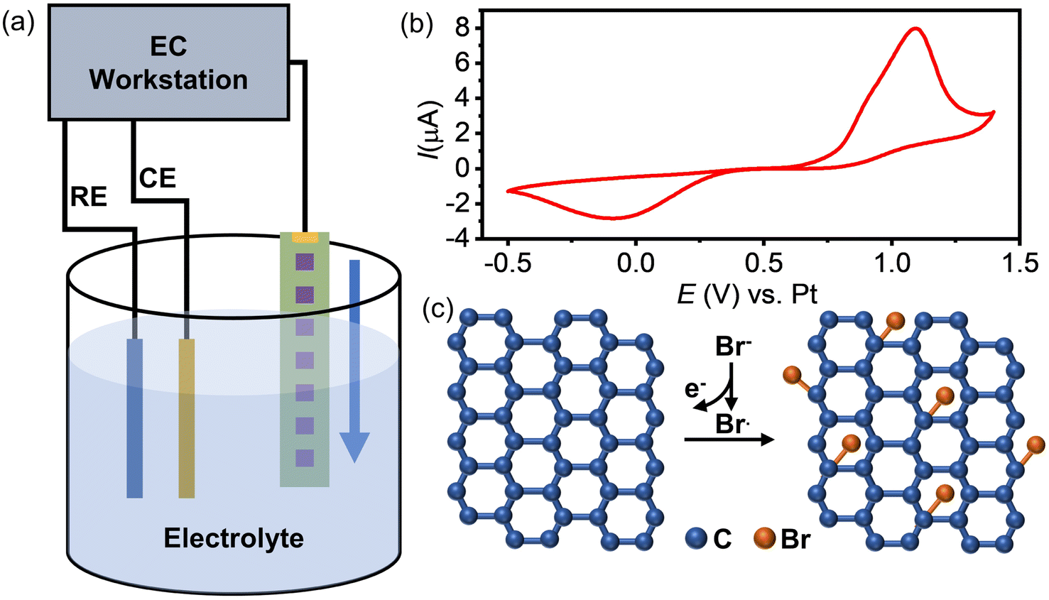 | ||
| Fig. 1 (a) Schematic diagram of the electrochemically induced bromination process. (b) A typical curve of cyclic voltammograms when the SLG substrate is employed as the working electrode in an aqueous solution with 10 mM KBr and 10 mM H2SO4; the scan rate was 100 mV s−1. (c) Schematics of the electrochemical bromination mechanism. | ||
XPS experiments were performed to identify the carbon-bromine (C–Br) functionalization of the SLG surface (ESI Fig. S1†). The results demonstrate the occurrence of an electrochemically induced brominating addition reaction and that SLG can be brominated to form brominated graphene (SLGBr). To determine the degree of bromination, Raman spectroscopy was performed to characterize the SLG samples with varying durations of CV. The results are depicted in Fig. 2a, showing good agreement with previous literature reports.39–41 For the sake of discussion, the SLG patterns were designated from A to K. The Raman spectrum of pristine SLG (spectrum A) represents a G peak at ∼1580 cm−1, a 2D peak at ∼2680 cm−1 and a 2D′ peak at ∼3247 cm−1. The presence of a symmetric 2D peak with much stronger intensity than that of the G peak confirms the graphene's single-layer nature. Moreover, the absence of the D peak (∼1345 cm−1) and D′ peak (∼1620 cm−1), which appear only in defective graphene, confirms the high quality of the graphene sample. As the bromination process proceeds, the D and D′ peaks begin to emerge and vary from pattern to pattern, indicating the introduction of sp3-C defects into graphene due to the formation of C–Br bonds. The intensity of the D peak increases from pattern B to G, followed by an intensity decrease and spectral broadening from pattern H to K. Consistent with our previous research, the structural defects introduced by C–Br bonds are supposed to be initially separated and independent, activating pristine graphene. The D peak gets stronger as the defects increase and then reaches a maximum (stage 1, shown in Fig. S3 in the ESI†). Subsequently, the “structurally disordered” areas induced by the coalescing defects would dominate in the SLG sheet, leading to a decrease in the D peak intensity (stage 2, Fig. S3 in the ESI†). The peak intensity ratio (ID/IG) is commonly utilized to characterize the defect density of graphene, which means the ratio of the sp3 to sp2 bonding character. The Raman ID/IG mapping of the graphene samples with different degrees of bromination is shown in Fig. 2b, and the corresponding average values of ID/IG are listed in Table 1.
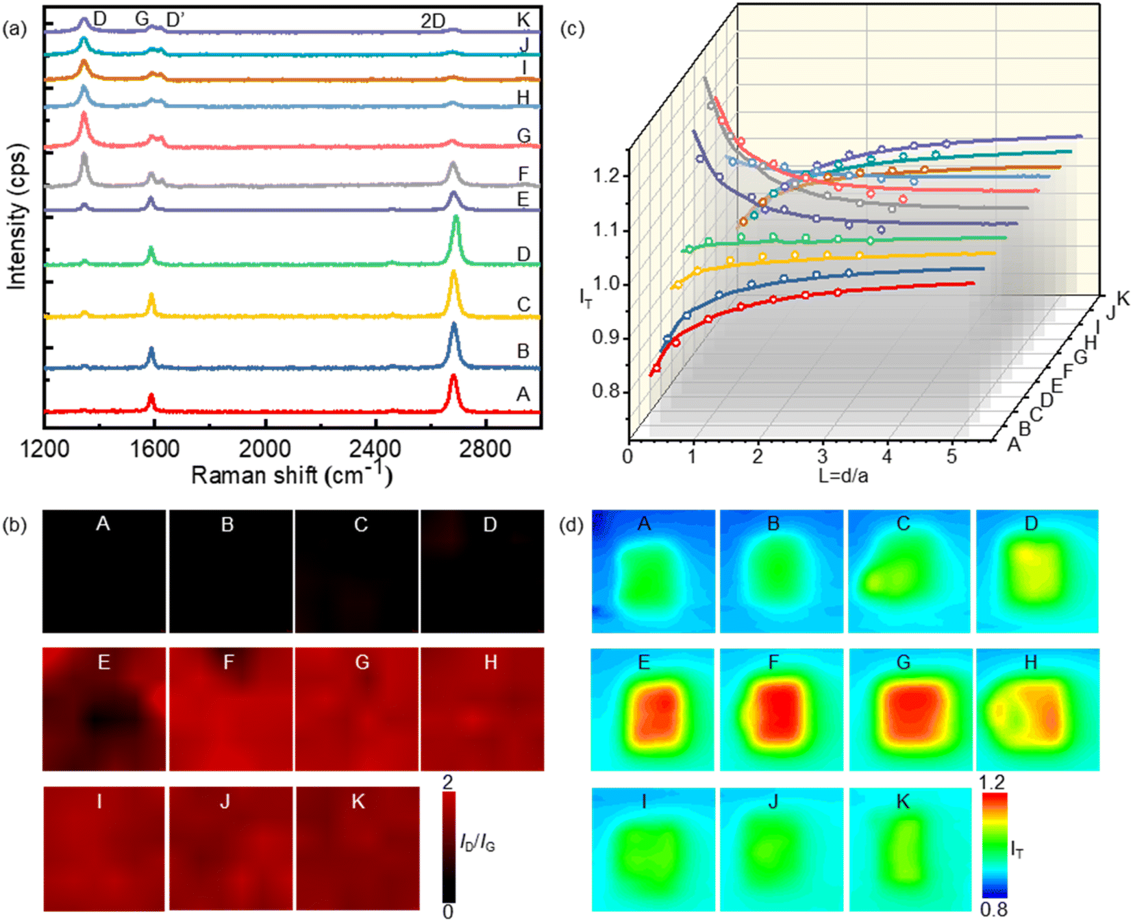 | ||
| Fig. 2 (a) Raman spectra (vertically aligned) and (b) Raman ID/IG mapping of the brominated SLG patterns. (c) The probe approaching curves and (d) SECM images obtained on the brominated SLG patterns. In the SECM experiments, the tip electrode was held at a potential of 0.4 V in the electrolyte solution containing 1 mM FcMeOH and 0.1 M KCl, while the SLG substrate was kept unbiased. The tip–substrate distance was kept constant at 2.2 µm (d/a = 0.44). | ||
| I D/IG | L D (nm) | n D (cm−2) | k 0 (cm s−1) | Label |
|---|---|---|---|---|
| — | — | — | 1.70 × 10⁻³ | 1A |
| 0.13 | 27.36 | 4.25 × 10¹⁰ | 2.20 × 10⁻³ | 1B |
| 0.15 | 25.96 | 4.73 × 10¹⁰ | 2.50 × 10⁻³ | 2A |
| 0.24 | 20.4 | 7.65 × 10¹⁰ | 3.00 × 10⁻³ | 2B |
| 0.25 | 20.2 | 7.80 × 10¹⁰ | 4.60 × 10⁻³ | 1C |
| 0.28 | 18.89 | 8.92 × 10¹⁰ | 6.50 × 10⁻³ | 1D |
| 0.51 | 13.85 | 1.66 × 10¹¹ | 2.20 × 10⁻² | 1E |
| 0.72 | 11.53 | 2.39 × 10¹¹ | 3.00 × 10⁻² | 1F |
| 1.34 | 7.95 | 5.03 × 10¹¹ | 3.50 × 10⁻² | 2C |
| 2.33 | 5.31 | 1.13 × 10¹² | 5.00 × 10⁻² | 2D |
| 2.85 | 4.24 | 1.77 × 10¹² | 6.00 × 10⁻² | 2E |
| 3.08 | 3.58 | 2.48 × 10¹² | 4.00 × 10⁻² | 1G |
| 3.07 | 2.96 | 3.64 × 10¹² | 2.50 × 10⁻² | 2F |
| 3.03 | 2.82 | 4.00 × 10¹² | 1.40 × 10⁻² | 2G |
| 2.94 | 2.67 | 4.47 × 10¹² | 1.00 × 10⁻² | 1H |
| 2.79 | 2.48 | 5.18 × 10¹² | 3.00 × 10⁻³ | 1I |
| 2.65 | 2.34 | 5.81 × 10¹² | 2.50 × 10⁻³ | 1J |
| 2.34 | 2.11 | 7.15 × 10¹² | 2.20 × 10⁻³ | 1K |
The mean distance between structural defects in graphene (LD, nm) can be determined from the intensity ratio ID/IG according to the quantitative formula expressed as follows:39
 | (1) |
 | (2) |
As shown in Fig. S2,† a specific value of ID/IG can correspond to two potential LD values. To accurately determine the true LD value, the two-stage spectral changes presented in Fig. 2a are taken into account. During stage 2, the width of the D, G, D′ and 2D peaks exhibits significant broadening (Fig. S3†), which helps in discriminating the correct LD value associated with the particular ID/IG ratio. Eventually, both LD and nD values are provided in Table 1, taking into consideration the refined LD values obtained through the two-stage spectral analysis and using the formula (eqn (1) and (2)) mentioned earlier for calculating the defect density (nD) based on the updated LD value.
SECM was employed to investigate the electrochemical activity of the SLG patterns with different durations of bromination. A Pt UME with a radius of 5 µm (r) and an RG of 2 was used as the tip electrode, while the brominated SLG was used as the substrate. FcMeOH was used as the redox couple because the outer-sphere reaction involves no specific surface interaction between FcMeOH and graphene. During the SECM measurements, the tip electrode was held at a potential of 0.45 V, while the substrate remained unbiased. The oxidized species (FcMeOH+) at the tip electrode underwent reduction to the reduced species (FcMeOH) on the SLG substrate. Subsequently, the reduced species diffused to the tip electrode and were further oxidized, forming positive feedback (see ESI Section S3 and Fig. S4† for the scheme of SECM). The feedback current of the tip is dependent on the kinetics of HET between SLG and the redox (FcMeOH); the higher the feedback current, the faster the local HET rate. The probe approaching curves and SECM imaging of the feedback current on the brominated SLG are presented in Fig. 2c and d, respectively, corresponding to Fig. 2b depicting the Raman ID/IG mapping. It is evident that as the bromination proceeds, the tip current first increases (from pattern A to G) and then decreases (pattern H to K), mirroring the variation in ID/IG. This observation indicates a clear correlation between the electrochemical activities of graphene and its defect density.
To quantitatively investigate the HET rate, the probe approaching curves were recorded. FEM modeling was employed to fit the experimental approaching curves as a function of the HET rate constant (k0) through COMSOL Multiphysics 5.5. The detailed description of the FEM modeling, including solving equations, boundary conditions, initial conditions and necessary parameters, can be found in ESI Section S4.† As depicted in Fig. 2c, the experimental approaching curves (solid lines) exhibited good agreement with the simulated results (symbols), indicating that the parameters used in the FEM modeling were reasonable and appropriate for the system under investigation. The rate constant (k0) of HET on pristine SLG was calculated to be 1.7 × 10⁻³ cm s−1 (sample A in Fig. 2b), which is lower than that reported in previous studies.21,42–44 The difference may be attributed to the variation in the processing technique of pristine CVD graphene. A perfect graphene is expected to be uniform, smooth and non-defective, thus exhibiting inert behavior in HET reactions due to its highly delocalized conjugated π system. Therefore, the lower value of k0 implies the high quality of pristine graphene. Another set of SLG patterns with different degrees of bromination was characterized by Raman spectroscopy and SECM, and the results are provided in ESI Section S5 and Fig. S7,† which also show a good correlation between them. All the obtained kinetic results (k0) are summarized in Table 1 for further systematic analysis.
Fig. 3a shows that the ID/IG value of the brominated SLG initially increased with the continuation of the bromination process and then decreased. The rate constant (k0) of HET on the brominated SLG exhibited a similar trend to the ID/IG ratio. It is essential to note that the horizontal ordinate in Fig. 3a represents the relative degree of bromination and doesn't strictly represent a proportional relationship between the results. Furthermore, it can be observed that k0 increased slightly with ID/IG at the very beginning of the bromination process and then increased to maximum rapidly, shown in Fig. 3b. After that, k0 decreased rapidly with the decrease in ID/IG and then kept stable relatively.
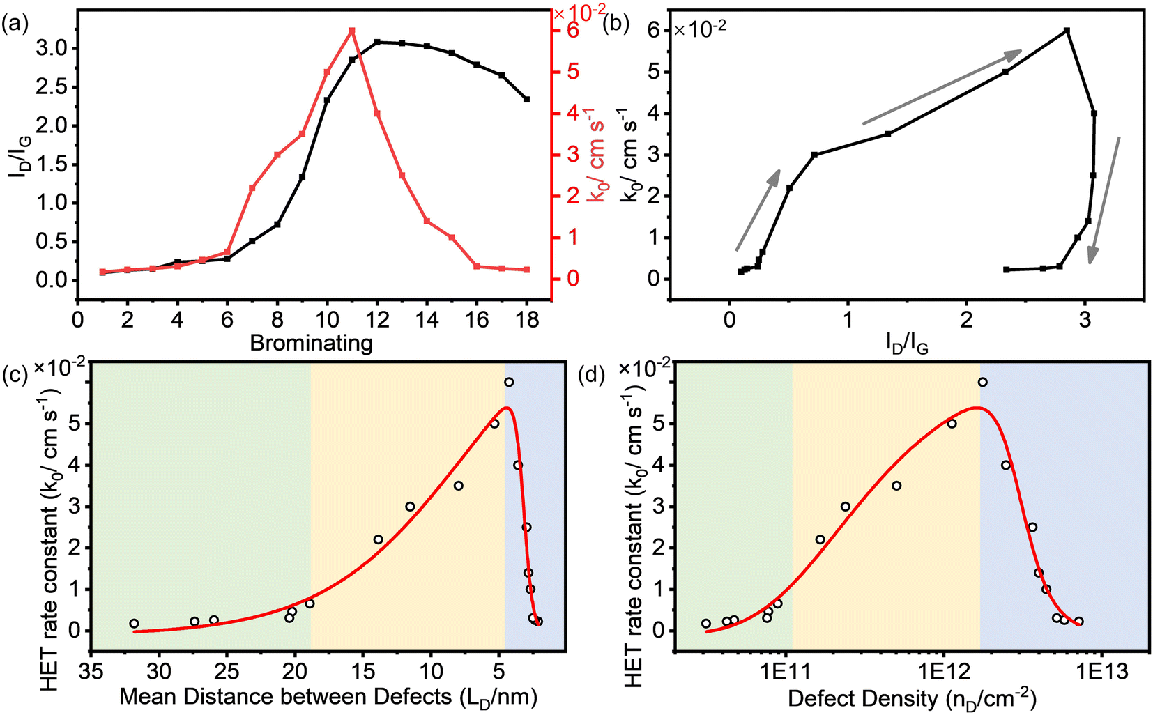 | ||
| Fig. 3 (a) The ID/IG (black line) and the standard HET rate constant k0 (red line) varying with the continuation of the bromination process. (b) The correlation between ID/IG and k0. (c and d) k0 as a function of defect density nD (cm−2) and the mean distance between defects LD (nm), respectively. | ||
The correlation between k0 and the defect parameters, including mean distance between defects (LD) and defect density (nD), is shown in Fig. 3c and d, revealing a three-region behavior. In the first region (light green in Fig. 3c), k0 increased slightly from 1.70 × 10⁻³ cm s−1 to 6.50 × 10⁻³ cm s−1 as LD decreased to 18.89 nm. Simultaneously, nD increased to 8.92 × 1010 cm−2. In this variation region, the defect density of SLG is relatively low, and its effect on the electrochemical activity of SLG is limited. As more defects were introduced, a significant enhancement of k0 from 2.20 × 10⁻² cm s−1 to 6.00 × 10⁻² cm s−1 was observed in a relatively high defect density range from 1.66 × 1011 cm−2 to 1.77 × 1012 cm−2, corresponding to LD values from ∼14.00 to ∼4.00 nm, respectively. With the defect density further increasing, the k0 decreased dramatically from 6.00 × 10⁻² cm s−1 to 2.20 × 10⁻³ cm s−1 at a defect density of 7.15 × 1012 cm−2 (LD = 2.11 nm). The enhanced electrochemical activity can be attributed to an increase in the density of states (DOS) near the Dirac point in SLG introduced by the sp3 C–Br bond, as explained in detail in our previous work.21 The introduction of defects into graphene could modulate the electronic structure of graphene and consequently enhance the HET rate.
The obtained results demonstrate a clear correlation between defect density introduced by bromination and electrochemical activity of graphene. This implies that precise control of the defect density can lead to the optimization of the electrochemical performance of graphene. Interestingly, our findings follow a similar trend of defect density dependence as observed in previous studies where point vacancy defects were introduced by Ar+ irradiation. The differences in the absolute values of the defect density (LD, nD) and k0 could be derived from the differences in surface properties of the graphene sample, because the chemical and physical properties of the graphene surface are sensitive to the fabrication method and pretreatment procedures. Nonetheless, compared to plasma irradiation techniques, the electrochemical bromination process offers a simpler and gentler approach for tailoring the defect density and consequently enhancing the electrochemical performance of graphene, making it more suitable for various electrochemical applications.
Experimental
Chemicals and materials
All chemicals used in the experiments are of analytical grade, purchased from Sinopharm Group Co. Ltd (H2SO4, KBr, KCl, acetone) and Alfa Aesar (hydroxymethyl ferrocene (FcMeOH)). A photoresist (S1805) was purchased from Merck Group. All aqueous solutions were prepared with deionized water (18.2 MΩ cm, Milli-Q, Millipore Co.).Electrochemical bromination of SLG
SLG was prepared by chemical vapor deposition (CVD, FirstNano, ET2000) on pieces of copper foil and transferred to the SiO2/Si substrate subsequently. A 500-nm-thick photoresist film (S1805) was spin-coated onto SLG and then patterned by using a laser direct writing photolithography system (Microtech LW405D, Italy) following the drying process. As a result, the exposed SLG patterns with a series of square arrays (20 µm × 20 µm) and a period of 1000 µm were obtained after exposure and development procedures. To serve as current terminals, a 10-nm-thick chrome (Cr) film and a 40-nm-thick gold (Au) film were sequentially deposited at one end of the SLG sheet sequentially by photolithography and magnetron sputtering, as depicted in Fig. 1a. For defect engineering purposes, the patterned SLG substrate, acting as the working electrode, was immersed in an aqueous electrolyte containing 10 mM KBr and 10 mM H2SO4 to perform electrochemically induced bromination by cyclic voltammetry. The potential ranged from −0.5 V to 1.4 V (vs. MSE) with a scan rate of 100 mV s−1. According to our previous study, brominated SLG would be formed due to the occurrence of an electrochemically induced brominating addition reaction, leading to an increase in defects on SLG.To mitigate errors arising from variations in pretreatment procedures and to enable reliable characterization of electrochemical activity correlated to defect density through imaging measurement, a series of SLG patterns with varying bromination degrees were prepared. Specifically, the initial pattern located at the end of the SLG substrate, far away from the current terminal, was immersed into the aqueous electrolyte. Subsequently, the substrate was incrementally moved downwards a specific distance after a certain number of CV cycles, allowing the subsequent square pattern to be exposed to the electrolyte for bromination. This process was repeated until the final pattern was brominated. Finally, the SLG patterns with different well-defined defect densities on a single piece were obtained.
Raman characterization of graphene defects
Raman measurements were performed to characterize the defects of SLG patterns on an Xplora (Horiba Jobin Yvon, France) with 532 nm laser excitation. The Raman spectra were recorded with 1200 lines per mm grating, while the laser power was kept at 5 mW with an acquisition time of 2 s.SECM characterization
All of the electrochemical measurements were performed on a CHI 920c workstation (CH Instruments Inc.). A 5-µm radius (r) Pt UME (RG = 2) was used as the SECM tip, and the as-prepared SLG substrate was used as the substrate electrode. A Pt wire and an Ag/AgCl electrode were used as the counter electrode (CE) and reference electrode (RE), respectively. The Pt UME was polished using nanoscale polishing cloth and ultrasonically cleaned in ultrapure water (Milli-Q) before experiments. The electrolyte was a solution containing 1 mM hydroxymethylferrocene (FcMeOH) and 0.1 M KCl. The probe approaching curves were recorded in feedback mode, where the tip electrode was held at 0.45 V, and the SLG substrate was unbiased. The tip–substrate distance was determined using the positive approach curves obtained with the substrate biased at 0 V (purely diffusion-controlled conditions). The SECM imaging was performed with the unbiased SLG substrate, and the tip–substrate distance was kept at 2.2 µm (L = d/a = 0.44).Finite element method (FEM) modeling
The heterogeneous electron transfer (HET) kinetics of SLG with different defect densities were derived by the finite element method (FEM) through a COMSOL Multiphysics 5.5 (COMSOL AB, Sweden) software package. The details including mass transport equations, the 2D symmetric geometry, and the boundary conditions are provided in ESI Section S4.†Conclusions
In conclusion, we have successfully developed a straightforward and controllable chemical modification method to optimize the electrochemical activity of graphene. By controllably introducing different sp3-defect densities through electrochemical bromination, we were able to enhance the electrochemical activity of SLG. Raman spectroscopy and scanning electrochemical microscopy were utilized to investigate the correlation between the HET rate and sp3-defect density of SLG. The results indicate that the electrochemical activity of SLG is improved at a moderate defect density and then decreases at high defect density. The research demonstrates that the electrochemical activity of SLG can be precisely tuned by introducing different sp3-defect densities through electrochemical bromination under ambient conditions. This approach offers a controllable, effective, and environmentally friendly method to optimize the electrochemical activity of graphene, making it more suitable for a wide range of electrochemical applications.Data availability
The authors declare that all data supporting the findings of this study are available from the corresponding author upon reasonable request.Author contributions
L. Zeng, L. Han, W. Nan, and J. Su: electrochemical experiments and instrumental characterization; L. Zeng, W. Song, S. Luo, and Y. Wu: microfabrication and electronic characterization; L. Zeng and L. Han: theoretical discussions; D. Zhan: originated, designed and organized the work and wrote the manuscript; all the authors participated in the discussions and preparation of the manuscript.Conflicts of interest
There are no conflicts to declare.Acknowledgements
The financial support of the National Natural Science Foundation of China (22202166, 21827802, 22132003 and 22021001), Fundamental Research Funds for the Central Universities (20720230076) and the 111 Project (B08027 and B17027) is appreciated. The authors declare no competing financial interests.Notes and references
- S. V. Morozov, K. S. Novoselov, M. I. Katsnelson, F. Schedin, D. C. Elias, J. A. Jaszczak and A. K. Geim, Phys. Rev. Lett., 2008, 100, 016602 CrossRef CAS PubMed.
- R. R. Nair, P. Blake, A. N. Grigorenko, K. S. Novoselov, T. J. Booth, T. Stauber, N. M. R. Peres and A. K. Geim, Science, 2008, 320, 1308 CrossRef CAS PubMed.
- A. K. Geim, Science, 2009, 324, 1530–1534 CrossRef CAS PubMed.
- Y. Xiao, Y. Su, X. Liu and W. Xu, J. Phys. Chem. Lett., 2019, 10, 5402–5407 CrossRef CAS PubMed.
- M. Pumera, Chem. Soc. Rev., 2010, 39, 4146–4157 RSC.
- M. Vaqueiro-Contreras, C. Bartlam, R. S. Bonilla, V. P. Markevich, M. P. Halsall, A. Vijayaraghavan and A. R. Peaker, Sol. Energy Mater. Sol. Cells, 2018, 187, 189–193 CrossRef CAS.
- Y. Han, X. Yan, Q. Wu, H. Xu, Q. Li, A. Du and X. Yao, Small Struct., 2023, 4, 2300036 CrossRef.
- J. Zhu and S. Mu, Adv. Funct. Mater., 2020, 30, 2001097 CrossRef CAS.
- E. Santos, R. Nazmutdinov and W. Schmickler, Curr. Opin. Electrochem., 2020, 19, 106–112 CrossRef CAS.
- A. K. Verma, A. M. Verma and A. Govind Rajan, Curr. Opin. Electrochem., 2022, 36, 101116 CrossRef CAS.
- X. Yan, Y. Jia and X. Yao, Chem. Soc. Rev., 2018, 47, 7628–7658 RSC.
- Y. Jia, J. Chen and X. Yao, Mater. Chem. Front., 2018, 2, 1250–1268 RSC.
- M. López-Suárez, F. Torres, N. Mestres, R. Rurali and G. Abadal, Microelectron. Eng., 2014, 129, 81–85 CrossRef.
- M. F. El-Kady, V. Strong, S. Dubin and R. B. Kaner, Science, 2012, 335, 1326–1330 CrossRef CAS PubMed.
- C. K. Chua, Z. Sofer, B. Khezri, R. D. Webster and M. Pumera, Phys. Chem. Chem. Phys., 2016, 18, 17875–17880 RSC.
- X. L. Li, X. R. Wang, L. Zhang, S. W. Lee and H. J. Dai, Science, 2008, 319, 1229–1232 CrossRef CAS PubMed.
- Y. B. Fu, H. Yang, Y. X. Gao, L. Huang, R. Berger, J. Z. Liu, H. L. Lu, Z. H. Cheng, S. X. Du, H. J. Gao and X. L. Feng, Angew. Chem., Int. Ed., 2020, 59, 8873–8879 CrossRef CAS PubMed.
- A. Narita, X.-Y. Wang, X. Feng and K. Müllen, Chem. Soc. Rev., 2015, 44, 6616–6643 RSC.
- A. W. Robertson, C. S. Allen, Y. A. Wu, K. He, J. Olivier, J. Neethling, A. I. Kirkland and J. H. Warner, Nat. Commun., 2012, 3, 1144 CrossRef PubMed.
- X. R. Wang and H. J. Dai, Nat. Chem., 2010, 2, 661–665 CrossRef CAS PubMed.
- J.-H. Zhong, J. Zhang, X. Jin, J.-Y. Liu, Q. Li, M.-H. Li, W. Cai, D.-Y. Wu, D. Zhan and B. Ren, J. Am. Chem. Soc., 2014, 136, 16609–16617 CrossRef CAS PubMed.
- L. Tao, Q. Wang, S. Dou, Z. Ma, J. Huo, S. Wang and L. Dai, Chem. Commun., 2016, 52, 2764–2767 RSC.
- Q. Wang, Y. Lei, D. Wang and Y. Li, Energy Environ. Sci., 2019, 12, 1730–1750 RSC.
- E. Y. Andrei and A. H. MacDonald, Nat. Mater., 2020, 19, 1265–1275 CrossRef CAS PubMed.
- D.-Y. Yeom, W. Jeon, N. D. K. Tu, S. Y. Yeo, S.-S. Lee, B. J. Sung, H. Chang, J. A. Lim and H. Kim, Sci. Rep., 2015, 5, 9817 CrossRef CAS PubMed.
- M. Rybin, A. Pereyaslavtsev, T. Vasilieva, V. Myasnikov, I. Sokolov, A. Pavlova, E. Obraztsova, A. Khomich, V. Ralchenko and E. Obraztsova, Carbon, 2016, 96, 196–202 CrossRef CAS.
- Z. H. Sheng, H. L. Gao, W. J. Bao, F. B. Wang and X. H. Xia, J. Mater. Chem., 2012, 22, 390–395 RSC.
- Y. Wang, Y. Y. Shao, D. W. Matson, J. H. Li and Y. H. Lin, ACS Nano, 2010, 4, 1790–1798 CrossRef CAS PubMed.
- L. Chen, J. Han, Y. Ito, T. Fujita, G. Huang, K. Hu, A. Hirata, K. Watanabe and M. Chen, Angew. Chem., Int. Ed., 2018, 57, 13302–13307 CrossRef CAS PubMed.
- Q. Wang, Y. Ji, Y. Lei, Y. Wang, Y. Wang, Y. Li and S. Wang, ACS Energy Lett., 2018, 3, 1183–1191 CrossRef CAS.
- S. Boopathi, T. N. Narayanan and S. S. Kumar, Nanoscale, 2014, 6, 10140–10146 RSC.
- F. Zhou, H. Huang, C. Xiao, S. Zheng, X. Shi, J. Qin, Q. Fu, X. Bao, X. Feng, K. Müllen and Z.-S. Wu, J. Am. Chem. Soc., 2018, 140, 8198–8205 CrossRef CAS.
- W. Li, Y. Li and K. Xu, Nano Lett., 2021, 21, 1150–1155 CrossRef CAS PubMed.
- C. Wetzl, A. Silvestri, M. Garrido, H.-L. Hou, A. Criado and M. Prato, Angew. Chem., Int. Ed., 2023, 62, e202212857 CrossRef CAS PubMed.
- K. C. Knirsch, R. A. Schäfer, F. Hauke and A. Hirsch, Angew. Chem., Int. Ed., 2016, 55, 5861–5864 CrossRef CAS PubMed.
- Y. Xia, C. Martin, J. Seibel, S. Eyley, W. Thielemans, M. van der Auweraer, K. S. Mali and S. De Feyter, Nanoscale, 2020, 12, 11916–11926 RSC.
- J. Li, M. Li, L.-L. Zhou, S.-Y. Lang, H.-Y. Lu, D. Wang, C.-F. Chen and L.-J. Wan, J. Am. Chem. Soc., 2016, 138, 7448–7451 CrossRef CAS PubMed.
- L. Zeng, W. Song, X. Jin, Q. He, L. Han, Y.-f. Wu, C. Lagrost, Y. Leroux, P. Hapiot, Y. Cao, J. Cheng and D. Zhan, Chem. Sci., 2023, 14, 4500–4505 RSC.
- M. M. Lucchese, F. Stavale, E. H. M. Ferreira, C. Vilani, M. V. O. Moutinho, R. B. Capaz, C. A. Achete and A. Jorio, Carbon, 2010, 48, 1592–1597 CrossRef CAS.
- A. Eckmann, A. Felten, I. Verzhbitskiy, R. Davey and C. Casiraghi, Phys. Rev. B: Condens. Matter Mater. Phys., 2013, 88, 035426 CrossRef.
- L. G. Cancado, A. Jorio, E. H. M. Ferreira, F. Stavale, C. A. Achete, R. B. Capaz, M. V. O. Moutinho, A. Lombardo, T. S. Kulmala and A. C. Ferrari, Nano Lett., 2011, 11, 3190–3196 CrossRef CAS PubMed.
- J. Zhang, J. Guo, D. Chen, J.-H. Zhong, J.-Y. Liu and D. Zhan, Appl. Surf. Sci., 2019, 491, 553–559 CrossRef CAS.
- W. Li, C. Tan, M. A. Lowe, H. D. Abruña and D. C. Ralph, ACS Nano, 2011, 5, 2264–2270 CrossRef CAS PubMed.
- N. L. Ritzert, J. Rodriguez-Lopez, C. Tan and H. D. Abruna, Langmuir, 2013, 29, 1683–1694 CrossRef CAS PubMed.
Footnote |
| † Electronic supplementary information (ESI) available. See DOI: https://doi.org/10.1039/d3sc03920j |
| This journal is © The Royal Society of Chemistry 2024 |