DOI:
10.1039/D4RA04344H
(Paper)
RSC Adv., 2024,
14, 28401-28414
Direct vapour transport grown Cu2SnS3 crystals: exploring structural, elastic, optical, and electronic properties
Received
13th June 2024
, Accepted 7th August 2024
First published on 5th September 2024
Abstract
Copper tin sulphide (Cu2SnS3) (CTS) has emerged as a potent material for applications in photovoltaic, thermoelectric, electrochemical, biological, and other fields. CTS has superior properties such as non-toxicity, direct bandgap, p-type conductivity, variable crystal structure, alterable morphology and ease of synthesis, and it is a better substitute for conventional semiconductor materials. In the present work, CTS crystals were grown using direct vapour transport. Investigation through X-ray diffraction showed that the as-grown CTS crystals possessed a cubic unit cell structure with a = b = c = 5.403 Å. The analysis of the binding energies and composition of constituents of the as-grown CTS crystals via X-ray photoelectron spectroscopy confirmed the presence of Cu1+, Sn4+ and S2−. The experimental bandgap of CTS crystals is 1.23 eV, which was confirmed by diffuse reflectance spectroscopy. The investigation of elastic, optical, thermal and electronic properties of CTS crystals was carried out via density functional theory employing generalized gradient approximation with the Perdew−Burke–Ernzerhof exchange-relationship functional. The first-ever analysis of the temperature-dependent elastic properties of CTS crystals revealed greater stability at elevated temperature (953 K). Dielectric properties, reflectivity, refractive index, loss function, extinction and absorption coefficients of CTS crystals were computed and analyzed in detail. The evaluation of the electronic band structure with density of states revealed valence band maximum and conduction band energy level contributions, showing a bandgap of 1.2 eV. The obtained results are discussed in detail.
1. Introduction
Nowadays, transition metal chalcogenides (TMCs) epitomize cutting-edge advancements, showcasing a spectrum of benefits, from facilitating experimental and theoretical property simulations to delivering tailor-made applications. TMCs possess remarkable characteristics such as the ability to provide excellent capacity in storage devices;1 faster and efficient degradation of harmful dyes via photocatalysis;2 attractive bandgap range;3 high responsivity, detectivity, and external quantum efficiency in the case of visible, infrared, and ultra-violet photodetectors;4,5 significant antibacterial, antioxidant, and cytotoxicity in biological applications;6,7 and significant gas sensing in the case of sensing various pollutants such as CO2, NO2, and SO2.8 Theoretical investigation by applying the density functional theory (DFT) approach and simulations based on different properties such as optical, structural, elastic, electronic, and thermoelectric, can deliver impressive outcomes.9 Various functions, such as plane wave and atom-centered free DFT, are utilized for simulations of different ground state properties and advanced theoretical characterizations.10,11 Copper-based ternary chalcogenides are gaining prominence owing to their simplicity in synthesis, cost-effective production, significant yield and versatility in tailoring properties to meet specific experimental and theoretical requirements. Cu2SnS3 (CTS) has garnered significant attention and widespread research focus, thus establishing itself as a key compound among other copper-based ternary chalcogenides.12–21 CTS belongs to the I–IV–VI group, which possesses other secondary phases such as Cu3SnS4, Cu3SnS7, Cu4SnS7, and Cu5SnS7. Among all the other counter phases, CTS possesses superior properties, such as p-type conductivity;22 an attractive span of bandgap (0.93–1.75 eV);23 elevated ZT and Seebeck coefficient values;24 high absorption coefficient and charge carrier concentration;25 significant thermal stability;26 and the existence of various phases such as cubic, tetragonal, monoclinic, and triclinic.27 CTS can be synthesized in nano to bulk form by various physical and chemical methods. The CTS in nano-forms is synthesized by several methods, such as solvothermal,28 hydrothermal,29 one pot chemical,30 hot injection,31 and ball milling.32 These CTS-based nano-forms have various applications, such as in storage devices,32 photocatalyst and hydrogen evolution,33,34 potent antimicrobial agents,35 and hole transporting material in solar cells.36 CTS has been deposited in thin-film form using various physical and chemical routes, such as sputtering,37 spray pyrolysis,38 evaporation,39 pulsed laser deposition,40 electrodeposition,41 chemical bath deposition,42 spin coating,43 dip coating,44 and doctor blade.45 The CTS in thin-film forms performs excellently in photovoltaics, photodetectors, and sensors.46–48 The literature review reveals numerous studies dedicated to the exploration of CTS in both nano- and thin-film forms, showcasing in-depth experimental and theoretical frameworks based on the structure, optical, thermoelectric, electric and dielectric traits of CTS.49 There are very few reports on CTS crystal growth and characterization. Matsumoto et al.,50 Raval et al.51 and Kim et al.52 grew CTS crystals by chemical vapour transport (CVT), direct vapour transport (DVT) and Bridgman techniques, respectively. They investigated the effects of iodine concentration, thermal and electrical transport properties, and pressure on the growth of the CTS crystal. There are few reports on CTS crystal growth and characterization using various methods. Regarding the theoretical framework, analysis of the diverse ground state properties of CTS crystals has not yet been reported.
In the present study, the authors performed CTS crystal growth by applying the DVT method. The as-grown CTS crystals are characterized by their structure, composition, and optical properties. The thermal behaviour of the as-grown CTS crystal is carried out by thermogravimetric (TG), differential thermogravimetric (DTG) and differential thermal analysis (DTA) techniques. The thermal plots are recorded in an inert nitrogen (N2) gas atmosphere in a temperature range of 305–1113 K. To the best of our knowledge, the literature reveals no investigation on DVT-grown CTS crystals of the theoretical correlation between mechanical and thermal characteristics. In response to this gap, the authors investigated temperature-dependent elastic properties, the energy band and structural stability, as well as optical and dielectric characteristics of CTS. The authors used ion charge theory to investigate the elastic characteristics of CTS crystals. This work mainly focuses on the utilization of the density functional theory (DFT) framework in understanding the mechanical, optical, and electronic properties of CTS crystals. A thorough examination of the thermo-elastic properties of CTS crystals is carried out based on thermal analysis. We perform two simulations: investigation of elastic properties of grown CTS crystals at room temperature (310 K) and at 953 K. In-depth DFT analysis is extended to understand the electronic, dielectric and optical properties of the CTS crystals.
2. Experiment
The crystals of CTS are grown by applying the DVT technique. At the start of the typical growth process, compound CTS is synthesized using pure elemental copper (Cu) [minimum assay 99.999%, Alpha Aesar, USA], tin (Sn) [minimum assay 99.5%, CDH, India] and sulphur (S) [minimum assay 99.5%, Alpha Aesar, USA]. All the precursor constituents (Cu, Sn and S) are taken as 2.97, 2.77 and 2.25 gm, respectively, and sealed in an acid-cleaned dried ampoule made of quartz under a vacuum of ∼10−5 torr. The employed quartz ampoule has a length and inner diameter of 22 cm and 2 cm, respectively. The vacuum-sealed quartz ampoule is loaded in a horizontal furnace for the compound preparation. In this compound preparation, the elemental mixture is spread evenly all over the ampoule length. The furnace is programmed to achieve a set temperature of 1173 K in 24 h. The ampoule is held at this temperature for 48 h. On completion of the run, the ampoule is cooled to an ambient temperature. The prepared compound is retrieved by the physical breaking of the ampoule. The compound is powdered and transferred to another clean ampoule and vacuum sealed. The entire powder compound is made to be at one end of the ampoule called charge end and another empty ampoule end is called growth end. Under this condition, the ampoule is put into a two-zone furnace for CTS single crystal growth. The furnace zone with the charge ampoule end is 1173 K, and the empty ampoule growth end furnace zone is 1123 K with a controlled heating rate of 25 K h−1. The single crystal growth occurs under this temperature gradient condition for 90 h. After crystal growth run completion, the ampoule is cooled to ambient temperature with a very slow cooling rate of 10 K h−1. Slow cooling is performed to avoid thermal cracks in the as-grown crystals. The shiny gray CTS crystals are removed by the physical breaking of the ampoule. Fig. 1 shows a schematic diagram of the entire growth process and a photograph of the as-grown crystals.
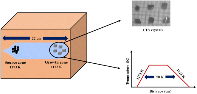 |
| | Fig. 1 Schematic of CTS growth conditions and as-grown crystals using the DVT method. | |
3. Characterizations
The phase of as-grown CTS crystals is confirmed by powder X-ray diffraction (XRD) using a Rigaku Ultima IV powder X-ray diffractometer. The oxidation states, binding energy, and composition of as-grown CTS crystals are determined by X-ray photoelectron spectroscopy (XPS) employing a Thermofisher Scientific Instrument. The optical study of as-grown CTS crystals is performed by employing diffuse reflectance spectroscopy (DRS) using Lambda 19, PerkinElmer, USA. The thermal study of as-grown CTS crystals is analysed using a thermal analyser, Seiko SII-EXSTAR TG/DTA-7200. In thermal analysis, the curves of TG, DTG and DTA are measured concurrently in an inert atmosphere of nitrogen (N2) gas in the span of temperature from 305 K to 1113 K.
4. Computational details
The elastic, optical, thermal, and electronic properties of CTS crystals are determined by DFT using the Quantum Espresso (PWSCF) simulation package.53 Computation of the bulk electronic properties of CTS crystals is performed by considering the structure as a cubic unit cell with lattice parameters of a = b = c = 5.403 Å, with 36 atoms in its supercell. The generalized gradient approximation (GGA) with Perdew–Burke–Ernzerhof (PBE) exchange-correlation function is employed considering relaxation of ions in the crystal structure and determining the overall energy of the CTS bulk supercells.9,24,54 The electrical structure of these bulk supercells is computed using the PBE screened function.55 The GGA function provides a more precise prediction of the bandgap and the electronic structure, which are in good match with experimental data.56,57 The combination of DFT simulations and the GGA function stands out because of its ability to provide highly accurate predictions of electronic structures. First, ion and cell relaxation is performed using GGA, followed by computation of CTS crystal using PBE type pseudopotentials.58–60 This is performed by freezing the core electron (i.e. Cu: 1s2 2s2 2p6 3s2 3p6; Sn: 1s2 2s2 2p6 3s2 3p6 3d10 4s2 4p6; S: 1s2 2s2 2p6 are treated as part of frozen core) and substituting the abrupt electron density variations associated with core electrons with a more gradual and smoothed density distribution.61 The valence electron configurations are performed using 3d10 4s1 Cu electrons, 4d10 5s2 5p2 Sn electrons, and 3s2 3p4 S electrons. This configuration lacks unpaired electrons, indicating a non-magnetic nature,62 as Cu2+ and S2− ions typically form closed-shell electronic structures. Convergence experiments are performed to identify the k-point meshes (for Brillouin zone integration) and cut-off energy (for plane wave expansion).63 The Brillouin zone integration for the bulk CTS supercell is carried out utilizing Monkhorst–Pack k-point meshes with 12 × 12 × 12 k-point grid. A cut-off energy of 700 eV is applied in the expansion of the plane wave. The authors expanded the potentials and charge density within muffin-tin spheres by incorporating spherical harmonics with an lmax of 7, coupled with non-spherical components with an lmax of 6. In the process of denoting the potentials and charge densities, the authors employed Fourier series in the interstitial region. To achieve self-consistency in these computations, the irreducible Brillouin zone is set to k-points = 700. The optical traits are derived using the imaginary component of the complex dielectric function using the following equation:64| |
 | (1) |
where Ω represents the basic cell volume; ν and c represent the valence and conduction bands, respectively; ω represents the received light frequency and k represents the polarization direction of the electric field in polycrystalline materials with a complete isotropic average value. In this work, the authors estimated optical characteristics such as reflectivity R(ω), absorption coefficient I(ω), refractive indices n(ω), energy-loss spectrum L(ω), extinction coefficient k(ω), and real optical conductivity σreal(ω) by utilizing the following equations:65,66| |
 | (2) |
| |
 | (3) |
| |
 | (4) |
| |
 | (5) |
| |
 | (6) |
| | |
σreal(ω) = ε0(ω)ε1(ω).
| (7) |
5. Results and discussions
5.1 XRD
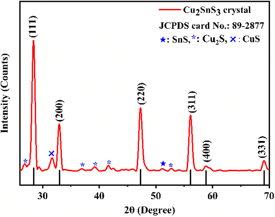
Fig. 2 depicts the powder XRD pattern of the as-grown CTS crystals along with standard JCPDS data. The crystal lattice demonstrates cubic unit cell structure with minor SnS, Cu2S and CuS secondary phases.67 The as-grown CTS crystal possesses preferential growth along the (111), (200), (220), (311), (400), and (331) planes, each positioned at different 2θ angles. Table 1 shows the calculated lattice parameters of the as-grown CTS crystals from the XRD pattern.
 |
| | Fig. 2 XRD pattern of the as-grown CTS crystals. | |
Table 1 Structural parameters of the as-grown CTS crystals calculated from the XRD pattern
| 2θ (Degree) |
Crystallite size (D) (nm) |
(hkl) |
d-spacing (Å) |
| Observed |
Calculated |
% error |
| 28.43 |
28.59 |
0.55 |
7.94 |
(111) |
3.13 |
| 32.95 |
33.13 |
0.54 |
8.03 |
(200) |
2.71 |
| 47.29 |
47.56 |
0.56 |
8.40 |
(220) |
1.92 |
| 56.10 |
56.43 |
0.58 |
8.72 |
(311) |
1.63 |
| 69.08 |
69.53 |
0.64 |
9.35 |
(400) |
1.35 |
| 76.42 |
76.84 |
0.54 |
9.80 |
(331) |
1.24 |
The average crystallite size of the as-grown CTS crystal is calculated by employing standard Scherrer's formula51 given by
| |
 | (8) |
where
λ is the wavelength of the Cu-K
α X-ray radiation (1.5408 Å), K is the structure parameter taken as 0.94,
β is full width at half maximum and
θ is Bragg's angle. The average crystallite size in the CTS crystal calculated from
eqn (8) is 8.70 nm. The
d-spacing of the as-grown CTS crystal is calculated by employing the following standard equation for the cubic crystal system,
68| |
 | (9) |
where
d is the spacing between crystallographic planes in Å;
h,
k and
l are the miller indices; and
a is the lattice parameter in Å which is 5.403 Å.
5.2 XPS
The observed spectrum of XPS shown in Fig. 3(a) of the as-grown CTS crystals provides conclusive evidence of its chemical composition, exhibiting distinct peaks corresponding to Cu, Sn, S and O. The individual XPS spectra of Cu 2p, Sn 3d and S 2p are shown in Fig. 3(b)–(d), respectively.
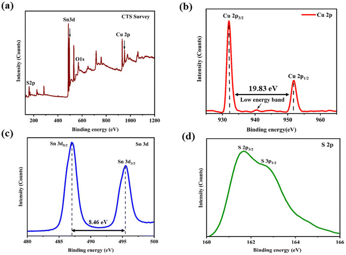 |
| | Fig. 3 XPS profile of the CTS crystal: (a) full spectrum, (b) Cu 2p, (c) Sn 3d, and (d) S 2p. | |
The XPS spectrum of the core level for Cu 2p (Fig. 3(b)) shows the presence of two different peaks with binding energies of 931.94 and 951.77 eV, corresponding to 2p3/2 and 2p1/2, respectively. Additionally, a small low-energy band is observed at 940.56 eV due to minor absorption of oxygen on the surface.69,70 The XPS spectrum of the core level for Sn 3d is shown in Fig. 3(c). It shows two peaks with binding energies of 487.03 and 495.46 eV attributed to 3d5/2 and 3d3/2, respectively. The core level XPS spectrum of S 2p is shown in Fig. 3(d). There are two peaks with binding energies of 161.65 and 162.62 eV designated to 2p3/2 and 2p1/2, respectively. The XPS profiles depict the formation of pristine and near stoichiometric compositions of the as-grown CTS crystals.
5.3 DRS
The diffuse reflectance spectrum of the as-grown CTS crystals is depicted in Fig. 4(a). The identification of an absorption edge around 632.44 nm signifies visible range absorption by as-grown CTS crystals. Fig. 4(b) shows the plot of Tauc's with Kubelka–Munk (K–M) function.
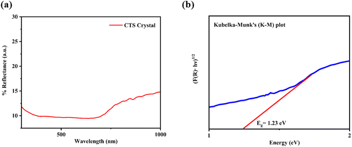 |
| | Fig. 4 (a) Diffuse reflectance spectrum and (b) K–M plot of CTS crystals. | |
The bandgap of CTS crystals is determined using standard Tauc's equation:2
| | |
(F(R)·hυ)1/n = A(Eg − hυ),
| (10) |
where
F(
R) is the Kubelka–Munk (K–M) function, hν is energy of photon and
n is taken as 2.
The estimated direct optical bandgap from the plot of (F(R)·hυ)1/2 versus energy is 1.23 eV. This direct optical bandgap value is in good match with the reported bandgap range of 0.93–1.75 eV.71
5.4 Thermal analysis
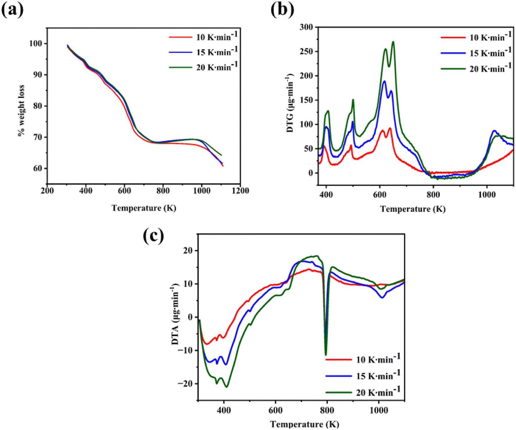
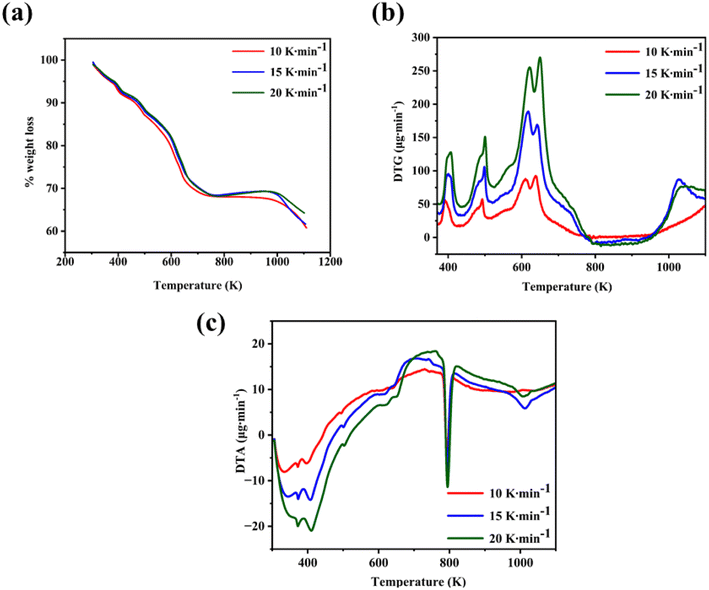
A thermal study of the as-grown CTS crystals is carried out by recording the curves of TG, DTG, and DTA. The curves are traced for three heating rates of 10, 15, and 20 K min−1. These temperature-dependent curves are precisely measured in an inert N2 atmosphere, in the range of 305 K to 1113 K. The initial sample weight taken for the thermal analyses ranges from 5 to 7 mg.
The TG and DTG curves of the as-grown CTS crystal are shown in Fig. 5(a) and (b), respectively. The TG curve in Fig. 5(a) clearly shows four-step weight losses in the temperature ranging from 305 to 1113 K for the three rates of heating of 10, 15, and 20 K min−1. The four-step decomposition is confirmed by the DTG curve (Fig. 5(b)). The DTG curves show four prominent peaks, stating four-step thermal decompositions.
 |
| | Fig. 5 (a) TG, (b) DTG, and (c) DTA of the CTS as-grown crystals. | |
The details of temperature ranges, percentage weight losses in each step, and DTG peak details are presented in Table 2.
Table 2 Thermal parameters calculated from the thermocurves
| Steps |
Temperature range (K) |
% average weight loss |
DTG |
| Heating rate (K min−1) |
Peak position |
| 10 |
15 |
20 |
Temperature (K) |
(µg min−1) |
| 1 |
305.00–418.65 |
6.84 |
405.15 |
125.72 |
| 2 |
418.65–505.51 |
5.74 |
499.48 |
147.15 |
| 3 |
505.51–753.57 |
17.84 |
636.05 |
259.71 |
| 4 |
1000.00–1107.20 |
2.23 |
1029.43 |
86.18 |
Step – 1 shows a progressive weight loss of 6.84% occurring in a temperature range of 305–418.65 K. Weight loss occurs by the evaporation of water molecules, indicating surface moisture or hydration effects within the CTS crystal lattice. After the initial phase, a subsequent weight loss of 5.74% occurs in a temperature range of 418.65–505.51 K. This weight loss temperature range is stated in Step – 2. The weight loss occurs due to the release of loosely bound atoms and molecules, indicating structural reorganization in the CTS crystal lattice.72,73 In comparison to the modest weight losses witnessed in Steps – 1 and 2, a substantial weight loss of 17.84% occurs in Step – 3 between 505.51 and 753.57 K. This prominent weight loss is mainly attributed to the decomposition of CTS between the mentioned temperature range and the major amount of sulphur loss in this temperature range.72,73 In the temperature range of 753.57 K to 1000 K, there is no weight loss in the sample. This stable region demonstrates pristine crystalline CTS formation. After the stable temperature region, a minor weight loss of 2.23% is observed in the temperature range of 1000–1107.20 K shown in Step – 4. In this high-temperature range of Step – 4, the thermal putrefaction of CTS starts. Fig. 5(b) illustrates the DTG plots of CTS crystals for three rates of heating of 10, 15, and 20 K min−1. It reveals four distinct peaks, stating the loss of weight by four steps. The weight loss peak positions align with the temperature intervals outlined for each decomposition TG step. This observation reconfirms the four steps of decomposition of the as-grown CTS crystals. Fig. 5(c) shows the DTA plots of the as-grown CTS crystals. The curves illustrate the initial endothermic nature, followed by the exothermic nature. In the later exothermic nature, a sharp endothermic peak is observed at nearly 790 K. This endothermic peak occurs due to a structural phase change in CTS.74,75 Fig. 6 shows the powder XRD patterns of the CTS crystal vacuum annealed at 753 K, 853 K and 1000 K to check the crystallinity of the CTS crystal.
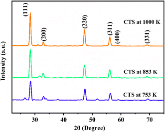 |
| | Fig. 6 XRD pattern of CTS crystal at 753, 853 and 1000 K. | |
The analysis in Fig. 6 shows an increase in intensity and sharpness of the prominent XRD peaks of CTS as temperature increases from 753 K and 853 K to 1000 K. This sharpness is attributed to the formation of pristine CTS crystals. Compared to the as-grown CTS crystal (Fig. 2), crystallinity is improved as the annealing temperature increases. The intensity of all the secondary phases in CTS is reduced under the effect of annealing temperature. This thermal study provides an in-depth understanding of how CTS crystals behave in the temperature range of ambient to 1113 K. This understanding will help in the application of CTS crystals at high temperatures in future efficacy.
6. Theoretical simulations of structural, elastic, optical and electronic properties of CTS crystals
6.1 Structural properties of CTS crystals
The CTS is a beta indium sulphide-derived structure and crystallizes in the cubic ![[F with combining macron]](https://www.rsc.org/images/entities/i_char_0046_0304.gif) 43m space group and non-magnetic crystal. Cu1+ is bonded to four equivalent S2− atoms to form CuS4 tetrahedra that share corners with twelve equivalent SnS6 octahedra. Fig. 7(a) and (b) show the representation of the unit cell and 3D crystal structure of the CTS crystal, respectively. The tilt angles of the corner-sharing octahedral are 57°. The measured bond length for all Cu–S bonds is 2.33 Å. The Sn4+ is bonded to six S2− atoms to become SnS6 octahedra that share corners with three equivalent CuS4 tetrahedra and edges with six equivalent SnS6 octahedra. In this structure, Sn–S with two bond lengths is measured: three shorter (2.60 Å) and three longer (2.67 Å). There are two inequivalent S2− sites. In the first, it is bonded in a distorted rectangular see-saw-like geometry to one Cu1+ and three equivalent Sn4+ atoms. In the second, the S2− is bonded in a distorted T-shaped geometry to three equivalent Sn4+ atoms.
43m space group and non-magnetic crystal. Cu1+ is bonded to four equivalent S2− atoms to form CuS4 tetrahedra that share corners with twelve equivalent SnS6 octahedra. Fig. 7(a) and (b) show the representation of the unit cell and 3D crystal structure of the CTS crystal, respectively. The tilt angles of the corner-sharing octahedral are 57°. The measured bond length for all Cu–S bonds is 2.33 Å. The Sn4+ is bonded to six S2− atoms to become SnS6 octahedra that share corners with three equivalent CuS4 tetrahedra and edges with six equivalent SnS6 octahedra. In this structure, Sn–S with two bond lengths is measured: three shorter (2.60 Å) and three longer (2.67 Å). There are two inequivalent S2− sites. In the first, it is bonded in a distorted rectangular see-saw-like geometry to one Cu1+ and three equivalent Sn4+ atoms. In the second, the S2− is bonded in a distorted T-shaped geometry to three equivalent Sn4+ atoms.
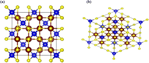 |
| | Fig. 7 (a) Representation of unit cells of the cubic CTS crystal, and (b) 3D crystal structure of the CTS crystal, with Cu (brown), Sn (blue) and S (yellow). | |
6.2 Evaluation of the temperature-dependent elastic properties of CTS crystals
This study aims to comprehensively analyze the variations in elastic constants, including Young's modulus, shear modulus, and Poisson's ratio, of CTS crystals at two distinct temperatures, 310 K and 953 K. An experimental study of the elastic properties of CTS is reported, where experimental techniques such as nano-indentation and acoustic microscopy are employed to measure the mechanical properties of CTS crystals subjected to varying temperature conditions.76,77 The present comparative analysis at two distinct temperatures of 310 K and 953 K sheds light on the material's thermal stability and mechanical behaviour, offering valuable guidance for its utilization in high-temperature environments and engineering applications.
The elastic constant of cubic CTS crystals is represented by Young's constants C11, C33, C44, C66, C12, and C13. Computation of these elastic constants satisfies the Born mechanical stability criteria78 that includes the following conditions for a cubic CTS crystal system:
| | |
C11,C33,C44,C66 > 0;
| (11) |
| | |
(C11 + C12)C3 > 2C132.
| (14) |
Table 3 shows the computed elastic constants of the CTS crystals at two temperatures of 310 K and 953 K.
Table 3 Elastic constants of CTS crystals at 310 K and 953 K
| Temperature (K) |
C11 |
C22 |
C33 |
C44 |
C55 |
C66 |
C12 |
C13 |
C23 |
| 310 |
108.23 |
66.50 |
−7.16 |
29.57 |
25.00 |
6.28 |
43.66 |
22.68 |
−10.02 |
| 953 |
94.33 |
55.40 |
16.16 |
30.30 |
25.75 |
6.81 |
30.09 |
9.88 |
2.88 |
As shown in Table 3, after the application of Born criteria to the cubic CTS crystal structure, it is found that the structure is less stable at the temperature of 310 K due to the negative value of two elastic constants C33 and C23. The results at a temperature (953 K) show positive elastic constant values, indicating an increase in the elastic stability of the CTS crystal.79,80 Furthermore, stable elastic behaviour is observed due to the presence of weaker intermolecular forces, as the CTS crystal is more prone to deformation under stress. The overall response of CTS crystals to stress and strain depends on thermal expansion at higher temperatures.81
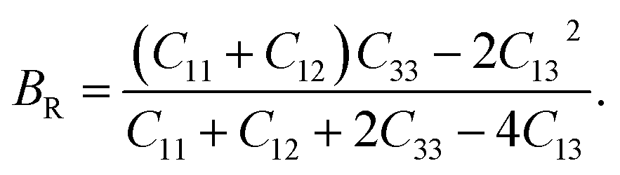
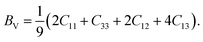
The elastic and shear moduli are expressed using Voigt and Reus approximation methods. The Voigt approximation82,83 is employed to calculate the bulk modulus of CTS crystals, which is given by the following equation:
| |
 | (15) |
The Reuss approximation84,85 represents the bulk modulus of CTS crystals by combining elastic constants:
| |
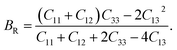 | (16) |
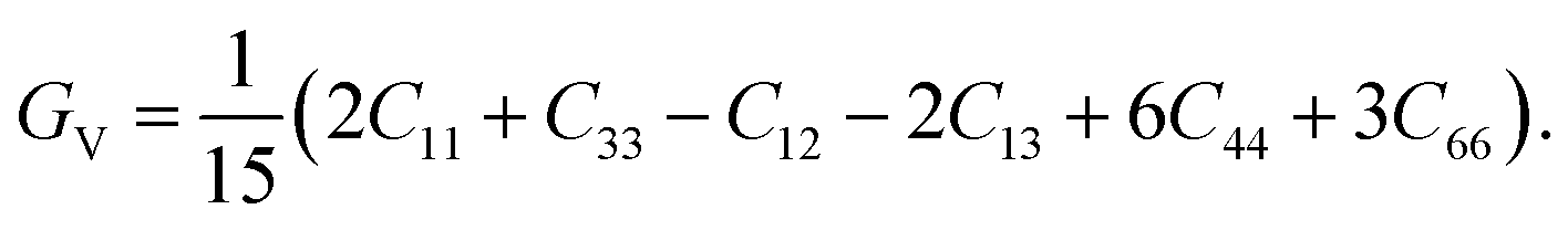
The Voigt of the shear modulus (Gv) of the CTS crystal is estimated as follows:86
| |
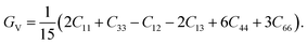 | (17) |
The Reuss shear modulus (GR) of the CTS crystal is approximated as follows:84
| | |
GR = 15{18BV/C2 + 6/(C11 − C12) + 6/C44 + 3/C66}−1.
| (18) |
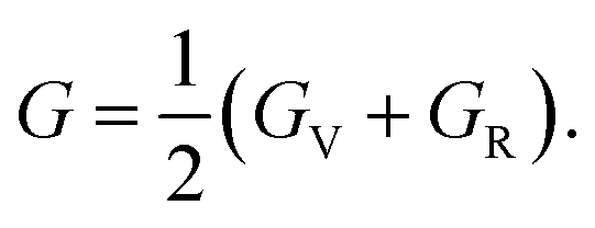
The bulk and shear moduli of the CTS crystals are calculated using Hill's approach,87 which suggests that the bulk (B) and shear (G) modulus are determined using an average value of the two approximation methods mentioned above.88 The values are calculated using the following equations:
| |
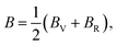 | (19) |
| |
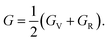 | (20) |
To calculate the Poisson's ratio, one utilizes B and G values:
| | |
σ = (3B − 2G)/(6B + 2G) = 0.320.
| (21) |
The Young's modulus of the CTS crystal is determined using B and G:
Table 4 shows determined bulk moduli BV, BR, B, shear moduli GV, GR, G (GPa), Young's moduli, Y (GPa), Poisson's ratio (n) and B/G ratio of CTS crystal at two different temperatures, 310 K and 953 K.
Table 4 Calculated bulk moduli (BV, BR, and an average of BV and BR (B)), shear moduli (GV, GR, and an average of GV and GR (G) (GPa)), Young's moduli (Y (GPa)), Poisson's ratio (n) and B/G ratio of CTS crystals at 310 K and 953 K
| Temperature (K) |
Bv |
BR |
B |
GV |
GR |
G |
B/G |
Y |
N |
| 310 |
47.69 |
58.65 |
53.17 |
14.62 |
20.20 |
17.41 |
3.26 |
39.80 |
0.36 |
| 953 |
32.71 |
54.24 |
43.48 |
16.11 |
21.52 |
18.82 |
2.02 |
41.53 |
0.28 |
The elastic constants estimated for CTS crystals at two different temperatures using the GGA approach within the DFT framework demonstrate that the crystals exhibit improved elastic stability at 953 K relative to room temperature (310 K).89,90 The estimated findings indicate a substantial anisotropy in CTS crystals, which is compatible with prior theoretical conclusions.81,91
6.3 Evaluation of the optical properties of CTS crystal
Optical properties of CTS crystals involve simulations of several parameters, such as dielectric function ε(ω), optical conductivity, reflectivity, refractive index (η) and energy loss function L(ω). As per the literature survey performed by the authors, the optical property simulations of CTS material are limited to tetragonal and triclinic phases only.25,49 Simulations based on the cubic CTS phase have not yet been reported.
6.3.1 Dielectric function. The linear optical properties of CTS crystals are evaluated using frequency-dependent Ehrenreich and Cohen's relation given by12| | |
ε(ω) = ε1(ω) + iε2(ω),
| (23) |
where ε1(ω) and iε2(ω) are the real and imaginary parts of the dielectric function, respectively. Fig. 8 shows a plot illustrating the real and imaginary dielectric functions of a CTS crystal that describes the optical characteristics of a CTS crystal. As in Fig. 8, the real component of the dielectric function ε1(ω) demonstrates an ascending trend with major peaks at 0.82 and 2.81 eV energies, succeeded by a subsequent decline and a negative trajectory spanning a broad energy spectrum. The modest Re(epsilon) signal at 2.81 eV energy is caused by a transition between the Cu(3d) and S(2p) states in the valence bands.
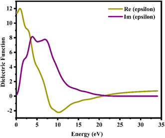 |
| | Fig. 8 Real and imaginary dielectric functions versus energy plots of the CTS crystal. | |
The imaginary component ε2(ω) of the dielectric function provides insights into how semiconductors interact with electromagnetic radiation during inter-band transitions, elucidating their absorptive behaviour within band structures.92 The peaks at 4.09 and 6.95 eV energies are due to an electronic transition involving the valence band of the Cu(3d) state and the conduction band of the Sn(3d) state, indicating a significant contribution to absorption behaviour. In Im(epsilon), the peak at 6.95 eV energy is caused by a transition within the Sn(3d) and S(2p) states. At low energies of 4.09 eV, an electrical transition occurs within the Cu(3d) and Sn(3d) states in the conduction band. The slight blue shifts in the major position energies are attributed to the localized degree of the S(2p) purity band. These studies reveal how multiple electrical states interact to shape the optical characteristics of CTS crystals.
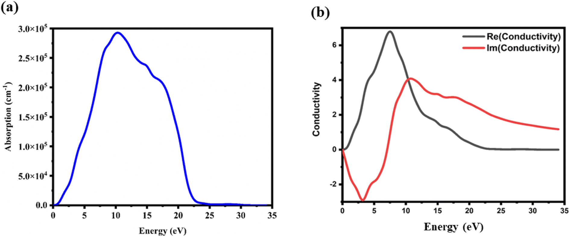
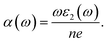
6.3.2 Optical conductivity and frequency-dependent absorption coefficient. Fig. 9(a) depicts the absorption coefficient curve of the CTS crystal computed using the following equation:12,66| |
 | (24) |
 |
| | Fig. 9 (a) Absorbance and (b) optical conductivity versus energy plots of the CTS crystal. | |
Notably, two absorption peaks (10.17 and 14.71 eV) are observed, signifying inter-band transitions involving the Cu(3d) state within the conduction band and the Sn(3p) and S(3p) levels within the valence band. These transitions exert a significant influence on the absorption behaviour of the CTS crystal. In the span of 2.5 eV to approximately 20 eV, the absorption coefficient peaks at 2.8 × 105 cm−1, followed by a decrease in photon energy and increases until reaching zero. These meticulous estimations provide invaluable details into the optical attributes of the CTS crystal, elucidating its behaviour across diverse photon energies and wavelengths.
The absorption characteristics of a crystal are intricately linked to its optical conductivity, denoted by σ(ω). Fig. 9(b) depicts a plot of the optical conductivity of the CTS crystal. As shown in Fig. 9(b), optical conductivity initiation is observed at specific frequencies; here, for (Re), it is at 7.41 eV and (Im) is at 10.73, 14.71, and 17.57 eV. These values demonstrate excellent optical response towards higher and lower energies. Photon energies below this threshold result in the suppression of the conductivity component, leading to complete cessation. Upon photon absorption, there is a notable enhancement in both the optical and electronic conductivity of the material, contributing to a substantial increase in conductivity in the CTS crystal.
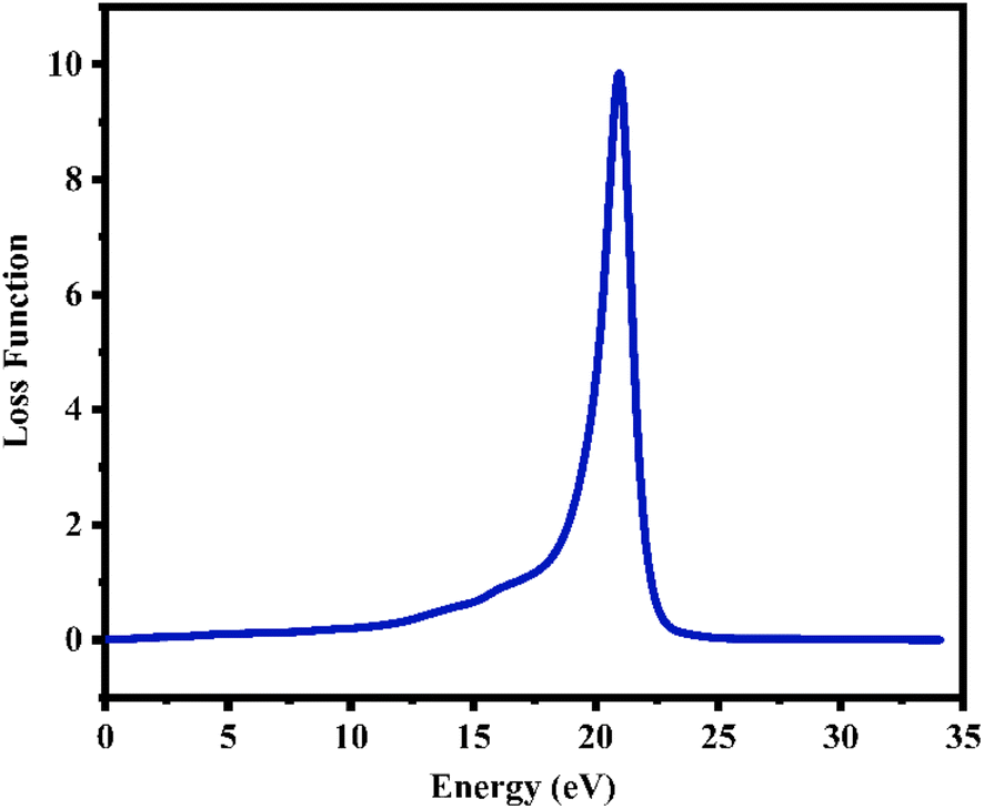
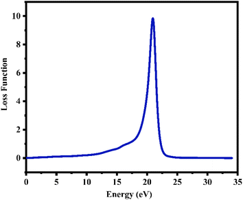
6.3.3 Loss function. The energy loss function L(ω) holds significant importance due to its capacity to forecast the propagation loss of energy within the material.93 Fig. 10 illustrates the estimated loss function for CTS crystal within the energy span of 15–18 eV. In the case of CTS crystals, the L(ω) spectrum exhibits a pronounced sharp peak, indicating energy loss occurring when the input photon energy surpasses the material's threshold. The peak observed at 20.92 eV relates to the trailing edges observed in the reflection spectrum.
 |
| | Fig. 10 Plot of loss function versus energy of the CTS crystal. | |
Notably, the peak in the loss function at 20.92 eV in the Cu–Sn–S system is due to intra-band transitions involving Cu(3d), Sn(3d), and S(3p) states within the conduction band. Particularly, the presence of the S(3p) state substantially contributes to the discernible peaks evident in the loss-function spectrum. The CTS crystal absorption spectrum depicted in Fig. 9(a) showcases a broad absorption zone, with a notable portion situated in the UV region. Within the Cu–Sn–S system, the transition among the Cu(3d), Sn(3d), and S(3p) states in the conduction band leads to heightened absorption below the absorption edge within the visible spectrum. Here, the dominance of the S(3p) state in the conduction band underscores absorption in the visible range.
6.3.4 Reflectivity and refractive index. The reflectivity R of a CTS crystal is determined by the following equation:12| |
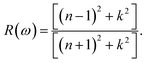 | (25) |
Here, n1 = 1 and n2 = n + ik. This formula considers the real (n) and imaginary (k) components of the refractive index, elucidating the interaction of light with the crystal. Fig. 11(a) illustrates the reflectivity spectrum of the CTS crystal with distinct peaks at 11.83, 15.14, and 18.83 eV. Evaluation of the spectrum reveals heightened reflectivity corresponding to higher energy levels. Energy peaks are mostly caused by transitions between Cu and Sn. The p and d states exhibit strong peaks, indicating their suitability as barriers to UV radiation. This distinctive pattern suggests the presence of robust conductivity within these specific energy ranges. The crystal's pronounced reflectivity facilitates efficient transmission and reflection of light in lower energy bands, underscoring its significant conductive characteristics.
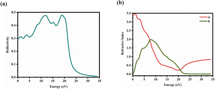 |
| | Fig. 11 (a) Reflectivity and (b) refractive index versus energy plot of the CTS crystal. | |
To ascertain the refractive index and extinction coefficient, the following formulas are utilized:94
The refractive index n(ω) is a crucial optical property used in industrial optical materials, such as photonic crystals, optical waveguides, solar cells, and detectors. This metric describes the quantity of light bent or refracted by semiconductor materials and tiny atomic interactions.45 Fig. 11(b) displays the static refractive index n(0). The figure depicts a peak in the refractive index occurring at approximately 0.93 and 3.02 eV. Furthermore, the extinction coefficient (k) exhibits peaks at 2.02, 4.12, and 7.92 eV, followed by a rapid decline beyond these points. These findings provide insights into the material's optical behaviour across different wavelengths, highlighting significant disparities in both refractive index and extinction coefficient along the electromagnetic spectrum. Table 5 shows the comparative analysis of the optical properties of CTS crystals compared to other forms and phases of CTS.
Table 5 Comparative analysis of optical properties of different forms and phases of the CTS crystal
| No. |
Material name |
Crystal structure |
Optical properties |
Ref. |
| 1 |
CTS TF (experimental) |
Tetragonal |
Transmittance and reflectance decrease below 1400 and 1250 nm, respectively; absorption coefficient: 5 × 104 cm−1; Eg: 1.34 eV |
43 |
| 2 |
CTS TF (experimental) |
Monoclinic, tetragonal, monoclinic |
Structural dependent optical properties; absorption coefficient: 2.3 × 104 cm−1; Eg: 1.18–1.37 eV |
95 |
| 3 |
CTS NPs (experimental) |
Cubic, tetragonal, monoclinic |
Solvent-dependent optical study; change in bandgap is observed in the case of water (1.60 eV), ethylene glycol (1.43 eV) and EW (1.48 eV) |
18 |
| 4 |
CTS NPs (theoretical) |
— |
Doping and effect on bandgap using z-scan method; absorption coefficient: 10−16 W cm−2; refractive index: 10−20 W cm−1; 3rd order susceptibility: 10−13 esu ratio |
96 |
| 5 |
CTS compound (theoretical) |
— |
DFT framework; absorption coefficient: 105 cm−1; reflectance: 2.3%; refractive index: 2.90, electron energy loss: 19 eV |
97 |
| 6 |
CTS TF (experimental) |
Triclinic |
Average optical transmission: 10–30%; less reflection of 20 and above absorption edge; absorption coefficient: > 104 cm−1; Eg: 2.34 to 1.49 eV; refractive index: 3.37–1.93; extinction coefficient: 0.07 to 0.19; εr: 4 to 11; εi: 0.3 to 1.4; optical conductivity: ∼1012 S−1 |
98 |
| 7 |
CTS TF (experimental + theoretical) |
Tetragonal, monoclinic, tetragonal |
Transmittance decreases between 700–1400 nm; absorption coefficient: 1.5 × 104 cm−1; Eg: 1.1 and 1.5 eV |
99 |
| 8 |
CTS crystal (experimental + theoretical) |
Cubic |
Absorption coefficient: 2.8 × 105 cm−1; refractive index: 0.93 and 3.02 eV; extinction coefficient: 2.018, 4.12, and 7.92 eV; energy loss function: 20.92 eV; optical conductivity for (Re) has peak at 7.41 eV and (Im) at 10.73, 14.71, and 17.57 eV; real component of the dielectric function ε1(ω) has peaks at 0.82 and 2.81 eV and imaginary component ε2(ω) at 4.09 and 6.95 eV |
Present work |
6.4 Evaluation of band structure and density of states of CTS crystals
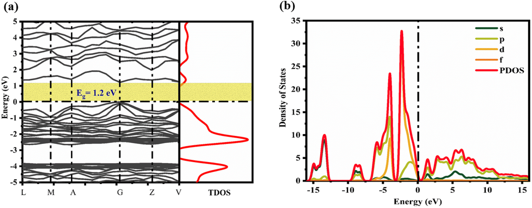
The electronic band structure of CTS crystals and density of states (DOS) at ambient temperature and pressure are determined using the PBE + GGA screened function demonstrated in Fig. 12(a and b). The total and projected valence band densities of TDOS and PDOS states, respectively, are employed to evaluate the band structure and DOS of the CTS crystal. Fig. 12(a) shows the highest and lowest points of the valence and conduction bands of the CTS crystals, respectively.
 |
| | Fig. 12 (a) Electronic band structure and (b) DOS of CTS crystals. | |
The computational results show that the CTS crystal has a bandgap of 1.2 eV. The result well matches the experimental band gap value obtained by DRS, which is obtained as 1.23 eV. The match states systematic accuracy in the GGA theory. This work employed the scissor factor to rectify the huge energy gap mistake in LDA calculations.89,99 The electron density is illustrated in Fig. 12(b), showing that the bandgap around the Fermi surface is mostly influenced by p- and d-state electrons, with minor contributions from s-state electrons. The valence band maximum at −2.5 eV is primarily made up of the 3d state of Cu and the 3p state of S in the electron density. The conduction band energy levels above the Fermi surface include the 3p state of Cu, 4p state of Sn, and 3p state of S.
As shown in Fig. 12(b), the valence band comprises Cu-3d orbitals, with a slight contribution from S-3p orbitals. The conduction band largely consists of S-3p orbitals, with little contribution from Sn-5s orbitals.56 The lowest valence band (−10 to −7.5 eV) is primarily made up of occupied Sn-5s and S-3p states, while the highest valence band (−7.5 to 0 eV) is primarily made up of occupied Cu-3d and S-3p states, and the conduction the band (0 to 15 eV) is mostly made up of unoccupied Sn-5s and S-3p states. The form and peak locations of PDOS associated with Cu, Sn, and S atoms are consistent with previous observations.99 The electronic states of Cu, Sn, and S atoms in CTS crystal are comparable to those observed in other quaternary Cu, Sn and S-based compounds, such as Cu2HgSnS4.100
7. Conclusion
The crystals of CTS are grown using the DVT technique. The XRD analysis confirmed that the as-grown crystals possessed a cubic unit cell structure with a lattice parameter of 5.403 Å. The XPS survey spectrum of the as-grown CTS crystals revealed discernible peaks related to the presence of Cu, Sn and S along with minor oxygen content. The DRS analysis of the CTS crystals depicted an absorption edge of around 632.44 nm, signifying visible range absorption by as-grown CTS crystals. Tauc plot using the Kubelka–Munk function demonstrated a direct bandgap of 1.23 eV of as-grown CTS crystals. The thermal investigation of the as-grown CTS crystals utilizing TG, DTG, and DTA curves revealed four steps of decomposition. A comparative analysis of the elastic properties revealed a significant increase in the elasticity of the CTS crystal when exposed to an elevated temperature of 953 K compared to room temperature (310 K). In dielectric properties, the observed peaks in the ε1(ω) plot at 0.82 and 2.81 eV energies showed the CTS crystal's efficiency in storing electrical energy at specific frequencies. The observed peak in Re(epsilon) at 2.81 eV energy is due to valence band transitions between the Cu(3d) and S(2p) states. Optically, the CTS crystal exhibits a pronounced absorption coefficient peak of 2.8 × 105 cm−1, followed by a decreasing trend with photon energy increase until it reaches zero. The optical conductivity actuation is observed in (Re) at 7.41 eV and (Im) at 10.73, 14.71, and 17.57 eV. The theoretically estimated bandgap of 1.2 eV matches well with the observed optical conductivity and absorption characteristics of the CTS crystal, fortifying the theoretical estimation of its electronic structure. In the loss function, the peak observed at 20.92 eV in the CTS crystal is due to intra-band transitions of the Cu(3d), Sn(3d), and S(3p) states, demonstrating significant electron dynamics within the conduction of the band. As far as the refractive index of the CTS crystal is concerned, peaks are observed at 0.93 and 3.02 eV. The extinction coefficient k exhibits peaks at 2.02, 4.12, and 7.92 eV, with a rapid decrease after these points. The electronic band structure of the CTS crystal reveals that the valence band maximum is composed of contributions from the Cu(3d) and S(3p) states. The conduction the band energy levels include the 3p state of Cu, the 4p state of Sn, and the 3p state of S. The evaluation of the structural properties of CTS crystal showed that the bond length for all Cu–S bonds is 2.33 Å, depicting a uniform bond structure. For the Sn–S bonds, the measurement showed three shorter bonds of 2.60 Å and three longer bonds of 2.67 Å for these elements, demonstrating a well-defined coordination environment around the tin atoms. Precise tuning and modifications of theoretical parameters of optical and electrical properties of CTS crystal make it a potential material for an extensive range of applications, such as in photovoltaics, UV-visible-IR photodetectors, display devices, and light emitting diodes. Additionally, it provides a comprehensive overview of how the CTS crystal behaves under varying light conditions. Tuning and modifications of the elastic properties of CTS crystals have practical applications in various automotive industries, such as shock absorbers, suspension systems, and vibration dampers, as well as in the packaging industry, such as elastic bands and cushioning materials. Modifications on band structure and structural properties of CTS provide several chances to improve the CTS crystal's overall response to various thermal and electrical transport properties.
Data availability
The data included in this manuscript is completely carried out by the authors.
Conflicts of interest
There is no conflict of interest to declare for this work.
Acknowledgements
The authors of this manuscript are thankful to Dr Jayesh Gandhi for XRD, Sophisticated Instrumentation Centre for Applied Research and Testing (SICART) for DRS and Sprint Testing Solutions for XPS.
References
- M. Pumera, Z. Sofer and A. Ambrosi, J. Mater. Chem. A, 2014, 2, 8981–8987 RSC.
- H. D. Shelke, A. R. Machale, A. A. Survase, H. M. Pathan, C. D. Lokhande, A. C. Lokhande, S. F. Shaikh, A. ul, H. S. Rana and M. Palaniswami, Materials, 2022, 15, 3126 CrossRef CAS PubMed.
- F. Bozheyev, J. Mater. Chem. A, 2023, 11, 19845–19853 RSC.
- A. Paul, B. Krishnan, S. Shaji and D. A. Avellaneda, Appl. Surf. Sci., 2023, 639, 158181 CrossRef CAS.
- G. Konstantatos, J. Clifford, L. Levina and E. H. Sargent, Nat. Photonics, 2007, 1, 531–534 CrossRef CAS.
- S. R. Patel, S. H. Chaki, R. K. Giri, A. J. Khimani, Y. H. Vaidya, P. Thakor, A. B. Thakkar and M. P. Deshpande, ACS Appl. Bio Mater., 2023, 2211–2225 CrossRef CAS PubMed.
- R. K. Giri, S. Chaki, A. J. Khimani, Y. H. Vaidya, P. Thakor, A. B. Thakkar, S. J. Pandya and M. P. Deshpande, ACS Omega, 2021, 6, 26533–26544 CrossRef CAS PubMed.
- P. Goswami and G. Gupta, Mater. Today Chem., 2022, 23, 100726 CrossRef CAS.
- K. Lohani, H. Nautiyal, N. Ataollahi, C. Fanciulli, I. Sergueev, M. Etter and P. Scardi, J. Phys. Chem. C, 2020, 125, 178–188 CrossRef.
- F. Gygi, J. Chem. Theory Comput., 2023, 19, 1300–1309 CrossRef CAS PubMed.
- A. Grisafi, A. M. Lewis, M. Rossi and M. Ceriotti, J. Chem. Theory Comput., 2022, 19, 4451–4460 CrossRef PubMed.
- R. K. Giri, S. H. Chaki, M. S. Dave, S. R. Bharucha, A. J. Khimani, R. M. Kannaujiya, M. P. Deshpande and M. B. Solanki, Mater. Adv., 2023, 4, 3246–3256 RSC.
- A. S. Kshirsagar, P. V More and P. K. Khanna, RSC Adv., 2016, 6, 86137–86150 RSC.
- W. Wang, G. Zhi, L. Liu, L. Cao, J. Xie, L. Sun, L. Hao and H. Yao, J. Nanoparticle Res., 2022, 24, 1–10 CrossRef.
- H.-I. Hsiang, C.-T. Yang and J.-H. Tu, RSC Adv., 2016, 6, 99297–99305 RSC.
- B. Kumar, S. V. Singh, A. Chattopadhyay, S. Biring and B. N. Pal, ACS Omega, 2020, 5, 25947–25953 CrossRef CAS PubMed.
- J. Lu, J. Yang, D. Yang, S. Hu, Q. Sun, G. Yang, S. Gai, Z. Wang and P. Yang, J. Mater. Chem. B, 2021, 9, 336–348 RSC.
- K. M, H. Shamima, G. R and V. K, Mater. Technol., 2018, 33, 72–78 CrossRef.
- T. Bayazıt, M. A. Olgar, T. Küçükömeroğlu, E. Bacaksız and M. Tomakin, J. Mater. Sci. Mater. Electron., 2019, 30, 12612–12618 CrossRef.
- A. Haque, S. Ershadrad, T. D. Chonamada, D. Saha, B. Sanyal and P. K. Santra, J. Mater. Chem. A, 2022, 10, 19925–19934 RSC.
- M. Liu, C.-Y. Lai, C.-Y. Chang and D. R. Radu, Crystals, 2021, 11(1), 51 CrossRef CAS.
- S. Thiruvenkadam, P. Sakthi, S. Prabhakaran, S. Chakravarty, V. Ganesan and A. L. Rajesh, Phys. B Condens. Matter, 2018, 538, 8–12 CrossRef CAS.
- M. S. Abdel-Latif, A. Rezk, N. M. Shaalan, A. Abdel-Moniem and A. Hessein, J. Nanoparticle Res., 2021, 23, 216 CrossRef CAS.
- Y. Shen, C. Li, R. Huang, R. Tian, Y. Ye, L. Pan, K. Koumoto, R. Zhang, C. Wan and Y. Wang, Sci. Rep., 2016, 6, 32501 CrossRef CAS PubMed.
- S. B. Jathar, S. R. Rondiya, Y. A. Jadhav, D. S. Nilegave, R. W. Cross, S. V Barma, M. P. Nasane, S. A. Gaware, B. R. Bade, S. R. Jadkar, A. M. Funde and N. Y. Dzade, Chem. Mater., 2021, 33, 1983–1993 CrossRef CAS PubMed.
- D. Tiwari, T. K. Chaudhuri, T. Shripathi and U. Deshpande, J. Phys. Chem. Solids, 2014, 75, 410–415 CrossRef CAS.
- F. Oliva, L. Arqués, L. Acebo, M. Guc, Y. Sánchez, X. Alcobé, A. Pérez-Rodríguez, E. Saucedo and V. Izquierdo-Roca, J. Mater. Chem. A, 2017, 5, 23863–23871 RSC.
- L. Shi, W. Wang, C. Wu, J. Ding and Q. Li, J. Alloys Compd., 2017, 699, 517–520 CrossRef CAS.
- A. R. Machale, S. A. Phaltane, H. D. Shelke and L. D. Kadam, Mater. Today Proc., 2021, 43, 2768–2773 CrossRef CAS.
- X. He, Z. Ling, X. Peng, X. Yang, L. Ma and S. Lu, Electrochem. Commun., 2023, 148, 107441 CrossRef CAS.
- A. C. Lokhande, S. A. Pawar, E. Jo, M. He, A. Shelke, C. D. Lokhande and J. H. Kim, Opt. Mater., 2016, 58, 268–278 CrossRef CAS.
- M. Hegedüs, M. Baláž, M. Tešinský, M. J. Sayagués, P. Siffalovic, M. Kruľaková, M. Kaňuchová, J. Briančin, M. Fabián and P. Baláž, J. Alloys Compd., 2018, 768, 1006–1015 CrossRef.
- S. P. Meenakshisundaram and M. B. Sridharan, J. Alloys Compd., 2024, 981, 173734 CrossRef CAS.
- V. Maheskumar, P. Gnanaprakasam, T. Selvaraju and B. Vidhya, Int. J. Hydrogen Energy, 2018, 43, 3967–3975 CrossRef CAS.
- A. C. Lokhande, A. Shelke, P. T. Babar, J. Kim, D. J. Lee, I.-C. Kim, C. D. Lokhande and J. H. Kim, RSC Adv., 2017, 7, 33737–33744 RSC.
- Z. Yu, W. Li, N. Cheng, Z. Liu, B. Lei, Z. Xiao, W. Zi, Z. Zhao and Y. Tu, ACS Appl. Nano Mater., 2022, 5, 10755–10762 CrossRef CAS.
- P. Zhao and S. Cheng, Adv. Mater. Sci. Eng., 2013 DOI:10.1155/2013/726080.
- M. H. Sayed, E. V. C. Robert, P. J. Dale and L. Gütay, Thin Solid Films, 2019, 669, 436–439 CrossRef CAS.
- T. A. Kuku and O. A. Fakolujo, Sol. Energy Mater., 1987, 16, 199–204 CrossRef CAS.
- S. A. Vanalakar, G. L. Agawane, A. S. Kamble, C. W. Hong, P. S. Patil and J. H. Kim, Sol. Energy Mater. Sol. Cells, 2015, 138, 1–8 CrossRef CAS.
- B. Patel, R. Narasimman, R. K. Pati, I. Mukhopadhyay and A. Ray, in AIP Conference Proceedings, AIP Publishing LLC, 2018, vol. 1961, p. 30046 Search PubMed.
- H. D. Shelke, A. C. Lokhande, J. H. Kim and C. D. Lokhande, J. Colloid Interface Sci., 2017, 506, 144–153 CrossRef CAS PubMed.
- H. Dahman, S. Rabaoui, A. Alyamani and L. El Mir, Vacuum, 2014, 101, 208–211 CrossRef CAS.
- Y. Igarashi, T. Tomono, K. Tanaka and K. Moriya, Jpn. J. Appl. Phys, 2022, 61, SB1002 CrossRef CAS.
- J. Raval, B. Shah, D. Kumar, S. H. Chaki and M. P. Deshpande, Chem. Eng. Sci., 2024, 119728 CrossRef CAS.
- M. P. Suryawanshi, U. V Ghorpade, S. W. Shin, S. A. Pawar, I. Y. Kim, C. W. Hong, M. Wu, P. S. Patil, A. V Moholkar and J. H. Kim, ACS Appl. Mater. Interfaces, 2016, 8, 11603–11614 CrossRef CAS PubMed.
- S. Dias and S. B. Krupanidhi, AIP Adv., 2016, 6, 25217 CrossRef.
- A. C. Lokhande, A. A. Yadav, J. Lee, M. He, S. J. Patil, V. C. Lokhande, C. D. Lokhande and J. H. Kim, J. Alloys Compd., 2017, 709, 92–103 CrossRef CAS.
- R. Dahule, A. Raghav, A. T. Hanindriyo, K. Hongo, R. Maezono and E. Panda, Adv. Theory Simul., 2021, 4, 2000315 CrossRef CAS.
- Y. Matsumoto, N. Aihara, A. Munemura and K. Tanaka, Mater. Lett., 2016, 170, 213–216 CrossRef CAS.
- J. B. Raval, S. H. Chaki, B. S. Shah and M. P. Deshpande, Mater. Today Proc., 2023, 73(Part 4), 562–566 CrossRef CAS.
- Y. Kim and I.-H. Choi, J. Alloys Compd., 2019, 770, 959–963 CrossRef CAS.
- P. Giannozzi, J. Phys.: Condens. Matter, 2009, 21, 39 CrossRef PubMed.
- C. Wang, X. Li and Y. Wang, in 7th International Conference on Management, Education, Information and Control (MEICI 2017), Atlantis Press, 2017, pp. 176–180 Search PubMed.
- J. P. Perdew, K. Burke and M. Ernzerhof, Phys. Rev. Lett., 1996, 77, 3865 CrossRef CAS PubMed.
- T. ALWAN and M. JABBAR, Turk. J. Phys., 2010, 34, 107–116 CAS.
- J. Grechenkov, A. Gopejenko, D. Bocharov, I. Isakoviča, A. I. Popov, M. G. Brik and S. Piskunov, Energies, 2023, 16, 4823 CrossRef CAS.
- D. R. Hamann, Phys. Rev. B, 2013, 88, 85117 CrossRef.
- D. J. Singh and L. Nordstrom, Planewaves, Pseudopotentials, and the LAPW Method, Springer Science & Business Media, 2006 Search PubMed.
- G. B. Bachelet, D. R. Hamann and M. Schlüter, Phys. Rev. B, 1982, 26, 4199 CrossRef CAS.
- P. K. Lam, M. L. Cohen and A. Zunger, Phys. Rev. B, 1980, 22, 1698 CrossRef CAS.
- G. Florio, Structural Features of Magnetic Materials, Encyclopedia of Smart Materials, ed. A.-G. Olabi, Elsevier, 2022, vol. 5, pp. 1–9 Search PubMed.
- S. FANa and Z. LUb, Therm. Sci., 2022, 26, 2823–2830 CrossRef.
- M. B. Solanki, S. Shinde and B. B. Parekh, Mater. Today Proc., 2022, 67, 943–947 CrossRef CAS.
- M. B. Solanki, P. Patel, S. Shinde, B. B. Parekh and M. Joshi, Ferroelectrics, 2021, 571, 1–25 CrossRef CAS.
- M. B. Solanki, M. Jani, S. M. Vyas, B. B. Parekh, A. D. Oza, C. Prakash and B. Singh, Proc. Inst. Mech. Eng. Part E J. Process Mech. Eng., 2023, 09544089231206124 CrossRef.
- M. Belaqziz, K. Medjnoun, K. Djessas, H. Chehouani and S. E. Grillo, Mater. Res. Bull., 2018, 99, 182–188 CrossRef CAS.
- B. D. Cullity, Elements of X-ray Diffraction, Addison-Wesley, 2nd edn, 1979 Search PubMed.
- M. Vincent, V. Sai Avvaru, M. Haranczyk and V. Etacheri, Chem. Eng. J., 2022, 433, 133810 CrossRef CAS.
- A. Roy, A. K. Mukhopadhyay, S. C. Das, G. Bhattacharjee, A. Majumdar and R. Hippler, Coatings, 2019, 9, 551 CrossRef CAS.
- H. D. Shelke, A. C. Lokhande, A. M. Patil, J. H. Kim and C. D. Lokhande, Surface. Interfac., 2017, 9, 238–244 CrossRef CAS.
- R. K. Giri, S. H. Chaki, A. J. Khimani, S. R. Patel and M. P. Deshpande, Eur. Phys. J. Plus, 2021, 136, 320 CrossRef CAS.
- S. Patel, S. H. Chaki and P. C. Vinodkumar, Thermochim. Acta, 2020, 689, 178614 CrossRef CAS.
- P. R. Guddeti, S. Gedi and K. T. R. Reddy, Mater. Sci. Semicond. Process., 2018, 86, 164–172 CrossRef CAS.
- V. Nurliyanti, B. Pranoto, Y. Gunawan and B. Munir, in AIP Conference Proceedings, AIP Publishing, 2024, vol. 3003 Search PubMed.
- C.-P. T. Nguyen, P. Schoenherr, L. Juli and J. Seidel, Nanoscale, 2021, 13, 16959–16967 RSC.
- S.-J. Wu, P.-C. Chin and H. Liu, Appl. Sci., 2019, 9, 2067 CrossRef CAS.
- M. Born and K. Huang, Dynamical Theory of Crystal Lattices, Oxford university press, 1996 Search PubMed.
- M. Jamal, S. Jalali Asadabadi, I. Ahmad and H. A. Rahnamaye Aliabad, Comput. Mater. Sci., 2014, 95, 592–599 CrossRef CAS.
- B. B. Karki, G. J. Ackland and J. Crain, J. Phys. Condens. Matter, 1997, 9, 8579 CrossRef CAS.
- F. Birch, Phys. Rev., 1947, 71, 809 CrossRef CAS.
- H. Eisenschmidt, A. Voigt and K. Sundmacher, Cryst. Growth Des., 2015, 15, 219–227 CrossRef CAS.
- F. Machui, L. Lucera, G. D. Spyropoulos, J. Cordero, A. S. Ali, P. Kubis, T. Ameri, M. M. Voigt and C. J. Brabec, Sol. Energy Mater. Sol. Cell., 2014, 128, 441–446 CrossRef CAS.
- J. F. Kielkopf, J. Opt. Soc. Am., 1973, 63, 987–995 CrossRef.
- I. R. Shein and A. L. Ivanovskii, J. Phys. Condens. Matter, 2008, 20, 415218 CrossRef.
- T. Ida, M. Ando and H. Toraya, J. Appl. Crystallogr., 2000, 33, 1311–1316 CrossRef CAS.
- Y. Liu, J. Lin, G. Huang, Y. Guo and C. Duan, J. Opt. Soc. Am. B, 2001, 18, 666–672 CrossRef CAS.
- D. H. Chung and W. R. Buessem, J. Appl. Phys., 1967, 38, 2535–2540 CrossRef CAS.
- S. M. Ahmad, Appl. Phys. A, 2017, 123, 1–9 CrossRef.
- J. Radhakrishnan, A. Kareem, S. Ratna, S. Senthilkumar and K. Biswas, ACS Omega, 2022, 7, 43883–43893 CrossRef CAS PubMed.
- S. I. Ranganathan and M. Ostoja-Starzewski, Phys. Rev. Lett., 2008, 101, 55504 CrossRef PubMed.
- B. Y. Taher and A. S. Ahmed, Chalcogenide Lett., 2021, 18, 717–724 CrossRef CAS.
- Z. Li, J. M. Gong, Y. Harada, B. Da, R. G. Zeng and Z. J. Ding, Results Phys., 2024, 56, 107247 CrossRef.
- W. Tang, S. S. Rassay and N. M. Ravindra, Madridge J. Nanotechnol. Nanosci, 2017, 2, 58–64 CrossRef.
- M. Y. Zaki, F. Sava, I. D. Simandan, A. T. Buruiana, C. Mihai, A. Velea and A. C. Galca, Sci. Rep., 2022, 12, 7958 CrossRef CAS PubMed.
- Y. Gündoğdu, A. HouimI, S. Y. Gezgin and H. Ş. Kiliç, Plasmonics, 2024 DOI:10.1007/s11468-023-02189-x.
- A. O. Isyaku, Structural, Electronic and Optical Properties of Cu 2 Sns 3 Solar Absorber: A First-Principle Density Functional Theory Investigation, Masters thesis, African University of Science and Technology, 2019.
- P. R. Guddeti, P. M. B. Devi and K. T. R. Reddy, Chin. J. Phys., 2020, 67, 458–472 CrossRef CAS.
- N. Thota, M. Kumar, M. Vishwakarma and B. R. Mehta, Thin Solid Films, 2019, 677, 62–67 CrossRef CAS.
- T. V Vu, A. A. Lavrentyev, B. V Gabrelian, H. D. Tong, V. A. Tkach, O. V Parasyuk and O. Y. Khyzhun, Opt. Mater., 2019, 96, 109296 CrossRef.
|
| This journal is © The Royal Society of Chemistry 2024 |
Click here to see how this site uses Cookies. View our privacy policy here. 
 Open Access Article
 This Open Access Article is licensed under a Creative Commons Attribution-Non Commercial 3.0 Unported Licence
 *a,
Sunil H. Chaki*a,
Sefali R. Patel
*a,
Sunil H. Chaki*a,
Sefali R. Patel