DOI:
10.1039/D4RA04107K
(Paper)
RSC Adv., 2024,
14, 21982-21990
A first-principles prediction of novel Janus ZrGeZ3H (Z = N, P, and As) monolayers: Raman active modes, piezoelectric responses, electronic properties, and carrier mobility
Received
5th June 2024
, Accepted 6th July 2024
First published on 11th July 2024
Abstract
In this article, an attempt is made to explore new materials for applications in piezoelectric and electronic devices. Based on density functional theory calculation, we construct three Janus ZrGeZ3H (Z = N, P, and As) monolayers and study their stability, piezoelectricity, Raman response, and carrier mobility. The results from phonon dispersion spectra, ab initio molecular dynamics simulation, and elastic coefficients confirm the structural, thermal, and mechanical stability of these proposed structures. The ZrGeZ3H monolayers are indirect band gap semiconductors with favourable band gap energy of 1.15 and 1.00 eV for the ZrGeP3H and ZrGeAs3H, respectively, from Heyd–Scuseria–Ernzerhof functional method. It is found that the Janus ZrGeZ3H monolayers possess both in-plane and out-of-plane piezoelectric coefficients, revealing that they are potential piezoelectric candidates. In addition, the carrier mobilities of electrons and holes along transport directions are anisotropic. Notably, the ZrGeP3H and ZrGeAs3H monolayers have high electron mobility of 3639.20 and 3408.37 cm2 V−1 s−1, respectively. Our findings suggest the potential application of the Janus ZrGeZ3H monolayers in the piezoelectric and electronic fields.
1 Introduction
It is well known that fossil fuels such as oil and coal are non-renewable energy sources. In addition, using these fossil fuels induces high emissions of CO2 and other pollutants resulting in severe problems of global warming and environmental pollution. Therefore, many efforts have been made to find new alternative energy sources. Piezoelectric technology is an attractive approach for renewable and environmentally friendly energies. Based on the piezoelectric effect, piezoelectric materials can generate electricity from mechanical energy or vice versa. The piezoelectric properties of materials are closely related to the symmetry of crystal structure.1–3 A piezoelectric material needs to have a non-centrosymmetric structure. Thus, studies on materials that have non-centrosymmetric structures for piezoelectric response are necessary.
The Janus two-dimensional (2D) materials have been explored with various unique features such as electronic,4,5 optical,6 catalytic,7,8 thermoelectric,9 piezoelectric,10,11 properties due to their intrinsic asymmetry structures.12,13 Especially, experimental and theoretical works have demonstrated the application prospects of 2D materials in the piezoelectric field. For instance, Duerloo et al. discovered the intrinsic piezoelectricity in 2D transition metal dichalcogenides based on the density functional theory investigations. The high in-plane piezoelectric coefficients of 9.13 pm V−1 were obtained for MoTe2 material.14 The GaSe and SnSe monolayers were also revealed to be piezoelectric materials with high piezoelectric coefficients.15,16 Interestingly, the Janus structures with the broken mirror symmetry caused out-of-plane polarization dipole, resulting in an additional out-of-plane piezoelectricity. Guo and co-workers constructed Janus structures of group III monochalcogenides by first-principles calculations. They found that these group III Janus chalcogenides exhibited piezoelectricity with both in-plane piezoelectric coefficients (up to 8.47 pm V−1) and extra out-of-plane piezoelectric coefficient of 0.07–0.46 pm V−1.17 Some other 2D Janus structures also possessed additional out-of-plane piezoelectric effect such as XTeI (X = Sb/Bi),18 MoSTe,19 MoSO,20 γ-Sn2XY (X and Y are the chalcogen atoms),21 and BMX2 (M = Ga or In; X = S/Se).22
The recent experimental discovery of 2D MoSi2N4 and WSi2N4 monolayers has promoted great interest in 2D materials which composed from seven atoms.23 Consequently, a family of 2D materials with the general formula MA2Z4 has been theoretically reported.24 The MA2Z4 family exhibits high structural stability and outstanding physical properties. Some Janus materials have been derived from the MA2Z4 family, such as MSiGeN4,25 MGeSiP4,26 and XMoSiN2.27 These Janus compounds also exhibit piezoelectric properties, making them suitable for applications in piezoelectric devices.
Inspired by the need for new materials for renewable energy and the research on Janus MA2N4-based materials, in this article, we design 2D Janus ZrGeZ3H (Z = N, P, and As) monolayers, and predict their stabilities, structural and electronic characteristics, Raman response, and carrier mobility by using the first-principles calculations. At the same time, we also investigate the piezoelectric properties in these monolayers.
2 Computational details
Based on density functional theory (DFT), to investigate the electronic structures of material we used the projector augmented wave method as implemented in the Vienna ab initio simulation package (VASP).28,29 We employed the GGA parameterized by Perdew, Burke, and Ernzerhof (PBE) to study the exchange–correlation potential.30 To gain more accurate results for band structure, we used the hybrid functional suggested by Heyd, Scuseria and Ernzerhof (HSE06).31 The phonon calculations were performed by the VASP+PHONOPY code using the density functional perturbation theory (DFPT).32 We set the convergence threshold for force and energy as 10−3 eV Å−1 and 10−6 eV, respectively. We selected a 12 × 12 × 1 k-point grid to sample the first Brillouin zone (BZ). The energy cut-off for a plane wave basis was 650 eV. We set up a 20 Å vacuum to eliminate interlayer interactions. The interactions of van der Waals (vdW) between the layers were described by the semi-empirical DFT-D3 method.33 The Raman activity was tested by calculating the macroscopic dielectric tensor.34 Within DFPT, we computed the elastic tensors and piezoelectric stress tensors. Ab initio molecular dynamics (AIMD) calculation was used35 to test the thermodynamic stability of Janus systems. We corrected our computation with the dipole adjustment to correct for the dipole moment inherent in the asymmetric material. The carrier mobility in the materials was computed using the deformation potential approach.36
3 Results and discussion
3.1 Structure, stability, and Raman activity
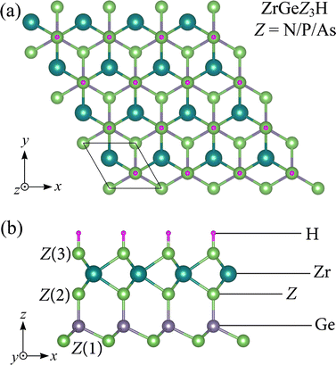
Fig. 1 illustrates the crystal structure with the unit cell of Janus ZrGeZ3H monolayers in equilibrium. The 2D ZrGeZ3H crystal structures are built from the ZrGe2Z4 symmetric monolayers by simultaneously removing the GeZ atomic layer and replacing it with an H atomic layer. The 2D Janus ZrGeZ3H monolayers have a vertically asymmetric structure concerning the central atomic layer Zr. The unit cell of ZrGeZ3H contains six atoms as shown in Fig. 1. We calculate the structural parameters of the Janus ZrGeZ3H monolayers and list them in Table 1. The results show that the values of lattice constant, bond length as well as thickness of the monolayer gradually increase with the increasing atomic number of Z element. The ZrGeN3H, ZrGeP3H, and ZrGeAs3H monolayers have lattice constant (a) of 3.18, 3.76, and 3.90 Å, respectively. These achieved values are comparable to those of the reported ZrGe2Z4 monolayer.24
 |
| | Fig. 1 (a) Top and (b) side views of the ZrGeZ3H (Z = N, P, and As) crystal structures. | |
Table 1 Lattice constant a (Å), thickness h (Å) bond length d (Å), and cohesive energy Ecoh (eV per atom) of Janus ZrGeZ3H monolayers
| |
a |
h |
d1 |
d2 |
d3 |
d4 |
d5 |
Ecoh |
| ZrGeN3H |
3.18 |
5.90 |
2.20 |
2.21 |
1.88 |
1.92 |
1.03 |
−7.23 |
| ZrGeP3H |
3.76 |
7.68 |
2.63 |
2.61 |
2.31 |
2.39 |
1.42 |
−5.52 |
| ZrGeAs3H |
3.90 |
8.08 |
2.72 |
2.71 |
2.41 |
2.50 |
1.53 |
−5.08 |
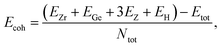
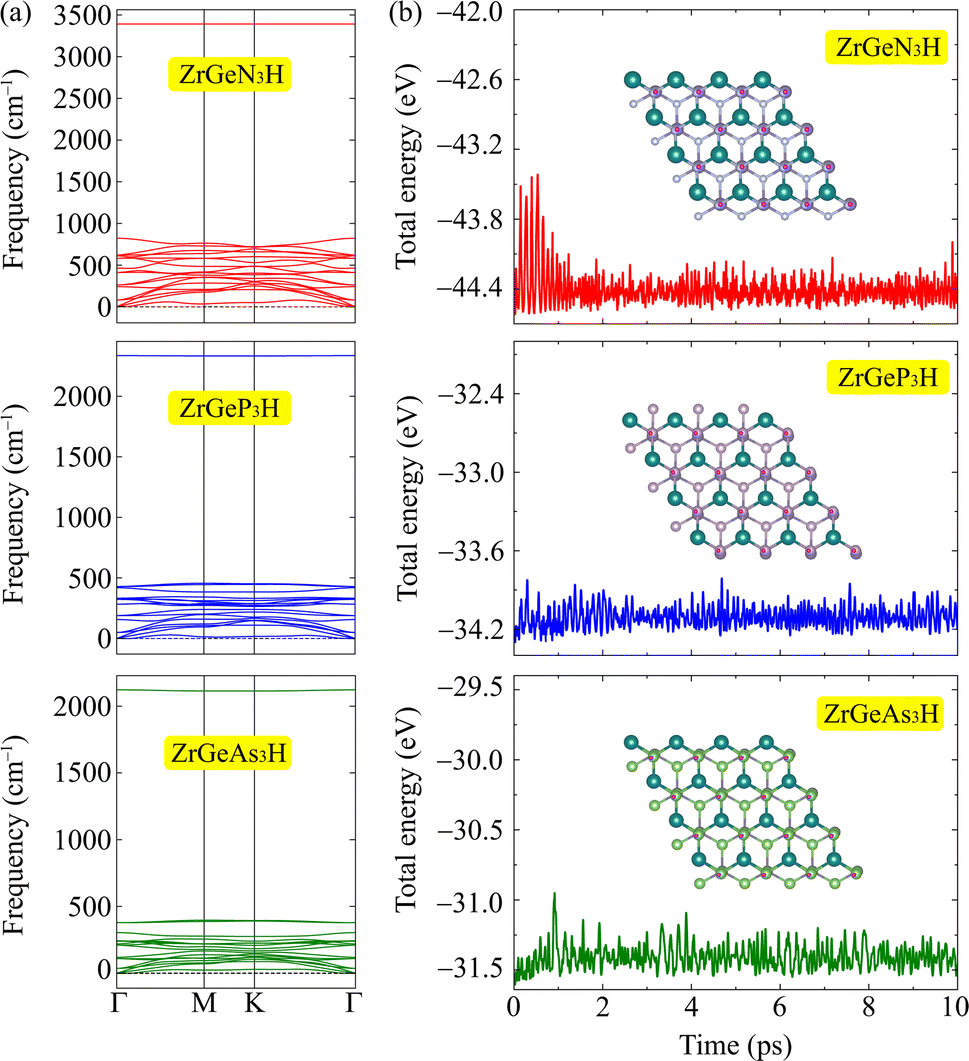
After calculating the structural parameters of the 2D ZrGeZ3H crystals, we examine their structural stability to explore their feasibility under conventional conditions. Fig. 2 depicts phonon dispersion spectra and AIMD simulations of all three Janus ZrGeZ3H monolayers. As we can observe, there are 18 vibrational branches because of six atoms in the unit cell. More importantly, the absence of imaginary frequencies in the BZ implies that the Janus ZrGeZ3H exhibits high kinetic stability. The obtained AIMD calculations for 10 ps at room temperature show that the total energies of the monolayers fluctuate only in a very small range throughout the simulation, revealing the predicted thermodynamic stability of the ZrGeZ3H monolayers. Besides, the bond strength between atoms in structure is investigated based on the cohesive energy as follows:
| |
 | (1) |
Here,
Ntot is the total number of atoms in the unit cell (
N = 6).
EZr,
EGe,
EH, and
EZ are the energies of single elements Zr, Ge, H, and Z, respectively.
Etot represents the total energy of the Janus system.
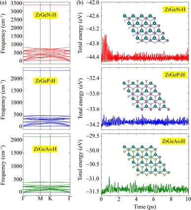 |
| | Fig. 2 (a) The calculated phonon spectra and (b) AIMD results for the total energy to simulation time at 300 K of ZrGeZ3H monolayers. | |
The obtained values of cohesive energy (Ecoh) are listed in Table 1. All three ZrGeZ3H monolayers exhibit negative Ecoh and the ZrGeN3H system has the highest cohesive energy value. This indicates that the ZrGeN3H is the most energetically stable compared to the other two monolayers. It is known that N has a smaller atomic radius than P and As, thus the bond length in the ZrGeN3H monolayer is smaller than that in the ZrGeP3H and ZrGeAs3H, leading to the highest interatomic bond strength in the ZrGeZ3H among the three investigated structures.
Additionally, we analyze the structural phases of Janus ZrGeZ3H systems using Raman spectra. An approach that is frequently used to examine the physical properties of materials with crystallographic symmetry is Raman spectroscopy analysis. Raman spectroscopy can be used to determine several properties of the materials, including their stoichiometry, lattice symmetry, electronic structure, and structural phase. Fig. 3 displays the computed Raman spectra of the ZrGeZ3H monolayers. We observe that all three monolayers exhibit relatively intense and sharp Raman peaks. The ZrGeN3H shows the high-intensity Raman peaks at 822, 612, and 462 cm−1. Notably, the most intense peak of the ZrGeZ3H shifts from 822 cm−1 for the ZrGeN3H to lower frequency of 322 cm−1 for the ZrGeP3H and 219 cm−1 for the ZrGeAs3H monolayer. This shift of Raman peaks relates to the increase in atomic mass of the Z atom.
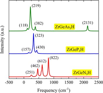 |
| | Fig. 3 Raman spectra of ZrGeZ3H monolayers. The intensity with respect to the frequency. | |
3.2 Electronic properties
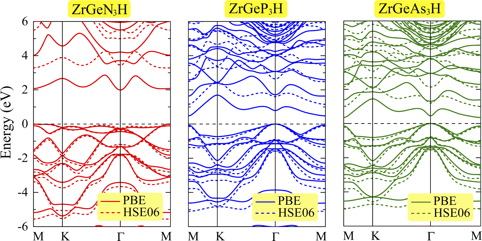
Fig. 4 illustrates the electronic energy band structure of the three ZrGeZ3H monolayers. Herein, we simultaneously use the PBE functional and the HSE06 hybrid functional to evaluate the electronic states of all compounds. Except for the band gap value, both HSE06 and PBE methods give similar results in terms of energy band profile as well as the positions of the conduction band minimum (CBM) and valence band maximum (VBM). All three ZrGeZ3H compounds are indirect semiconductors, but the ZrGeN3H monolayer has a much wider band gap than the other two monolayers. The PBE band gap value gradually decreases from 1.99 to 0.35 eV as Z element goes from N to As. Besides, the band gap value calculated from the HSE06 is larger than that calculated from the PBE method. However, the decreasing tendency of the band gap when Z changes from N to As is still preserved. The HSE06 band gap energy reaches the maximum value of 3.28 eV for the ZrGeN3H monolayer. Table 2 tabulates the calculated results for the band gap energies of the three Janus ZrGeZ3H monolayers.
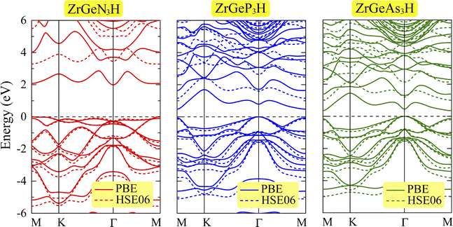 |
| | Fig. 4 Electronic band structure of ZrGeZ3H monolayers at PBE/HSE06 levels. The dashed horizontal line at zero is the Fermi level. | |
Table 2 The elastic coefficients Cij, Young's modulus Y2D and Poisson's ratio ν and piezoelectric coefficients e11, e31, d11, and d31 of the proposed ZrGeZ3H materials
| |
C11 (N m−1) |
C12 (N m−1) |
C66 (N m−1) |
Y2D (N m−1) |
ν |
e11 10−10 C m−1 |
e31 10−10 C m−1 |
d11 (pm V−1) |
d31 (pm V−1) |
| ZrGeN3H |
254.41 |
96.40 |
79.00 |
217.88 |
0.38 |
2.17 |
0.22 |
1.38 |
0.06 |
| ZrGeP3H |
104.12 |
35.12 |
34.50 |
92.26 |
0.34 |
−1.88 |
−0.06 |
−2.72 |
−0.04 |
| ZrGeAs3H |
90.46 |
34.11 |
28.18 |
77.60 |
0.38 |
−2.50 |
−0.19 |
−4.44 |
−0.15 |
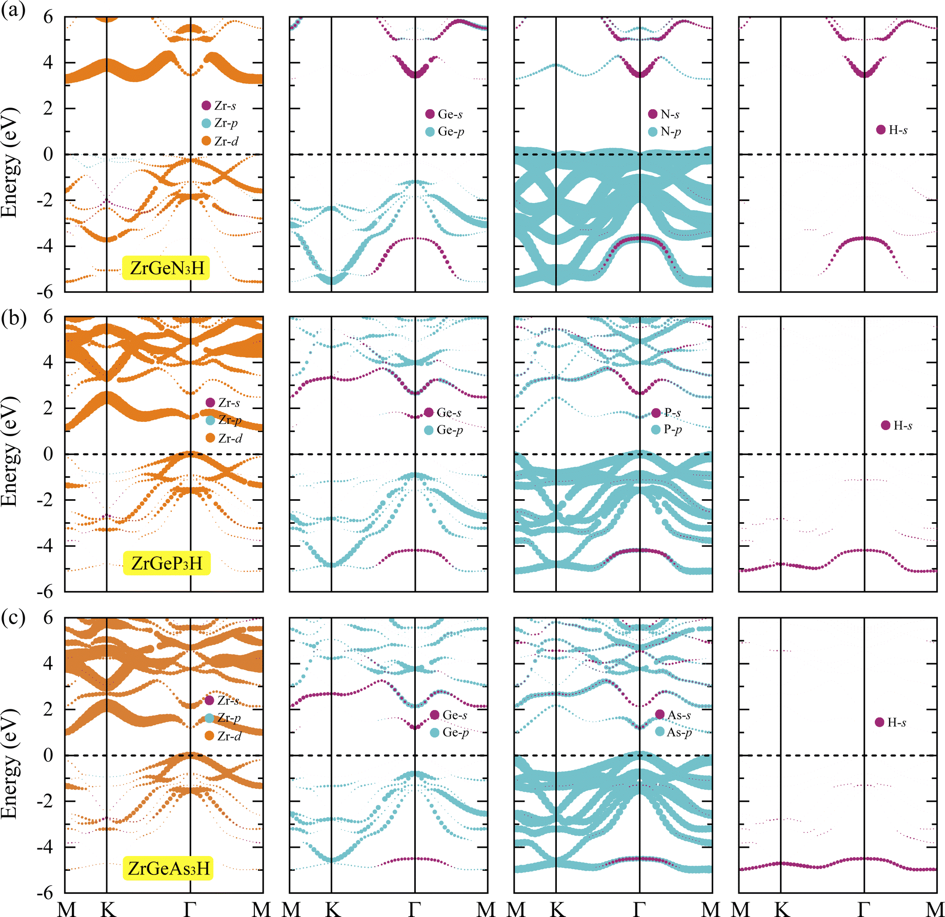
To gain a deeper understanding of the formation of energy band structure from atomic orbitals, we carry out the projected band using the PBE method. Fig. 5 depicts the projected bands of the three Janus ZrGeZ3H configurations at the PBE level. We can see that the d orbital of the Zr element has a major contribution to the construction of the conduction band, and the p orbital of the Z element participates mainly in the formation of the valence band. Besides, the VBM is also made up from the d orbital of the Zr atom.
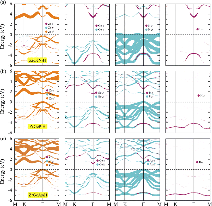 |
| | Fig. 5 Projected band at the PBE level of (a) ZrGeN3H, (b) ZrGeP3H, and (c) ZrGeAs3H monolayers. | |
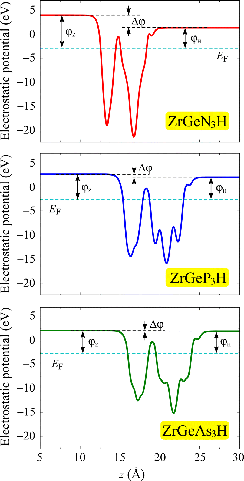
Further, we investigate the work function at the surfaces of the Janus ZrGeZ3H monolayers by evaluating the electrostatic potential. Since the two crystal surfaces are formed by different atoms, the crystal structure is asymmetric with respect to the central atomic layer. Therefore, an intrinsic electric field appears in the perpendicular direction to the planar plane of the material. The magnitude of electric field intensity depends on the electronegativity difference between the different atoms on the two sides of the structure. Therefore, we need to use dipole correction for the electrostatic potential calculation. Fig. 6 depicts the obtained electrostatic potential of the Janus ZrGeZ3H compounds. It is easy to observe that the electrostatic potential possesses an asymmetric shape due to the asymmetric structure of Janus compounds. The work function depends on the Fermi level and the vacuum level by φ = Ev − Ef. This quantity represents the minimum energy that an electron needs to attain to escape from the surface of the crystal. Table 3 shows the calculated work function and vacuum level difference data with the dipole correction. The vacuum level difference between the H and N faces is much higher than between the H and P faces or between the H and As faces. In addition, electrons escape more easily from the H surface than from the Z surface because of the lower work function at the H surface.
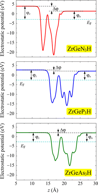 |
| | Fig. 6 Electrostatic potential of ZrGeZ3H monolayers with the dipole correction. The dashed cyan line is set as the Fermi level. | |
Table 3 The PBE/HSE06 bandgap Eg (eV), vacuum level difference Δφ (eV), and work function φ of ZrGeZ3H monolayers
| |
EPBEg |
EHSE06g |
Δφ |
φZ |
φH |
| ZrGeN3H |
1.99 |
3.28 |
2.59 |
6.86 |
4.27 |
| ZrGeP3H |
0.48 |
1.15 |
0.58 |
5.26 |
4.68 |
| ZrGeAs3H |
0.35 |
1.00 |
0.09 |
4.77 |
4.68 |
3.3 Mechanical properties and piezoelectricity
In this section, we discover the mechanical properties and piezoelectricity of the ZrGeZ3H monolayers. Firstly, we report the mechanical properties by calculating the elastic constants, Young's modulus, and Poisson's ratio. For the 2D systems with a hexagonal structure, the elastic constants that need to be calculated are C11 and C12 because the other quantities C22 and C66 are determined through C11 and C12 as C22 = C11 and C66 = (C11 − C12)/2. Table 2 lists the obtained values of the elastic constants, which satisfy the Born–Huang criterion for mechanical stability. Thus, ZrGeZ3H monolayers are predicted to be mechanically stable systems.
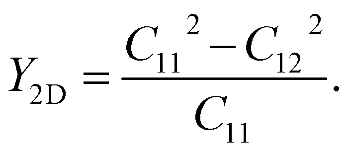
To evaluate the flexibility of the Janus ZrGeZ3H configurations, we calculated their Young's modulus Y2D, which is defined as follows:
| |
 | (2) |
The value of
Y2D changes from 77.60 to 217.88 N m
−1 when the group V element goes from As to N. In other words, when Z element is N, the corresponding monolayer ZrGeN
3H has the highest in-plane stiffness. It can be due to the smallest lattice constant and highest cohesive energy in the ZrGeN
3H monolayer. The
Y2D value of ZrGeN
3H is lower than graphene
37 but higher than MoS
2.
38
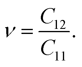
Then, we determine Poisson's ratio of the materials, which represents the mechanical response to the applied stress. Poisson's ratio is calculated from the obtained elastic constants by the following formula:
| |
 | (3) |
The calculated
ν values for all predicted monolayers are also isotropic due to their geometric structure.
Table 2 reveals that the ZrGeP
3H monolayer has the smallest
ν, while the remaining systems have a higher
ν of 0.38. These obtained values of Poisson's ratio are higher than graphene
37 and MoS
2,
38 implying that our considered monolayers are more sensitive to uniaxial strain.
Piezoelectricity is a special effect of the materials; it exhibits efficient performance of converting mechanical energy into electrical energy or vice versa. The piezoelectric response of the material is closely related to the symmetry of the crystal. Specifically, piezoelectric materials should be non-centrosymmetric. Our monolayers belong to the point symmetry group P3m1, which are Janus structures lacking centrosymmetry. Therefore, we can expect that these monolayers exhibit piezoelectric properties.
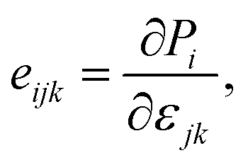
It is well-known that uniaxial deformation causes polarization in the crystal structure of materials. It is the basis for investigating the linear piezoelectric coefficient via piezoelectric stress/strain (eijk/dijk) tensor. The piezoelectric stress/strain tensor is a third-order tensor, which is defined via the surface polarization (P) and strain/stress (εjk/∂σjk) as follows:14
| |
 | (4) |
| |
 | (5) |
where sub-indexes
i,
j,
k ∈ {1, 2, 3} and 1, 2, and 3, respectively, correspond to Cartesian directions
x,
y, and
z.
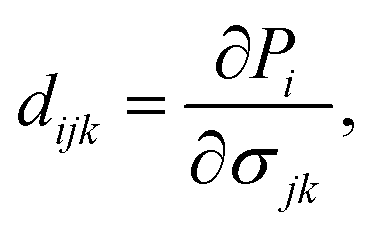
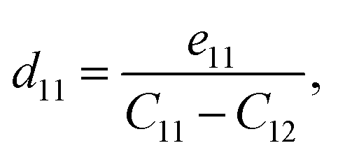
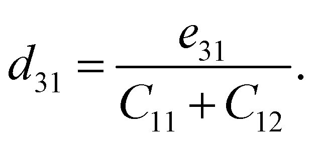
Besides the in-plane piezoelectric coefficients (e11), the Janus ZrGeZ3H monolayers also exhibit out-of-plane piezoelectric response (e31) due to the lack of centrosymmetry. We use density functional perturbation theory to calculate the coefficients eijk by applying uniaxial deformation along the x-axis of orthorhombic supercell. We then evaluate the piezoelectric coefficients dijk through the following relationship:
| |
 | (6) |
| |
 | (7) |
Table 2 summarises the computed piezoelectric coefficients of the ZrGeZ3H configurations. The piezoelectric coefficients e11 and d11 are 2.17 × 10⁻¹⁰, −1.88 × 10⁻¹⁰, −2.50 × 10⁻¹⁰ C m−1 and 1.38, −2.72, −4.44 pm V−1 for the ZrGeN3H, ZrGeP3H and ZrGeAs3H systems, respectively. These results imply that the ZrGeAs3H monolayer exhibits the highest piezoelectric response of all the proposed monolayers. The values of e11 and d11 are comparable to e11 and d11 obtained in MoGeN3H39 and WSiZ3H.40 Additionally, the ZrGeZ3H monolayers also possess the out-of-plane piezoelectric responses. The e31 coefficient reaches the highest value of 0.22 × 10⁻¹⁰ C m−1 for the ZrGeN3H monolayer, while the ZrGeAs3H monolayer exhibits the highest magnitude d31 of −0.15 pm V−1. The obtained e31 and d31 are similar to those reported in the Janus WSiZ3H system.40
3.4 Transport properties
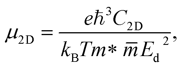
At last, we study the mobility of carriers and related transport features of our Janus monolayers. The magnitude of the carrier mobility of 2D nanostructures is an essential factor for the nanoelectronics and optoelectronics. We can estimate the carrier mobility in 2D semiconductors based on the deformation potential (DP) method. According to this theory, the room temperature μ2D of the three systems is determined by the following equation:| |
 | (8) |
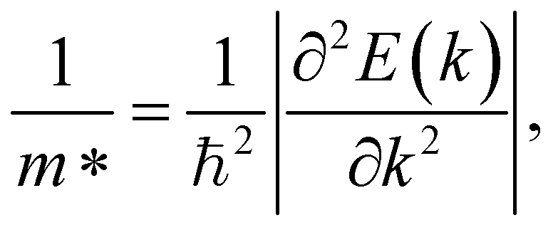
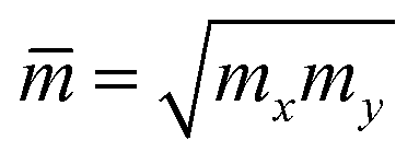
where m* and  are the effective mass and average effective mass, respectively. T, e, ℏ, and kB indicate, respectively, the temperature, the elementary charge, the reduced Planck constant, and the Boltzmann constant. Ed and C2D are the deformation potential constant and elastic modulus, respectively. The effective masses of holes/electrons are defined as:
| |
 | (9) |
Here E(k) is the energy corresponding to wave vector k. Table 4 shows the effective mass achieved for the ZrGeZ3H monolayers. The m* values show the same trend in all three Janus systems. Taking the ZrGeN3H system as an example, the effective mass of electrons and holes in the x direction is smaller than that in the y direction, and the electron mass is smaller than the hole mass along a given direction. This can significantly affect the mobility of carriers. The hole mass in the Janus ZrGeN3H monolayer is the largest among the three monolayers, which is related to the electronic band structure as shown in Fig. 4.
Table 4 Effective mass of carriers m* (in units of free electron mass m0), 2D elastic modulus C2D (Nm−1), DP constants Ed (eV), and carrier mobility μ (cm2 V−1 s−1) of ZrGeZ3H monolayers along the x and y axes
| |

|

|
C2Dx |
C2Dy |
Edx |
Edy |
μx |
μy |
| Electron |
ZrGeN3H |
0.26 |
0.30 |
140.59 |
140.59 |
−10.51 |
−10.50 |
369.81 |
320.17 |
| |
ZrGeP3H |
0.27 |
0.63 |
68.77 |
68.80 |
−1.99 |
−1.86 |
3408.37 |
1665.96 |
| |
ZrGeAs3H |
0.27 |
0.62 |
60.06 |
60.12 |
−1.80 |
−1.71 |
3639.20 |
1734.14 |
| Hole |
ZrGeN3H |
1.35 |
2.34 |
140.59 |
140.59 |
−5.78 |
−6.61 |
37.44 |
16.49 |
| |
ZrGeP3H |
0.87 |
1.08 |
68.77 |
68.80 |
−4.88 |
−4.98 |
72.53 |
56.20 |
| |
ZrGeAs3H |
0.81 |
0.95 |
60.06 |
60.12 |
−4.62 |
−4.72 |
84.34 |
68.96 |
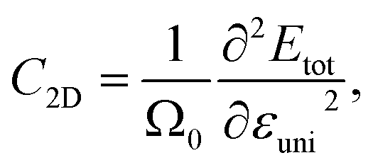
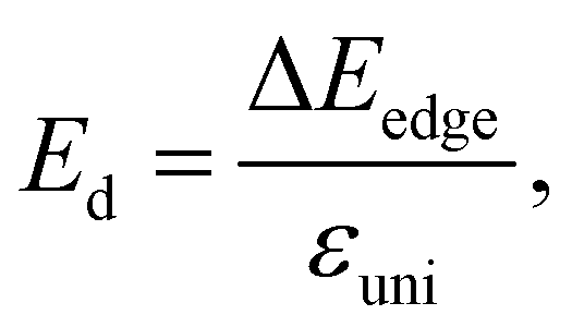
Besides the effective mass, the deformation potential constant and elastic modulus also decide the value of carrier mobility, and they are expressed as follows:
| |
 | (10) |
| |
 | (11) |
where Δ
Eedge is the shift of band-edge with respect to the vacuum level caused by the uniaxial strain.
Etot and
Ω0 refer to the total energy and area of the supercell at equilibrium.
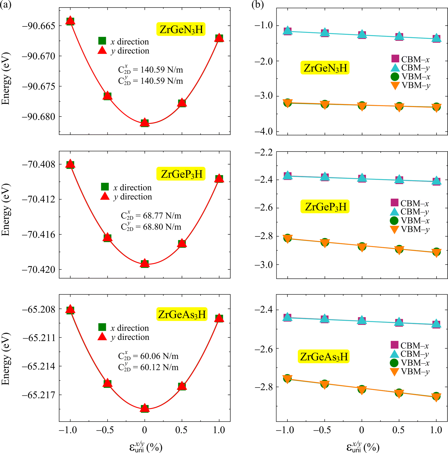
Fig. 7 plots the energy shifting and band-edge positions as a function of the uniaxial strain along two transport directions. The achieved values of
Ed and
C2D are shown in
Table 4. We can realize that the ZrGeN
3H monolayer has larger |
Ed| and
C2D than the other monolayers.
 |
| | Fig. 7 The energy shifting (a) and band-edge positions as a function of the uniaxial strain of ZrGeZ3H monolayers along x and y directions. The solid lines are the fitting curves. | |
Then we calculate the carrier mobility of three Janus ZrGeZ3H monolayers based on the relevant parameters, and the calculated results are presented in Table 4. It can be seen that the electron mobility varies from 320.17 to 3639.20 cm2 V−1 s−1, while the hole mobility has a much smaller magnitude, from 16.49 to 84.34 cm2 V−1 s−1. Thus, there is a significant difference in the mobility between electrons and holes in the given monolayers. The carrier mobility is also anisotropy in the different transport directions. The electron/hole mobilities exhibit different values along the two in-plane directions. As shown in Table 4, the ZrGeAs3H and ZrGeP3H monolayers have very high electron mobility of 3639.20 and 340.378 cm2 V−1 s−1, respectively. Our calculated results demonstrate that the ZrGeN3H monolayer exhibits lower electron mobility than that in ZrGeAs3H and ZrGeP3H monolayers. This is due to the high value of the deformation potential constant (absolute value |Ed|) of ZrGeN3H monolayer as listed in Table 4. The high |Ed| of ZrGeN3H suggests that the influence of uniaxial strains on its band-edge positions is significant. These values are one order of magnitude higher than the electron mobility in the conventional material MoS2.41 This suggests that our predicted monolayers have promising applications in electronic components.
4 Conclusion
To summarize, we have conducted a theoretical analysis based on the fundamentals of DFT calculations to explore the structural stability, electronic features, piezoelectricity, Raman response, and carrier mobility of the 2D Janus ZrGeZ3H monolayers. The phonon dispersion spectra, AIMD simulation, cohesive energy, and elastic coefficient calculations confirm the structural stability of these systems. The computed band structures reveal that all proposed configurations are indirect semiconductors with band gaps ranging from 1.00 to 3.28 eV at the HSE06 level. For each Janus system, the work function at the H surface is smaller than at the Z surface. The obtained projected bands of the three ZrGeZ3H systems indicate that the d orbital of the Zr element contributes mainly to the construction of the conduction band, while the p orbital of Z element has numerous participation in the formation of the valence band. Notably, we obverse the coexistence of in-plane and out-of-plane piezoelectric coefficients in all three monolayers. In addition, the carrier mobilities of electrons and holes along transport directions are anisotropic. It is found that the electron mobility is high up to 3639.20 and 3408.37 cm2 V−1 s−1 for ZrGeAs3H and ZrGeP3H systems, respectively. Our findings reveal that the 2D Janus ZrGeZ3H structures are suitable candidates for piezoelectric and electric applications.
Data availability
The data that support the findings of this study are available upon reasonable request from the corresponding author.
Conflicts of interest
There are no conflicts of interest to declare.
Acknowledgements
This research is funded by Hue University under project number DHH2023-04-207. Khanh V Hoang acknowledges Phenikaa University for providing HPC computational resources.
References
- J. Xin, Y. Zheng and E. Shi, Appl. Phys. Lett., 2007, 91, 112902 CrossRef.
- M. N. Blonsky, H. L. Zhuang, A. K. Singh and R. G. Hennig, ACS Nano, 2015, 9, 9885–9891 CrossRef CAS.
- Y. Chen, J. Liu, J. Yu, Y. Guo and Q. Sun, Phys. Chem. Chem. Phys., 2019, 21, 1207–1216 RSC.
- M. Dragoman, A. Dinescu and D. Dragoman, Phys. Status Solidi A, 2019, 216, 1800724 CrossRef.
- Z. Liu, H. Wang, J. Sun, R. Sun, Z. F. Wang and J. Yang, Nanoscale, 2018, 10, 16169–16177 RSC.
- T. Tan, X. Jiang, C. Wang, B. Yao and H. Zhang, Adv. Sci., 2020, 7, 2000058 CrossRef CAS.
- F. R. Fan, R. Wang, H. Zhang and W. Wu, Chem. Soc. Rev., 2021, 50, 10983–11031 RSC.
- Y. Zhu, L. Peng, Z. Fang, C. Yan, X. Zhang and G. Yu, Adv. Mater., 2018, 30, 1706347 CrossRef.
- D. Li, Y. Gong, Y. Chen, J. Lin, Q. Khan, Y. Zhang, Y. Li, H. Zhang and H. Xie, Nano-Micro Lett., 2020, 12, year Search PubMed.
- H. Zhu, Y. Wang, J. Xiao, M. Liu, S. Xiong, Z. J. Wong, Z. Ye, Y. Ye, X. Yin and X. Zhang, Nat. Nanotechnol., 2014, 10, 151–155 CrossRef PubMed.
- C. Zhang, Y. Nie, S. Sanvito and A. Du, Nano Lett., 2019, 19, 1366–1370 CrossRef CAS.
- J. Zhang, S. Jia, I. Kholmanov, L. Dong, D. Er, W. Chen, H. Guo, Z. Jin, V. B. Shenoy, L. Shi and J. Lou, ACS Nano, 2017, 11, 8192–8198 CrossRef CAS.
- L. Zhang, Z. Yang, T. Gong, R. Pan, H. Wang, Z. Guo, H. Zhang and X. Fu, J. Mater. Chem. A, 2020, 8, 8813–8830 RSC.
- K.-A. N. Duerloo, M. T. Ong and E. J. Reed, J. Phys. Chem. Lett., 2012, 3, 2871–2876 CrossRef CAS.
- W. Li and J. Li, Nano Res., 2015, 8, 3796–3802 CrossRef CAS.
- R. Fei, W. Li, J. Li and L. Yang, Appl. Phys. Lett., 2015, 107, 173104 CrossRef.
- Y. Guo, S. Zhou, Y. Bai and J. Zhao, Appl. Phys. Lett., 2017, 110, 163102 CrossRef.
- S.-D. Guo, X.-S. Guo, Z.-Y. Liu and Y.-N. Quan, J. Appl. Phys., 2020, 127, year Search PubMed.
- M. Yagmurcukardes, C. Sevik and F. M. Peeters, Phys. Rev. B, 2019, 100, 045415 CrossRef CAS.
- M. Yagmurcukardes and F. M. Peeters, Phys. Rev. B, 2020, 101, 155205 CrossRef CAS.
- T. V. Vu, H. V. Phuc, A. I. Kartamyshev and N. N. Hieu, Appl. Phys. Lett., 2023, 122, 061601 CrossRef CAS.
- D. Bezzerga, E.-A. Haidar, C. Stampfl, A. Mir and M. Sahnoun, Nanoscale Adv., 2023, 5, 1425–1432 RSC.
- Y.-L. Hong, Z. Liu, L. Wang, T. Zhou, W. Ma, C. Xu, S. Feng, L. Chen, M.-L. Chen, D.-M. Sun, X.-Q. Chen, H.-M. Cheng and W. Ren, Science, 2020, 369, 670–674 CrossRef CAS PubMed.
- L. Wang, Y. Shi, M. Liu, A. Zhang, Y.-L. Hong, R. Li, Q. Gao, M. Chen, W. Ren, H.-M. Cheng, Y. Li and X.-Q. Chen, Nat. Commun., 2021, 12, 2361 CrossRef CAS PubMed.
- V. T. T. Vi, T. P. T. Linh, C. Q. Nguyen and N. N. Hieu, Adv. Theory Simul., 2022, 5, 2200499 CrossRef CAS.
- N. T. Hiep, N. P. Q. Anh, H. V. Phuc, C. Q. Nguyen, N. N. Hieu and V. T. T. Vi, Phys. Chem. Chem. Phys., 2023, 25, 8779–8788 RSC.
- R. Sibatov, R. Meftakhutdinov and A. Kochaev, Appl. Surf. Sci., 2022, 585, 152465 CrossRef CAS.
- G. Kresse and J. Furthmüller, Phys. Rev. B: Condens. Matter Mater. Phys., 1996, 54, 11169–11186 CrossRef CAS PubMed.
- G. Kresse and J. Furthmüller, Comput. Mater. Sci., 1996, 6, 15–50 CrossRef CAS.
- J. P. Perdew, K. Burke and M. Ernzerhof, Phys. Rev. Lett., 1996, 77, 3865 Search PubMed.
- J. Heyd, G. E. Scuseria and M. Ernzerhof, J. Chem. Phys., 2003, 118, 8207 CrossRef CAS.
- A. Togo, L. Chaput and I. Tanaka, Phys. Rev. B, 2015, 91, 094306 CrossRef.
- S. Grimme, J. Antony, S. Ehrlich and H. Krieg, J. Chem. Phys., 2010, 132, 154104 CrossRef PubMed.
- M. Yagmurcukardes, F. M. Peeters and H. Sahin, Phys. Rev. B, 2018, 98, 085431 CrossRef CAS.
- S. Nosé, J. Chem. Phys., 1984, 81, 511 CrossRef.
- J. Bardeen and W. Shockley, Phys. Rev., 1950, 80, 72 CrossRef CAS.
- C. Lee, X. Wei, J. W. Kysar and J. Hone, Science, 2008, 321, 385–388 CrossRef CAS PubMed.
- J. Kang, H. Sahin and F. M. Peeters, Phys. Chem. Chem. Phys., 2015, 17, 27742–27749 Search PubMed.
- X. Cai, G. Chen, R. Li, Z. Pan and Y. Jia, J. Mater. Chem. C, 2024, 4682 RSC.
- T. V. Vu, B. D. Hoi, A. I. Kartamyshev and N. N. Hieu, J. Appl. Phys., 2024, 135, 074301 Search PubMed.
- B. Radisavljevic, A. Radenovic, J. Brivio, V. Giacometti and A. Kis, Nat. Nanotechnol., 2011, 6, 147–150 CrossRef CAS PubMed.
|
| This journal is © The Royal Society of Chemistry 2024 |
Click here to see how this site uses Cookies. View our privacy policy here. 
 Open Access Article
 This Open Access Article is licensed under a Creative Commons Attribution-Non Commercial 3.0 Unported Licence
 ab,
Vo T. T. Vi
ab,
Vo T. T. Vi

 are the effective mass and average effective mass, respectively. T, e, ℏ, and kB indicate, respectively, the temperature, the elementary charge, the reduced Planck constant, and the Boltzmann constant. Ed and C2D are the deformation potential constant and elastic modulus, respectively. The effective masses of holes/electrons are defined as: