DOI:
10.1039/D4RA03695F
(Paper)
RSC Adv., 2024,
14, 24066-24081
Solar power conversion: CuI hole transport layer and Ba3NCl3 absorber enable advanced solar cell technology boosting efficiency over 30%
Received
19th May 2024
, Accepted 8th July 2024
First published on 1st August 2024
Abstract
Researchers are becoming more interested in novel barium-nitride-chloride (Ba3NCl3) hybrid perovskite solar cells (HPSCs) due to their remarkable semiconductor properties. An electron transport layer (ETL) built from TiO2 and a hole transport layer (HTL) made of CuI have been studied in Ba3NCl3-based single junction photovoltaic cells in a variety of variations. Through extensive numerical analysis using SCAPS-1D simulation software, we investigated elements such as layer thickness, defect density, doping concentration, interface defect density, carrier concentration, generation, recombination, temperature, series and shunt resistance, open circuit voltage (VOC), short circuit current (JSC), fill factor (FF), and power conversion efficiency (PCE). The study found that the HTL CuI design reached the highest PCE at 30.47% with a VOC of 1.0649 V, a JSC of 38.2609 mA cm−2, and an FF of 74.78%. These findings offer useful data and a practical plan for producing inexpensive, Ba3NCl3-based thin-film solar cells.
1. Introduction
The development of perovskite materials for potential incorporation into efficient solar cell technologies has resulted in significant advancements in photovoltaics.1 In photovoltaics, perovskite materials have made substantial progress and are predicted to provide high-efficiency solar cell technology substitutes.2,3 More specifically, the unique and intriguing structural, electrical, and optical properties of inorganic perovskites have garnered a lot of interest. Several A3MX3 (where a cation is indicated by A, M refers to a metal ion, and X is a halogen anion) group perovskites have recently surfaced as outstanding candidates among these materials.4–8 While hybrid organic–inorganic perovskite solar cells (PSCs) have minimal trap presence, excellent light absorption, superior mobility of charge carriers, reduced binding energy for excitons, and an extended lifespan for charge carriers, these features significantly improve PV performance.9–12 But the main problems with the extensive industrial use of organic cations are their thermal instability and volatility.13,14 Certain materials, such as methylammonium lead iodide (MAPbI3) and formamidinium lead iodide (FAPbI3),15 have disadvantages such instability in ambient settings, lead toxicity, and difficulties with scaling in large-scale manufacture. These problems impair their long-term effectiveness in real-world applications as well as their commercial feasibility.
The exceptional properties of perovskites, such as their high mobility of electrons and ions, changeable bandgap, and efficient absorption of light, render them ideal for a variety of uses, such as energy storage, photovoltaic electronic devices, and catalysis.16 Scientists are interested in perovskite materials because they may be able to produce extremely efficient photovoltaic solar cells.17 Ba3NCl3 perovskite offers several advantages in solar cell performance. It exhibits better thermal and chemical stability compared to organic–inorganic perovskites, which enhances the lifespan of solar cells. It has a suitable bandgap for efficient light absorption, which can be optimized for improved solar energy conversion. Being lead-free, it addresses environmental and health concerns associated with lead-based perovskites. It has a better absorption coefficient compare to others perovskites. With an adjustable band gap (1.20 eV), exceptional compositional stability, and thermal stability, inorganic Ba3NCl3 perovskites emerged as a promising absorber for use in the creation of high-performance perovskite solar cells.18 Perovskite solar cells have garnered a lot of interest in the last few years because of their improved power conversion efficiency (PCE), which has surpassed 26%.19,20 Thus, to stabilize Ba3NCl3 in the black phase, several techniques like doping, decreasing grain size, adjusting the value of tolerance factor, or modifying surface energy are applied. In addition, the doping method—which stabilizes the black phase in Ba3NCl3 by introducing the appropriate element ions—is frequently employed. It is possible to improve photovoltaic performance by adding beneficial element ions to the Ba3NCl3 host lattices and choosing the right hole transport layer (HTL) and electron transport layer (ETL).21,22 The VOC can be enhanced by interlayer insertion between Ba3NCl3 and the back contact by lowering the unanticipated level of Fermi trapping at the absorber–metal interaction that inhibits carriers having bends in the band.23 By utilizing a highly doped p-type semiconductor as the hole transport layer (HTL) at the back side of the, this pinning effect can be avoided.24 Therefore, by creating a p+–p junction with a high electric field, the absorber layer can limit the loss of carrier recombination at the HTL/absorber contact.25 The transmission of holes can also be enhanced by a strongly doped HTL (p+ type) that has a little offset of valence band (VBO). Research is being done to develop an HTL between the back contact and the absorber.26,27 The goal of the research is to create an HTL material, such as CuI, with improved electrical and optical properties.28 Thus far, the only reports of improved PV performance have been of combined high-efficiency Ba3NCl3 absorber setups with Al/FTO/TiO2/Ba3NCl3/CuI/Ni design.
A new device combination featuring Al/FTO/TiO2/Ba3NCl3/CuI/Ni is utilized in this study. We obtained the highest PCE at 30.47%, with a VOC of 1.0649 V, a JSC of 38.2609 mA cm−2, and an FF of 74.78% using the Al/FTO/TiO2/Ba3NCl3/CuI/Ni structure. These results are superior than those of other reported Ba3NCl3 based devices, which is the novelty of this work. This suggested Ba3NCl3-based solar cell shows exceptional maintenance efficiency when compared to conventional thin-film solar cells, demonstrating Ba3NCl3's appeal as a solar energy system material while removing potential toxicity issues.
In this study, a detailed analysis and investigation of the photovoltaic performance of Ba3NCl3 absorber-based double-heterojunction solar cells with and without HTL have been conducted. Analyzing the effects of many metals as front and rear contacts was first assumed to identify the least resistive junction at the metal–semiconductor interface. The work function of the materials used in the contacts is crucial because it determines the efficiency of charge extraction and transport. Proper alignment of the energy levels between different layers ensures minimal energy barriers for charge carriers, leading to efficient operation of the solar cell. Aluminum (Al) has been proposed as the optimal choice for the front contact, while nickel (Ni) has been recommended for the rear contact.29 Subsequently, the photovoltaic (PV) acts of innovative Ba3NCl3 absorber-based cell structures for HTL of CuI with ETL of TiO2 were computed for various working temperatures, thicknesses of layer, densities for doping, total defect as well as interface defect densities, series and shunt resistance, including rate of carrier generation and recombination, using SCAPS-1D simulator software to determine quantum efficiency (QE) and the current density–voltage (J–V).
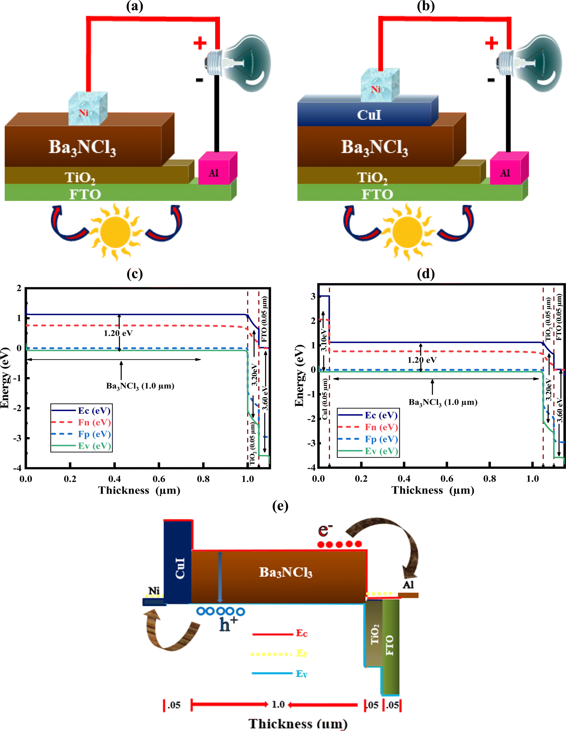
2. Device construction and simulation techniques
The suggested Al/FTO/TiO2/Ba3NCl3/CuI/Ni photovoltaic cells have been modelled using the one-dimensional Solar Cell Capacitance Simulator (SCAPS) tool. A one-dimensional solar cell modelling tool called SCAPS (a Solar Cell Capacitance Simulator) was created at the University of Gent, Belgium's Department of Electronics and Information Systems (ELIS). Basic equations were solved to predict and systematically assess both structures: Fig. 1a and b simultaneously display equations of continuity for both holes and electrons, alongside equations describing the electrostatic potential, all under conditions of steady-state without HTL and with HTL symmetrical structures. The layers that make up the n+–n–p–p+ structure are as follows: a 0.05 μm thick layer of FTO; a 0.05 μm thick layer of n-type TiO2 ETL; a 1.0 μm thick layer of Ba3NCl3 absorber; and a 0.05 μm thick layer of p+-type HTL CuI with Ni and Al serving as the back and front metal electrodes. Fig. 1c and d show the energy band diagrams with and without HTL concurrently. The band alignment for all layers of Al/FTO/TiO2/Ba3NCl3/CuI/Ni structure is shown in Fig. 1(e). The positions of quasi-Fermi states Fn and Fp under illumination confirm the production of electron–hole pairs in the gadget. The offset between absorber CB and VB confirms that electron–hole pairs have formed inside the device. The difference in work function (WF) between the absorber and transmission layers is responsible for the offset that is seen. Light generated at the absorber/ETL interface is separated with the help of integrated voltage and related electrical fields. The fundamental equations of one-dimensional semiconductors were solved with the SCAPS-1D simulator in order to get the PV parameters. Numerous input and output parameters exist in this work, including:
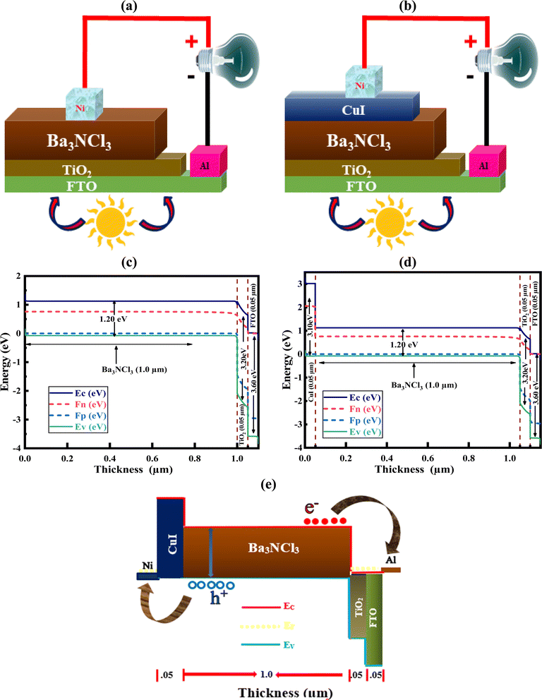 |
| | Fig. 1 The Device structures (a) without HTL, (b) with HTL, energy band diagram (c) without HTL, (d) with HTL CuI, and (e) band alignment of Al/FTO/TiO2/Ba3NCl3/CuI/Ni. | |
2.1. Efficiency
The efficiency of solar cell materials is defined as the percentage of solar radiation that is transformed into electrical energy, indicating how well they can convert sunlight into electricity. Greater power output per unit area of a solar cell is indicated by high efficiency.
2.2. Short circuit current
In solar cell materials, the highest current produced when the cell is exposed to light and its terminals are shorted is known as the short circuit current (ISC). It is a crucial factor in determining the efficiency of the cell since it represents its capacity to produce charge carriers.
2.3. Open circuit voltage
The highest voltage that a solar cell can produce while there is no current flowing through the circuit is known as the open circuit voltage (VOC) in sun cell materials. It symbolizes the potential difference between the cell's positive and negative terminals when it is not in circuit.
2.4. Fill factor
The ratio of the actual maximum attainable power to the theoretical power if both current and voltage were at their maximum is known as the fill factor (FF) in solar cell materials. It is a crucial factor in determining a solar cell's effectiveness since it indicates the calibre of the material and construction used in the cell.
2.5. Electron affinity
The energy change that occurs when an electron is introduced to a neutral atom or molecule is known as electron affinity and is commonly expressed in electron volts (eV) in solar cell materials. It affects how well charges are separated and transferred within the solar cell.
2.6. Band gap
The energy differential between the bottom of the conduction (free electron flow) and the top of the valence (outer electron) band is referred to as the band gap.
2.7. Density of states
The amount of electronic states that are accessible in a material at each energy level is described by the density of states (DOS) in solar cell materials. It is essential for figuring out how well charge carrier recombination and generation work together, which affects the solar cell's overall performance.
2.8. Dielectric permittivity
The ability of a material to polarize in response to an electric field, which affects charge separation and transport, is measured by its dielectric permittivity in solar cell materials. Dielectric permittivity influences solar cell performance by enhancing internal electric fields, reducing charge recombination, and improving charge carrier mobility, leading to higher efficiency. It affects the optical properties, improving light absorption and reducing reflection losses. Proper dielectric permittivity aids in better impedance matching and capacitance management, ensuring efficient power transfer. It also affects band alignment and stability, optimizing energy levels and device longevity. In essence, optimizing dielectric permittivity is crucial for maximizing solar cell efficiency and stability.
2.9. Acceptor and donar density
The concentration of acceptor impurities, which produce holes (positive charge carriers), usually in p-type semiconductors, is referred to as acceptor density in solar cell materials. The concentration of donor impurities, which are typically found in n-type semiconductors, that supply free electrons (negative charge carriers) is referred to as donor density.
2.10. Electron and hole mobility
The ease with which electrons and holes—positive charge carriers—can travel through various materials used in solar cells is referred to as electron and hole mobility. Improved charge transport characteristics, which are essential for effective solar cell operation, are indicated by higher mobilities.
2.11. Interface defect density
The number of flaws per unit area at the junctions between different layers in solar cell materials is known as the interface defect density. These imperfections have the potential to trap charge carriers and lower the efficiency of the cell. It is a crucial factor affecting the stability and overall performance of the solar cell.
2.12. Defect density
The number of structural flaws per unit area or volume that can negatively impact the performance of the cell by obstructing charge carrier flow is referred to as defect density in solar cell materials. Higher efficiency and improved overall performance of the solar cells are usually the result of lower fault levels.
The set of equations includes Poisson's equation alongside the continuity equations for both electrons and holes, followed by expressions for drift and diffusion drift denoted by eqn (1)–(5).30,31
| |
 | (1) |
| |
 | (2) |
| |
 | (3) |
| |
 | (4) |
| |
 | (5) |
The subsequent information has been gathered from available sources in addition to the experiment results and implemented as simulation variables: dielectric permittivity εr, thickness of layers (nm), energy gap of bands Eg (eV), the valence band density NV (cm−3), affinity of electron χ (eV), density of the conduction band NC (cm−3), mobility of hole μh (cm2 V−1 s−1), donor density ND (cm−3), mobility of electron μn (cm2 V−1 s−1), recombination coefficient (cm3 s−1), and acceptor density NA (cm−3) were taken into account. An overview of all these simulating parameters is provided in Tables (1 as well as 2) for the anticipated heterostructures. For TiO2 and CuI, the authors have chosen and verified the absorption coefficients from credible literature, ensuring future simulations beyond a reasonable doubt. By using SCAPS 1D software, we have added neutral type bulk defect densities in all layers to this study. These defects are distributed throughout the volume of the absorber material. They represent intrinsic defects within the bulk of the material that affect bulk recombination. Whenever an experimental version of the proposed device is produced, the limitations on design methodology, manufacturing, environmental impacts, and high precision measurement might lead to a notable discrepancy between simulation and experiment.
Table 1 Specifications for the absorber layer, FTO, ETL, and HTL layer
| Parameters |
FTO32 |
TiO2 (ref. 33) |
Ba3NCl3 (ref. 18) |
CuI28 |
| Thickness (nm) |
50 |
50 |
1000 |
50 |
| Band gap, Eg (eV) |
3.60 |
3.20 |
1.20 |
3.10 |
| Electron affinity, χ (eV) |
4.5 |
3.9 |
4.0 |
2.1 |
| Dielectric permittivity (relative), εr |
10 |
9 |
5.32 |
6.5 |
| CB effective density of states, NC (cm−3) |
2 × 10¹⁸ |
1 × 10¹⁹ |
3.96 × 10¹⁸ |
2.5 × 10¹⁹ |
| VB effective density of states, NV (cm−3) |
1.8 × 10¹⁹ |
1 × 10¹⁹ |
1.83 × 10¹⁹ |
2.5 × 10¹⁹ |
| Electron mobility, μn (cm2 V−1 s−1) |
100 |
200 |
50 |
100 |
| Hole mobility, μh (cm2 V−1 s−1) |
20 |
10 |
50 |
43.9 |
| Shallow uniform acceptor density, NA (cm−3) |
0 |
0 |
1 × 10¹⁸ |
1 × 10¹⁸ |
| Hallow uniform donor density, ND (cm−3) |
1 × 10¹⁸ |
1 × 10¹⁷ |
0 |
0 |
| Defect density, Nt (cm−3) |
1 × 10¹⁴ |
1 × 10¹⁴ |
1 × 10¹² |
1 × 10¹⁴ |
Table 2 Data for interface parameters used in the Al/FTO/TiO2/Ba3NCl3/CuI/Ni solar cell
| Parameter |
Ba3NCl3/TiO2 |
CuI/Ba3NCl3 |
| Type of defect |
Neutral |
Neutral |
| σh (cm2) |
1 × 10¹⁹ |
1 × 10¹⁹ |
| σe (cm2) |
1 × 10¹⁹ |
1 × 10¹⁹ |
| Total density of defect |
1010 |
1010 |
| Er |
0.6 |
0.6 |
| Working temperature (K) |
300 |
300 |
| Energetic distribution |
Single |
Single |
3. Result and discussion
3.1. Thickness optimization of the absorber and ETL layers
Fig. 2(a) illustrates how varying the depth of the absorber layer between 300 and 3000 nm affects the recommended devices' capacity to maximize performance, while keeping other parameters as stated in Table 1. Significant increases in absorber layer thickness are seen in both carrier production and recombination rates. With an increase in absorber thickness, the VOC of the without HTL group was nearly constant at 0.9764–0.9777 V, whereas the with HTL group saw a modest drop in VOC, from 1.10561–1.0296 V. However, because of increased spectrum absorption,34 especially at longer wavelengths, the JSC increases with larger absorber layers. JSC values have significantly increased both with and without HTL: with HTL, they have increased from 32.337 to 38.877 mA cm−2, while without HTL, they have increased from 32.331 to 38.868 mA cm−2. These differences between JSC and VOC indicate a tendency that is consistent with research from papers.35–37 The FF is relatively stable at 74.78% for with HTL and 73.27% for without HTL. For both with HTL and without HTL, PCE grew as absorber thickness increased. When the length of charge carrier diffusion and thickness of absorber layer are equivalent, PSC performance is demonstrated to peak. It is evident from Fig. 2(a) that altering the thickness of the absorber layer has a major impact on the overall performance of PV systems. It is clear that we operate at our best when Ba3NCl3 is thicker than 1000 nm. Performance does not significantly increase or, in certain circumstances, decreases as thickness increases over ∼1000 nm. As a result, we have decided that the optimal thickness for the absorber to be 1000 nm. This led to the following results: VOC of 0.9803 and 1.0697 V, JSC of 38.2534 and 38.2609 mA cm−2, FF of 73.27 and 74.78%, and PCE of 27.48 and 30.47% for both without and with HTL structures.
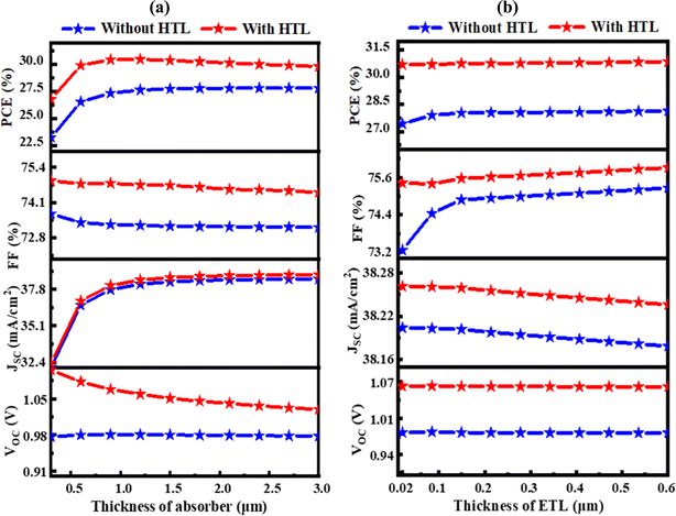 |
| | Fig. 2 The thickness variation effect of (a) absorber Ba3NCl3 and (b) ETL TiO2 layers on PV parameters of VOC, PCE, JSC, and FF. | |
As seen in Fig. 2(b), the thickness of the ETL layer can significantly affect the performance of PV devices. Buffer layers help to move charge carriers from the absorber layer to the electrode more easily, which increases the stability and efficiency of PV devices. Several properties of PV devices, like as light absorption, charge carrier recombination, and interlayer contact resistance, can be influenced by the thickness of the ETL layer. Wider band gap smaller layers efficiently transport nearly all incident photons to the Ba3NCl3 absorber layer, improving light absorption in the cells. Despite the ETL layer being thicker, the VOC remained nearly constant at 0.96 and 1.03 V, respectively, with and without HTL. However, there was a modest fall in the JSC values for both the without HTL and with HTL groups, with declines of 38.2538 to 38.2285 mA cm−2 and 38.2611 to 38.2358 mA cm−2, respectively. The changing thickness of the ETL layer has minimal impact on JSC as the layer remains within an optimal range as shown in Fig. 2(b), ensuring efficient electron extraction and minimal recombination. As the ETL is neither too thin to cause leakage nor too thick to hinder transport, JSC remains relatively stable. Proper ETL design maintains effective charge collection across varying thicknesses. Additionally, there was some variation in the FF values between without HTL (73.25% to 75.26%, respectively). At 74.78%, the FF for with HTL was essentially stable. The PCE for the absence of HTL increased slightly, from 27.43% to 28.13. The PCE for with HTL remained relatively consistent at 30.47% as the thickness of the ETL layer grew. As a result of the ETL layer's thickness modifications, PCE, JSC, FF, and VOC have not significantly altered, as shown in Fig. 2(b). This suggests that there is no appreciable difference in the thickness of the ETL. In order to lower the cost of production, we have decided that 50 nm is the ideal thickness for the ETL layer. Because producing something that is practically thinner than 50 nm is nearly impossible. The output values of the suggested devices from this work are compared to those from earlier works in Table 3.
Table 3 A comparison between this work's PV parameters versus those from earlier studies
| Structures |
VOC (V) |
JSC (mA cm−2) |
FF (%) |
PCE (%) |
Ref. |
| FTO/TiO2/Ba3NCl3 |
0.980 |
38.2534 |
73.27 |
27.48 |
This work |
| FTO/TiO2/Ba3NCl3/CuI |
1.064 |
38.2609 |
74.78 |
30.47 |
This work |
| FTO/SnS2/Sr3SbI3 |
0.93 |
34.67 |
87.31 |
28.05 |
38 |
| FTO/SnS2/Sr3PI3 |
0.92 |
34.65 |
34.65 |
28.15 |
39 |
| FTO/SnS2/Ba3NCl3 |
0.94 |
38.26 |
79.91 |
28.81 |
18 |
| Al/FTO/WS2/RbPbBr3/Au |
0.8967 |
34.5466 |
79.23 |
24.56 |
40 |
| FTO/SnS2/Sr3NCl3 |
1.24 |
16.79 |
86.44 |
18.11 |
18 |
| CH3NH3PbI3/CuSCN |
1.0 |
23.12 |
83.56 |
19.33 |
41 |
| CIGS/CH3NH3PbI3 |
0.84 |
27.2 |
84 |
19.29 |
42 |
| n-TiO2/i-CH3NH3SnBr3/p-NiO |
0.80 |
31.88 |
84.89 |
21.66 |
43 |
3.2. Influence of Ba3NCl3 absorber's bulk defect and acceptor density variation on PV performance
Fig. 3 shows how variations in defect density (Nt) and acceptor density (NA), which range from 1010 to 1017 cm−3 and 1012 to 1020 cm−3, respectively, affect the performance of solar cells using CuI as HTL. When the Nt increases over 1012 cm−3, solar cell metrics exhibit a sharp decline.44 Specifically, for the Al/FTO/TiO2/Ba3NCl3/CuI/Ni structure, the PCE, FF, JSC, and VOC fluctuate from 8.04 to 37.98%, 44.93 to 79.09%, 21.72 to 38.27 mA cm−2, and 0.5024 to 1.2546 V, respectively, when the Nt and NA change from 1010 to 1017 cm−3 and 1012 to 1020 cm−3. As Fig. 3(a) illustrates, a NA greater than 1017 cm−3 and a Nt less than 1012 cm−3 are needed to achieve the maximum VOC of 1.2546 V. In contrast, the VOC dramatically decreases to 0.502 V when the Nt is greater than 1016 cm−3 and NA is lesser than 1015 cm−3. According to Fig. 3(b), the Nt needs to be less than 1014 cm−3 and the NA needs to be more than 1018 cm−3 in order to get the maximum JSC value of 38.272 mA cm−2. As Fig. 3(c) illustrates, when the absorber layer's NA is at least over 1018 cm−3 and the Nt is at or below 1012 cm−3, the FF peaks at 79.09%. Nevertheless, when this Nt is exceeded from 1016 cm−3, FF lowers dramatically to 44.93%. Meanwhile, the combination that produces the maximum PCE of more than 37.998% falls at 1019 cm−3 in NA and a Nt of less than 1012 cm−3, as shown in Fig. 3(d). High-defect states accelerate carrier recombination, which lowers cell performance when they are put into the absorber layer.45,46 With HTL CuI, the ideal parameters to achieve the highest PCE of 30.47% are a fixed Ba3NCl3 absorber layer NA of 1018 cm−3 and a Nt of 1012 cm−3. The solar cell furthermore matched the following specifications: VOC of 1.0649 V, JSC of 38.2609 mA cm−2, and FF of 74.78%.
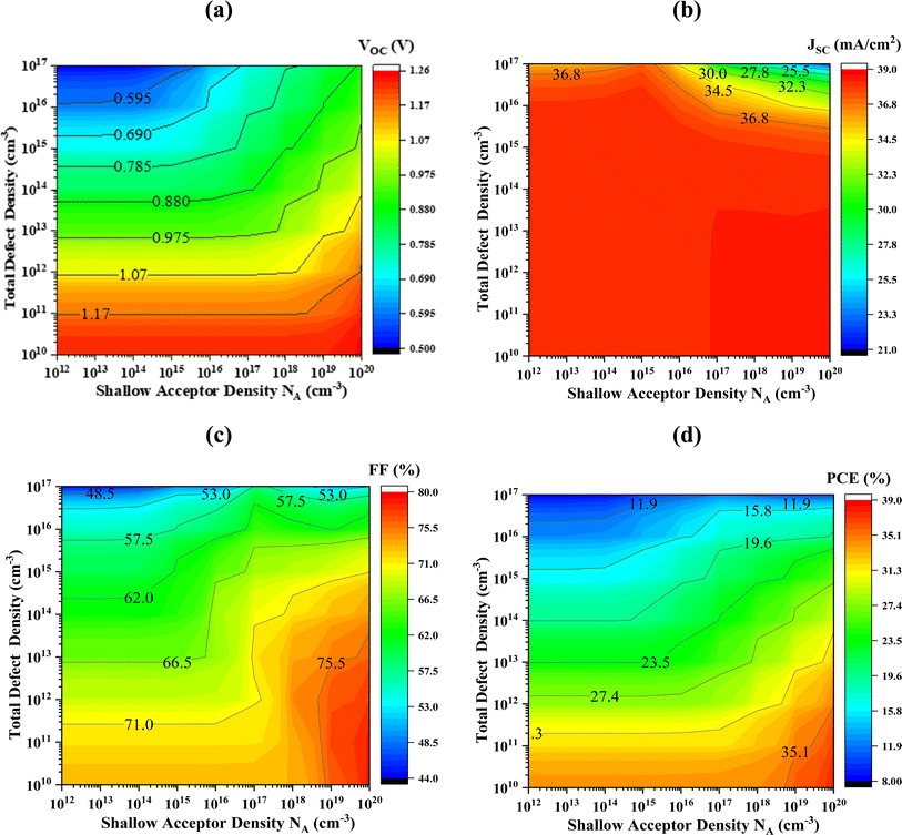 |
| | Fig. 3 Effects of Ba3NCl3 absorber acceptor and bulk defect density variations with HTL CuI on photovoltaic parameters; (a) VOC (b) JSC (c) FF and (d) PCE. | |
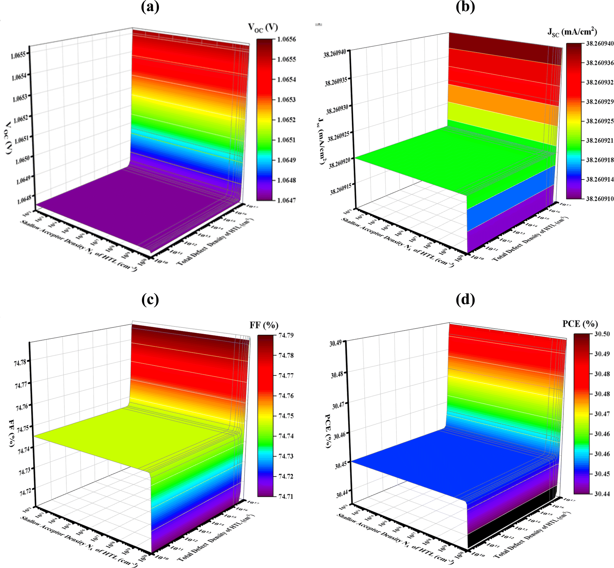
3.3. Impact of HTL CuI layer's bulk defect and acceptor density variation on PV performance
The doping level (NA) of hole transport layers (HTL) can significantly affect the efficiency of photovoltaic devices. A common method for improving conductivity and band alignment between the electrode and absorber layer is doping HTL. Among other things, bandgap, conductivity, and carrier concentration are all impacted by NA in PV devices. Fig. 4 displays the impact of acceptor density NA and bulk defect Nt in HTL CuI on the PV characteristics at 1010 to 1017 cm−3 and 1012 to 1020 cm−3. The PV characteristics with HTL CuI range from 1.0647 to 1.0655 V, 38.260913 to 38.260939 mA cm−2, 74.7104 to 74.7880%, and 30.4357 to 30.4895%, respectively, with the variation of Nt and NA. However, CuI HTL produced the maximum FF of 74.78, JSC of 38.397 mA cm−2, VOC of 1.0655 V, and PCE of 30.48%. To achieve cost-effective manufacturing and high efficiency in practical applications, a Nt of 1012 and a NA level of 1018 cm−3 were selected for more research with HTL CuI. Variations in the defect density (Nt) in PV devices' HTL layer can cause recombination, obstruct charge carrier passage, and jeopardize the stability of the device. Non-uniform fault distribution throughout the HTL can affect optical properties that affect photon absorption and lead to spatial variations in device performance. Ensuring uniformity in the HTL layer and decreasing fault density are the primary ways to optimize PV efficiency and dependability.
 |
| | Fig. 4 Effects of HTL CuI shallow acceptor NA and bulk defect density variations on photovoltaic parameters; (a) VOC (b) JSC (c) FF and (d) PCE. | |
3.4. Analysis of generation-recombination rate and carrier concentration
Fig. 5(a) and (b) display the carrier production and recombination rates for the two scenarios with HTL and without HTL for different locations. An electron creates electron–hole pairs with a hole remaining in the valence band (VB) when it moves from the VB to the conduction band (CB) during carrier creation. This leads to the release of electrons and holes, which increases carrier synthesis in PSCs. Surprisingly, the generation rate with HTL is the lowest at 0.1 μm, whereas the rate without HTL is around 1.03 μm. This difference can be explained by the fact that certain places absorb photons at higher rates than others. Eqn (6) makes it easier to find G(x), and the Nphot (λ, x) SCAPS-1D model uses the incoming photon flux to measure the creation of electron–hole pairs.| | |
G(λ, x) = α(λ, x)·Nphot(λ, x)
| (6) |
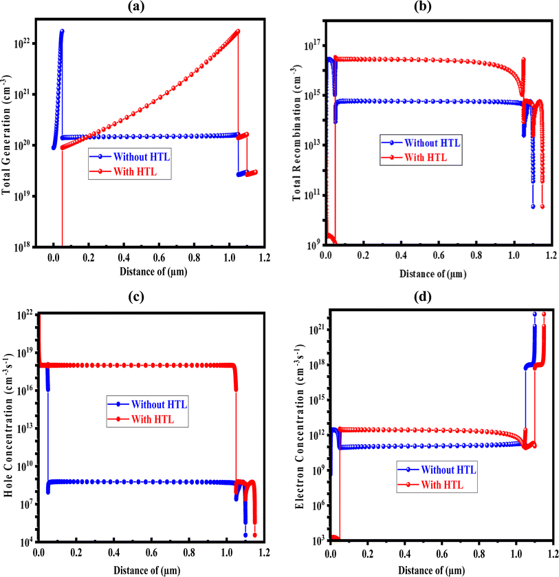 |
| | Fig. 5 (a) The rate of total generation; (b) the rate of recombination; (c) the concentration of hole; and (d) the concentration of electron carrier with and without HTL. | |
Recombination occurs in photovoltaic systems when electrons and holes mix in the conduction band. Recombination rates in precisely designed and optimized PSCs are highly dependent on the density and lifespan of these charge carriers. Moreover, the defect state of every layer affects the recombination process in PSCs. In particular, more electrons from the conduction band pass over the energy barrier and pair with holes in the valence band.
As such, the energy levels related to this transition have an impact on the kinetics of electron–hole recombination. The differences in the thickness of the Ba3NCl3 absorber layer with and without HTL, as well as how they impact the concentrations of electron and hole carriers, are depicted in Fig. 5(c) and (d). The varying absorber concentrations result in different densities of states (DOS) inside the valence bands, which in turn affect the hole concentration in the Ba3NCl3 absorber. It's interesting to note that the former is more prevalent when comparing the concentrations of electrons and holes.47,48 This study shows that employing CuI as HTL in combination with Ba3NCl3 based on barium nitride chloride decreases electron–hole recombination and enhances carrier generation, hence increasing the absorber materials' effectiveness. These advancements may lead to the creation of high-performance PSCs.
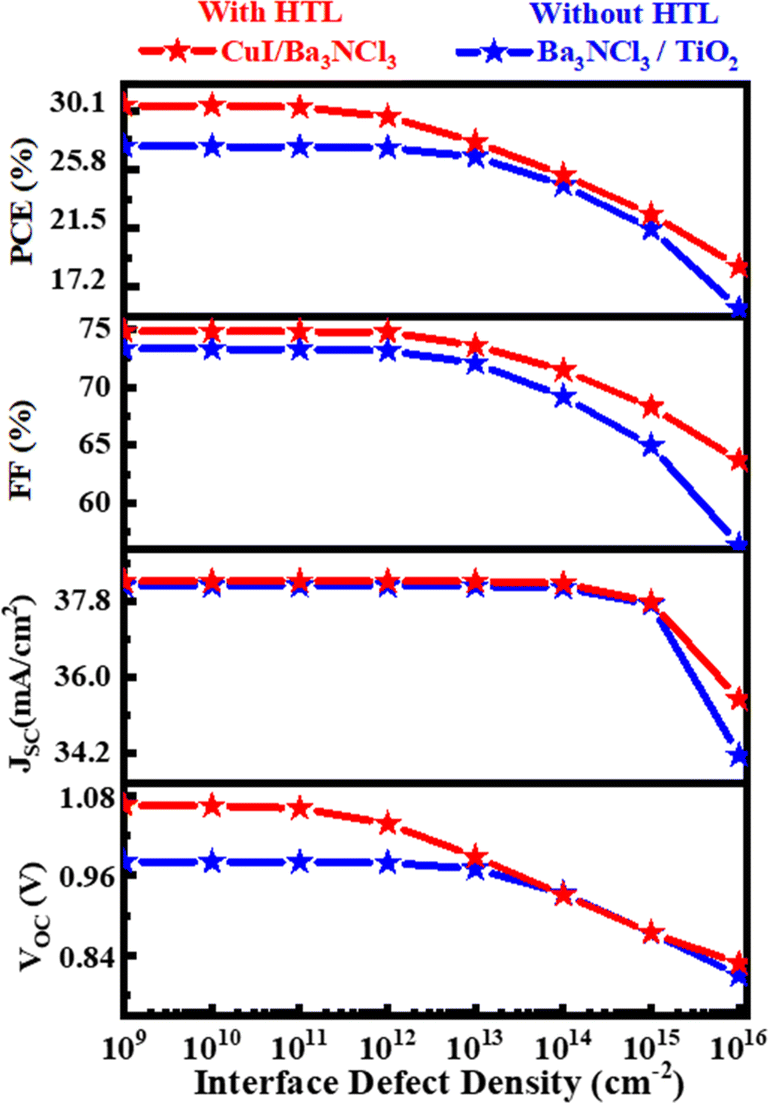
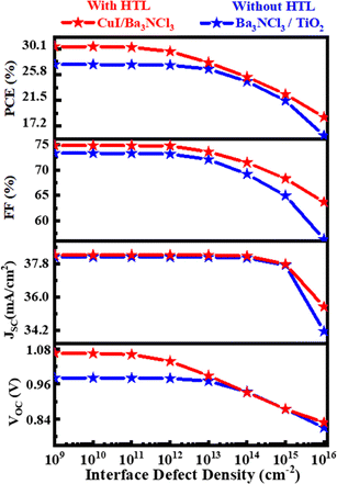
3.5. Analysis of interface defect density on PV performance
The influence of defect interface states on the output parameters is comparable to that of bulk defects. Fig. 6 illustrates how interfacial imperfections at with HTL CuI/Ba3NCl3 and without HTL Ba3NCl3/TiO2 impact the PV characteristics of a newly designed Ba3NCl3-absorber based PSC. Reduced interface defects are essential for optimizing solar cell performance through careful material engineering and interface passivation. Lattice mismatch, thermal expansion differences, chemical reactions, and grain boundaries are common sources of interface defect densities in an Al/FTO/TiO2/Ba3NCl3/CuI/Ni solar cell structure, which impact its efficiency as recombination centers for charge carriers. The analysis and measurement of these defects is done using techniques such as capacitance.
 |
| | Fig. 6 Defect impact on PV parameters at the Ba3NCl3/TiO2 and CuI/Ba3NCl3 interfaces. | |
The concentration of interface faults was varied in this simulated investigation from 109 to 1016 cm−2 while maintaining the same values for all other parameters. With increasing defect density starting at 109 cm−2, PV metrics including PCE, FF, JSC, and VOC are shown in Fig. 6 drastically decline at the with HTL CuI/Ba3NCl3 and without HTL Ba3NCl3/TiO2 interface, going from 30.48 to 18.70% and 27.48 to 15.64%, 74.78 to 63.71% and 73.27 to 56.40%, 38.26 to 35.47 mA cm−2 and 38.25 to 34.24 mA cm−2, and 1.0654 to 0.8278 V and 0.9804 to 0.809 V, respectively. When interface faults exist, series resistance can increase significantly.49,50 However, this resistance has very little effect on JSC, which leads to nearly constant JSC at all three interfaces with varying defect concentrations. The decline in performance is caused by the increased interface carrier recombination rate when defect density rises.51–53 Therefore, it is suggested that interface defects at the Ba3NCl3/TiO2 and CuI/Ba3NCl3 layers have a major role in determining the performance characteristics of PV devices.54,55
3.6. Optimized J–V and QE characteristics
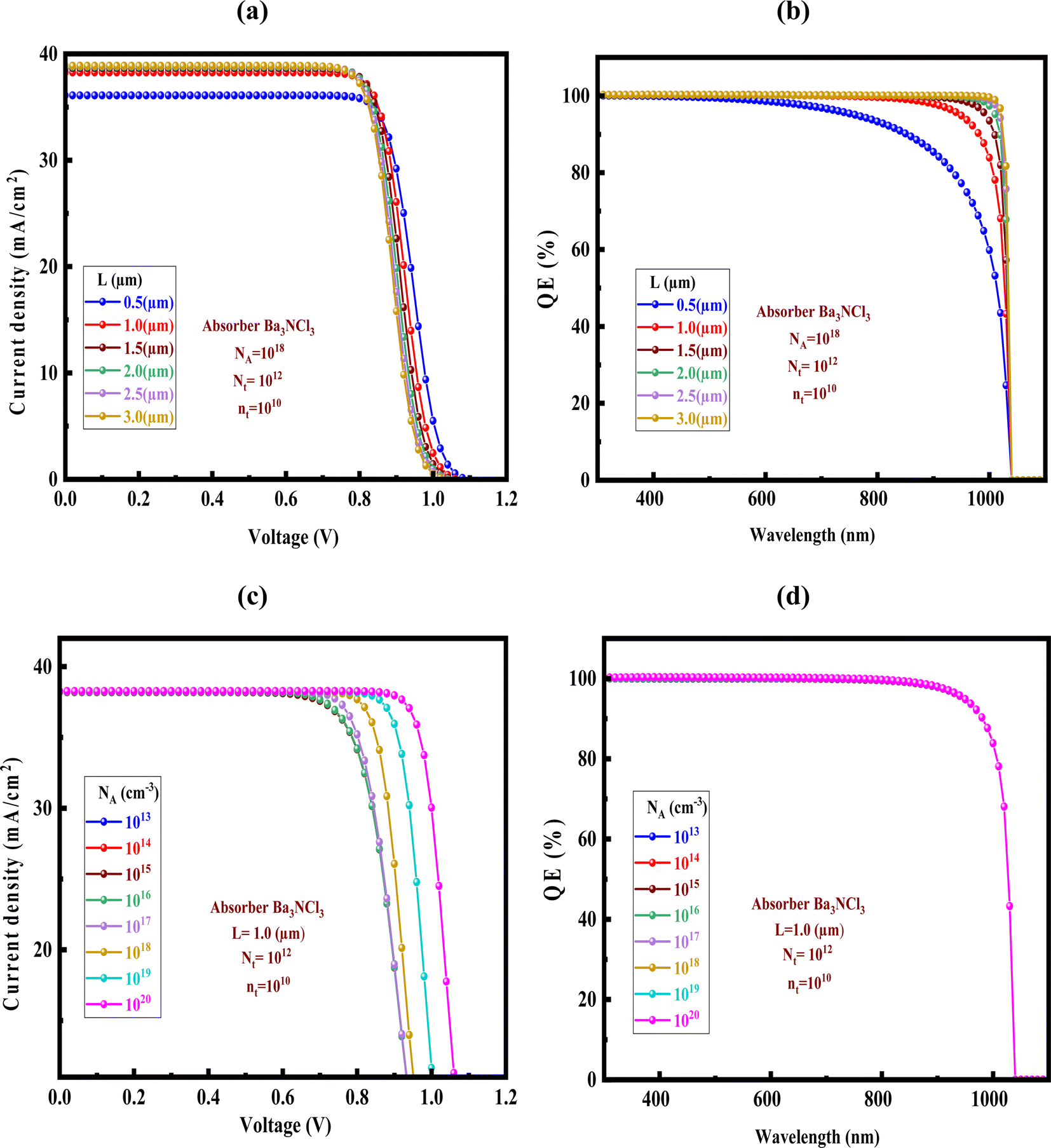
There is a lot of promise for Ba3NCl3 as an absorber layer in solar cells. The quantum efficiency (Q-E) and current–voltage (J–V) properties of the solar cell can be significantly impacted by the thickness of the Ba3NCl3 absorber layer. Increased JSC is frequently the result of increased photocurrent and light absorption from a bigger Ba3NCl3 absorber layer. But a bigger absorber layer might also result in higher recombination losses, which would lower the FF and VOC and eventually lower efficiency. Recent research indicates that the doping level, processing technique, and device design all affect the ideal thickness of the Ba3NCl3 absorber for the fabrication of high-efficiency solar cells.56,57 The J–V characteristics and QE properties are critical indicators of solar cell performance.58 The current density (J) when the voltage (V) across the solar cell is zero is called short-circuit current density (JSC). A higher JSC indicates efficient light absorption and charge carrier collection. VOC is the voltage (V) when the current (J) is zero. VOC is influenced by the material's bandgap and the recombination of charge carriers. QE is the ratio of the number of charge carriers collected by the solar cell to the number of photons incident on the cell at a given wavelength. A higher QE indicates better photon-to-electron conversion efficiency. In some cases, a lighter Ba3NCl3 absorber layer might increase charge carrier collection and decrease recombination losses to reach better efficiency. Because of its impact on photocurrent output and photon absorption efficiency, the thickness of the Ba3NCl3 absorption layer can affect Q-E. Longer wavelength Q-E is greater because more photons can be absorbed by the thicker Ba3NCl3 absorber layer.
On the other hand, if the absorber layer is too thick, light may be absorbed too deeply, which would reduce Q-E and charge carrier collecting efficiency. Fig. 9a and b display the J–V and Q-E characteristics variation with CuI HTL for the variation of absorber thickness. The optimised configurations' PCE reached its highest point at 30.47% CuI HTL, with a VOC 1.0649 V, a FF of 74.78%, and JSC of 38.2609 mA cm−2. The optimised structure's current density zeroes out at 1.06 V with CuI HTL, which is remarkable. It is significant to remember that earlier research has demonstrated a consistent drop in current density as voltage increases, as Fig. 7a and c shows.59,60 The wavelength range covered by the QE profiles from 300–1100 nm. For with HTL, the QE begins at around 100% and gradually decreases to 0% as the wavelength approaches 1040 nm. This drop in QE is consistent with the J–V characteristics results.
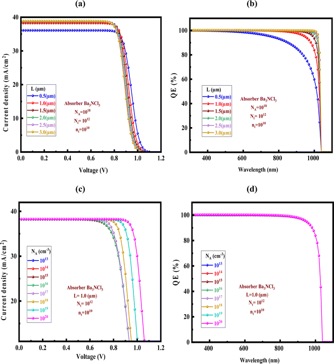 |
| | Fig. 7 Impact of the absorber layer's (a and b) thickness and (c and d) doping concentration on the J–V and QE properties. | |
The effect of the Ba3NCl3 absorber layer doping concentration on the J–V and QE spectra of the corresponding solar cells is seen in Fig. 7c and d, respectively. When the hole doping level surpasses 1018 cm−3, the response of QE significantly decreases in both absorber designs, further revealing the recombination of the photogenerated carrier as predicted by a rise in the recombination of free carrier charges inside the bulk. In the absorber layer, the lower energy (longer wavelength) photons are absorbed significantly. As a result, it was shown that the doping concentration had a significant effect on the total conversion efficiency.61
3.7. Effect of temperature
A comprehensive numerical study that looks at the effects of changing the temperature from 275 to 475 K on PV properties is presented in Fig. 8. Critical metrics such as PCE, VOC, JSC, and FF have consistently been demonstrated to have higher values in produced PSCs with Hole Transport Layer (HTL) than in PSCs without HTL over the complete temperature range. The production and recombination of carriers exhibit a constant rate over the temperature range of 275 to 475 K in this graph. The estimated PCE for the baseline structure without HTL spans from 27.55 to 22.14% for the variation of temperature from 275 K to 475 K, respectively, and ranges from 31.31% to 28.17% with CuI HTL. Temperature can accelerate electron recombination between the valence and conduction bands in some PSC configurations, which can result in an increase in reverse saturation current and a decrease in PCE and VOC.62
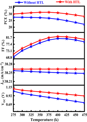 |
| | Fig. 8 Effect of temperature change on PV solar cell. | |
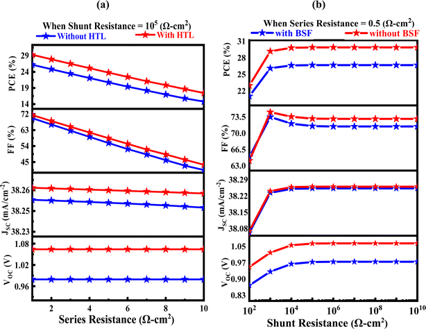
3.8. The effect of the resistances on the PV performance of the proposed solar cell
Using SCAPS-1D software, the impact of the series (Rs) and shunt resistances (Rsh) on the solar device is examined. The circuit terminal resistance, the bulk resistance, and the front and rear metallic contact resistance combine to produce the solar cell's Rs.63 The main result of the series resistance is to reduce the fill factor, which means that a 100% FF is unachievable. To improve efficiency, lower series and greater shunt resistances must be reached. The resistance values have an impact on JSC and VOC as well. The value of Rs is changed using SCAPS-1D to see how it affects the performance of the suggested and conventional solar cells. While the shunt resistance (Rsh) is set at 105 Ω cm2, the value of Rs can vary from 1 to 10 Ω cm2.
As widely noted in the previous literature,64 Fig. 9(a) shows the impact of varying Rs on the proposed cell, including the without HTL and with CuI HTL layer. It is evident from this that raising Rs considerably reduces the solar cell's efficiency. The efficiency decreased from 26.12 to 15.16% and from 29.10 to 18.87% when Rs were changed within the specified range, according to these data. The value of Rsh is now changed from 102 to 1010 Ω cm2 after the series resistance, Rs, is fixed at 0.5 Ω cm2. The results of varying the cell's Rsh value as previously described are shown in Fig. 9(b), which also demonstrates that the efficiency of the suggested solar cell rises as Rsh grows. The efficiency increases with raising the Rsh value of the proposed solar cell, which includes the without HTL and with CuI HTL layer, from 21.55 to 26.80% to 23.35 to 29.79%.
 |
| | Fig. 9 The impact of varying series and shunt (a and b) without HTL and with HTL CuI layers on PV solar cell. | |
4. Conclusion
Using SCAPS-1D, the performance of a novel heterostructure including Al/FTO/TiO2/Ba3NCl3/CuI/Ni in solar devices was examined and assessed. Computational simulations were used to evaluate key parameters of Ba3NCl3-based solar cells with TiO2 serving as the electron transport layer (ETL) and with or without CuI-based hole transport layer (HTL). When comparing this new design to the conventional structure, VOC and PCE showed significant improvements. It was looked at how different gadget features affected solar cell performance. The optimal configurations were determined to be the absorber thickness of 1000 nm and the doping concentration of 1018 cm−3, the HTL CuI thickness of 50 nm, and the TiO2 ETL thickness of 50 nm. There are four different PV values for the proposed Ba3NCl3-based heterojunction with CuI HTL: 30.47% for PCE, 1.0649 V for VOC, 38.2609 mA cm−2 for JSC, and 74.78% for FF. These findings show that the Al/FTO/TiO2/Ba3NCl3/CuI/Ni design has the potential to enable the production of high-efficiency solar cells by the solar cell industry. On the other hand, Ba3NCl3-based photovoltaic cells are limited by assumptions derived from simulations that do not fully capture the complexities of real-world systems. Processing challenges and potential stability and efficiency issues make it challenging to implement recommended solar cell configurations. Obtaining consistent and dependable device performance is also a significant barrier to scaling up production. Ultimately, overcoming these limitations necessitates comprehensive understanding as well as innovative solutions in the domains of material science and device engineering.
Abbreviations
| HTL | Hole transport layer |
| ETL | Electron transport layer |
| PSC | Perovskite solar cell |
| VOC | Open voltage current |
| FF | Fill factor |
| EA | Electron affinity |
| J–V | Current voltage density |
| WF | Work function |
| JSC | Short circuit current density |
| Nt | Defect density |
| μh | Hole mobility |
| χ | Electron affinity |
| Rs | Series resistances |
| SCAPS | Solar cell capacitance simulator |
| SRH | Shockley–Read–Hall |
| EBD | Energy band diagram |
| PV | Photovoltaic |
| FTO | Fluorine-doped tin oxide |
| εr | Dielectric permittivity (relative) |
| PCE | Power conversion efficiency |
| BMC | Back metal contact |
| Q-E | Quantum efficiency |
| ND | Shallow uniform donor density |
| NA | Shallow uniform acceptor density |
| μn | Electron mobility |
| Rsh | Shunt resistances |
Ethical statement
All the authors declare that the manuscript does not have studies on human subjects, human data or tissue, or animals.
Data availability
Data will be made available on reasonable request.
Author contributions
Avijit Ghosh: conceptualization, methodology, software, validation, formal analysis, visualization, investigation, data curation, supervision, writing—original draft, and review and editing. Abdullah Al Hossain Newaz, Abdullah AL Baki, Nasser S. Awwad, and Hala A. Ibrahium: methodology, software, validation, formal analysis, data curation, writing—original draft, and review and editing. Mohammad Shakhawat Hossain, and Md Muminur Rahman Sonic, Md Saiful Islam, and Md Khaledur Rahman: software, validation, formal analysis, writing—original draft, and review and editing.
Conflicts of interest
The authors have no conflicts of interest.
Acknowledgements
The authors extend their appreciation to the Deanship of Research and Graduate Studies at King Khalid University for funding this work under grant number RGP2/148/45.
References
- M. K. Hossain, et al., Harnessing the potential of CsPbBr3-based perovskite solar cells using efficient charge transport materials and global optimization, RSC Adv., 2023, 13(30), 21044–21062, 10.1039/d3ra02485g.
- M. K. Hossain, et al., Numerical Analysis in DFT and SCAPS-1D on the Influence of Different Charge Transport Layers of CsPbBr3 Perovskite Solar Cells, Energy Fuels, 2023, 37(8), 6078–6098, DOI:10.1021/acs.energyfuels.3c00035.
- S. Bhattarai, et al., Perovskite Solar Cells with Dual Light Absorber Layers for Performance Efficiency Exceeding 30%, Energy Fuels, 2023, 37(14), 10631–10641, DOI:10.1021/acs.energyfuels.3c01659.
- M. F. Rahman, et al., An investigation on strain-incited electronic and optical properties of novel inorganic cubic material Sr3AsCl3, J. Solid State Chem., 2023, 328, 124341, DOI:10.1016/j.jssc.2023.124341.
- A. Ghosh, et al., Strain-induced changes in the electronic, optical and mechanical properties of the inorganic cubic halide perovskite Sr3PBr3 with FP-DFT, J. Phys. Chem. Solids, 2024, 191, 112053, DOI:10.1016/j.jpcs.2024.112053.
- A. Ghosh, et al., Structural, electronic and optical characteristics of inorganic cubic perovskite Sr3AsI3, Opt. Continuum, 2023, 2(10), 2144, DOI:10.1364/optcon.495816.
- M. F. Rahman, et al., Unraveling the strain-induced and spin–orbit coupling effect of novel inorganic halide perovskites of Ca3AsI3 using DFT, AIP Adv., 2023, 13(8), 085329, DOI:10.1063/5.0156961.
- M. F. Rahman, et al., The optical and electronic properties of inorganic halide perovskite Sr3NCl3 under applied biaxial strain, J. Mater. Sci., 2023, 58(32), 13100–13117, DOI:10.1007/s10853-023-08825-5.
- A. Ghosh, et al., Inorganic novel cubic halide perovskite Sr3AsI3: strain-activated electronic and optical properties, Heliyon, 2023, 9(8), e19271, DOI:10.1016/j.heliyon.2023.e19271.
- T. Krishnamoorthy, et al., Lead-free germanium iodide perovskite materials for photovoltaic applications, J. Mater. Chem. A, 2015, 3(47), 23829–23832, 10.1039/c5ta05741h.
- M. A. B. Shanto, et al., Investigating how the electronic and optical properties of a novel cubic inorganic halide perovskite, Sr3NI3 are affected by strain, F1000Research, 2023, 12, 1005, DOI:10.12688/f1000research.137044.1.
- A. Kojima, K. Teshima, Y. Shirai and T. Miyasaka, Organometal Halide Perovskites as Visible-Light Sensitizers for Photovoltaic Cells, J. Am. Chem. Soc., 2009, 131(17), 6050–6051, DOI:10.1021/ja809598r.
- P. Ramasamy, D.-H. Lim, B. Kim, S.-H. Lee, M.-S. Lee and J.-S. Lee, All-inorganic cesium lead halide perovskite nanocrystals for photodetector applications, Chem. Commun., 2016, 52(10), 2067–2070, 10.1039/c5cc08643d.
- G. E. Eperon, et al., Inorganic caesium lead iodide perovskite solar cells, J. Mater. Chem. A, 2015, 3(39), 19688–19695, 10.1039/c5ta06398a.
- F. F. Targhi, Y. S. Jalili and F. Kanjouri, MAPbI3 and FAPbI3 perovskites as solar cells: case study on structural, electrical and optical properties, Results Phys., 2018, 10, 616–627, DOI:10.1016/j.rinp.2018.07.007.
- M. K. Hossain, et al., Numerical simulation and optimization of a CsPbI3-based perovskite solar cell to enhance the power conversion efficiency, New J. Chem., 2023, 47(10), 4801–4817, 10.1039/d2nj06206b.
- T. Qiao, D. Parobek, Y. Dong, E. Ha and D. H. Son, Photoinduced Mn doping in cesium lead halide perovskite nanocrystals, Nanoscale, 2019, 11(12), 5247–5253, 10.1039/c8nr10439e.
- M. A. Rahman, et al., Impact of A-Cations Modified on the Structural, Electronic, Optical, Mechanical, and Solar Cell Performance of Inorganic Novel A3NCl3 (A = Ba, Sr, and Ca) Perovskites, Energy Fuels, 2024 DOI:10.1021/acs.energyfuels.4c00525.
- Y. Zheng, et al., Towards 26% efficiency in inverted perovskite solar cells via interfacial flipped band bending and suppressed deep-level traps, Energy Environ. Sci., 2024, 17(3), 1153–1162, 10.1039/d3ee03435f.
- B. Chen, et al., Blade-Coated Perovskites on Textured Silicon for 26%-Efficient Monolithic Perovskite/Silicon Tandem Solar Cells, Joule, 2020, 4(4), 850–864, DOI:10.1016/j.joule.2020.01.008.
- S. Liu, V. P. Biju, Y. Qi, W. Chen and Z. Liu, Recent progress in the development of high-efficiency inverted perovskite solar cells, NPG Asia Mater., 2023, 15(1), 27, DOI:10.1038/s41427-023-00474-z.
- J. Jeong, et al., Pseudo-halide anion engineering for α-FAPbI3 perovskite solar cells, Nature, 2021, 592(7854), 381–385, DOI:10.1038/s41586-021-03406-5.
- Y. Yuan, et al., Photovoltaic Switching Mechanism in Lateral Structure Hybrid Perovskite Solar Cells, Adv. Energy Mater., 2015, 5(15) DOI:10.1002/aenm.201500615.
- F. Hao, C. C. Stoumpos, D. H. Cao, R. P. H. Chang and M. G. Kanatzidis, Lead-free solid-state organic–inorganic halide perovskite solar cells, Nat. Photonics, 2014, 8(6), 489–494, DOI:10.1038/nphoton.2014.82.
- G. S. Lotey, et al., Boosting efficiency and stability of perovskite solar cells via integrating engineered Li/Na-ferrite-based inorganic charge transport layers: a combined experimental and theoretical study, J. Nanopart. Res., 2023, 25(9), 179, DOI:10.1007/s11051-023-05827-x.
- F. Paquin, J. Rivnay, A. Salleo, N. Stingelin and C. Silva-Acuña, Multi-phase microstructures drive exciton dissociation in neat semicrystalline polymeric semiconductors, J. Mater. Chem. C, 2015, 3(41), 10715–10722, 10.1039/c5tc02043c.
- G. S. Lotey, et al., Potential of low-cost inorganic CaFeO3 as transporting material for efficient perovskite solar cells, Mater. Today Commun., 2023, 35, 105956, DOI:10.1016/j.mtcomm.2023.105956.
- A. K. Sharma and D. K. Kaushik, Numerical simulation of MASnI3/CuI heterojunction based perovskite solar cell, J. Phys.: Conf. Ser., 2022, 2267(1), 012148, DOI:10.1088/1742-6596/2267/1/012148.
- A. Ghosh, et al., Improving the power conversion efficiency of RbPbBr3 absorber based solar cells through the variation of efficient hole transport layers, J. Phys. Chem. Solids, 2024, 193, 112179, DOI:10.1016/j.jpcs.2024.112179.
- A. Ait Abdelkadir, E. Oublal, M. Sahal and A. Gibaud, Numerical simulation and optimization of n-Al-ZnO/n-CdS/p-CZTSe/p-NiO (HTL)/Mo solar cell system using SCAPS-1D, Results Opt., 2022, 8, 100257, DOI:10.1016/j.rio.2022.100257.
- M. S. Chowdhury, et al., Effect of deep-level defect density of the absorber layer and n/i interface in perovskite solar cells by SCAPS-1D, Results Phys., 2020, 16, 102839, DOI:10.1016/j.rinp.2019.102839.
- M. F. Hossain, et al., Design and simulation numerically with performance enhancement of extremely efficient Sb2Se3-based solar cell with V2O5 as the hole transport layer, using SCAPS-1D simulation program, Opt. Commun., 2024, 559, 130410, DOI:10.1016/j.optcom.2024.130410.
- Y. H. Khattak, F. Baig, A. Shuja, S. Beg and B. M. Soucase, Numerical analysis guidelines for the design of efficient novel nip structures for perovskite solar cell, Sol. Energy, 2020, 207, 579–591, DOI:10.1016/j.solener.2020.07.012.
- A. Ghosh, et al., Enhancing solar cell efficiency beyond 27% through the implementation of an efficient charge transport layer utilizing an innovative inorganic perovskite Sr3PI3, J. Phys. Chem. Solids, 2024, 190, 112029, DOI:10.1016/j.jpcs.2024.112029.
- N. Jahan, et al., A comparative study of CuO based solar cell with ZnTe HTL and SnS2 ETL using SCAPS 1D simulation, J. Opt., 2024 DOI:10.1007/s12596-024-01800-6.
- S. R. Al Ahmed, A. Sunny and S. Rahman, Performance enhancement of Sb2Se3 solar cell using a back surface field layer: a numerical simulation approach, Sol. Energy Mater. Sol. Cells, 2021, 221, 110919, DOI:10.1016/j.solmat.2020.110919.
- M. S. Islam, et al., An in-depth analysis of how strain impacts the electronic, optical, and output performance of the Ca3NI3 novel inorganic halide perovskite, J. Phys. Chem. Solids, 2024, 185, 111791, DOI:10.1016/j.jpcs.2023.111791.
- M. S. Reza, et al., Boosting efficiency above 28% using effective charge transport layer with Sr3SbI3 based novel inorganic perovskite, RSC Adv., 2023, 13(45), 31330–31345, 10.1039/d3ra06137j.
- M. F. Rahman, et al., Exploring the impact of strain on the electronic and optical properties of inorganic novel cubic perovskite Sr3PI3, Phys. Scr., 2023, 98(11), 115105, DOI:10.1088/1402-4896/acfce9.
- M. S. Reza, et al., Design and Optimization of High-Performance Novel RbPbBr3-Based Solar Cells with Wide-Band-Gap S-Chalcogenide Electron Transport Layers (ETLs), ACS Omega, 2024, 9(18), 19824–19836, DOI:10.1021/acsomega.3c08285.
- M. H. Mohammadi, D. Fathi and M. Eskandari, Light trapping in perovskite solar cells with plasmonic core/shell nanorod array: a numerical study, Energy Rep., 2021, 7, 1404–1415, DOI:10.1016/j.egyr.2021.02.071.
- N. Solhtalab, M. H. Mohammadi, M. Eskandari and D. Fathi, Efficiency improvement of half-tandem CIGS/perovskite solar cell by designing nano-prism nanostructure as the controllable light trapping, Energy Rep., 2022, 8, 1298–1308, DOI:10.1016/j.egyr.2021.12.038.
- M. Samiul Islam, et al., Defect Study and Modelling of SnX3-Based Perovskite Solar Cells with SCAPS-1D, Nanomaterials, 2021, 11(5), 1218, DOI:10.3390/nano11051218.
- U. Mandadapu, Simulation and Analysis of Lead based Perovskite Solar Cell using SCAPS-1D, Indian J. Sci. Technol., 2017, 10(1), 1–8, DOI:10.17485/ijst/2017/v11i10/110721.
- Ferdiansjah, Faridah and K. Tirtakusuma Mularso, Analysis of Back Surface Field (BSF) Performance in P-Type And N-Type Monocrystalline Silicon Wafer, E3S Web Conf., 2018, 43, 01006, DOI:10.1051/e3sconf/20184301006.
- G. K. Gupta, A. Garg and A. Dixit, Electrical and impedance spectroscopy analysis of sol-gel derived spin coated Cu2ZnSnS4 solar cell, J. Appl. Phys., 2018, 123(1) DOI:10.1063/1.5002619.
- Y. Zhou and A. Gray-Weale, A numerical model for charge transport and energy conversion of perovskite solar cells, Phys. Chem. Chem. Phys., 2016, 18(6), 4476–4486, 10.1039/c5cp05371d.
- O. Ahmad, A. Rashid, M. W. Ahmed, M. F. Nasir and I. Qasim, Performance evaluation of Au/p-CdTe/Cs2TiI6/n-TiO2/ITO solar cell using SCAPS-1D, Opt. Mater., 2021, 117, 111105, DOI:10.1016/j.optmat.2021.111105.
- Z. Gu, et al., Novel planar heterostructure perovskite solar cells with CdS nanorods array as electron transport layer, Sol. Energy Mater. Sol. Cells, 2015, 140, 396–404, DOI:10.1016/j.solmat.2015.04.015.
- M. S. Reza, et al., New highly efficient perovskite solar cell with power conversion efficiency of 31% based on Ca3NI3 and an effective charge transport layer, Opt. Commun., 2024, 561, 130511, DOI:10.1016/j.optcom.2024.130511.
- M. Burgelman, J. Verschraegen, S. Degrave and P. Nollet, Modeling thin-film PV devices, Prog. Photovoltaics Res. Appl., 2004, 12(23), 143–153, DOI:10.1002/pip.524.
- L. Vinet and A. Zhedanov, A ‘missing’ family of classical orthogonal polynomials, J. Phys. A: Math. Theor., 2011, 44(8), 085201, DOI:10.1088/1751-8113/44/8/085201.
- C. Chen, et al., Characterization of basic physical properties of Sb2Se3 and its relevance for photovoltaics, Front. Optoelectron., 2017, 10(1), 18–30, DOI:10.1007/s12200-017-0702-z.
- H. Zhang, S. Cheng, J. Yu, H. Zhou and H. Jia, Prospects of Zn(O,S) as an alternative buffer layer for Cu2ZnSnS4 thin-film solar cells from numerical simulation, Micro Nano Lett., 2016, 11(7), 386–390, DOI:10.1049/mnl.2016.0130.
- Y. H. Khattak, F. Baig, H. Toura, S. Beg and B. M. Soucase, Efficiency enhancement of Cu2BaSnS4 experimental thin-film solar cell by device modeling, J. Mater. Sci., 2019, 54(24), 14787–14796, DOI:10.1007/s10853-019-03942-6.
- P. Zhan, J. Chen and L. Chen, Influence of SnO2, ZnO and TiO2 layer on the performance of CIGS and CdTe solar cells, IOP Conf. Ser. Earth Environ. Sci., 2021, 781(4), 042069, DOI:10.1088/1755-1315/781/4/042069.
- A. Ghosh, et al., Investigating of novel inorganic cubic perovskites of A3BX3 (A = Ca, Sr, B
![[double bond, length as m-dash]](https://www.rsc.org/images/entities/char_e001.gif) P, As, X = I, Br) and their photovoltaic performance with efficiency over 28%, J. Alloys Compd., 2024, 986, 174097, DOI:10.1016/j.jallcom.2024.174097.
P, As, X = I, Br) and their photovoltaic performance with efficiency over 28%, J. Alloys Compd., 2024, 986, 174097, DOI:10.1016/j.jallcom.2024.174097. - M. F. I. Buian, et al., A novel investigation into strain-induced changes in the physical properties and solar cell performances of lead-free Ca3NCl3 perovskite, Mater. Sci. Semicond. Process., 2024, 180, 108580, DOI:10.1016/j.mssp.2024.108580.
- M. S. Islam, et al., Investigation strain effects on the electronic, optical, and output performance of the novel inorganic halide perovskite Sr3SbI3 solar cell, Chin. J. Phys., 2024, 88, 270–286, DOI:10.1016/j.cjph.2024.01.011.
- P. Khan, T. Mahmood, K. Ayub, S. Tabassum and M. Amjad Gilani, Turning diamondoids into nonlinear optical materials by alkali metal substitution: a DFT investigation, Opt. Laser Technol., 2021, 142, 107231, DOI:10.1016/j.optlastec.2021.107231.
- M. F. Rahman, et al., Concurrent investigation of antimony chalcogenide (Sb2Se3 and Sb2S3)-based solar cells with a potential WS2 electron transport layer, Heliyon, 2022, 8(12), e12034, DOI:10.1016/j.heliyon.2022.e12034.
- F. Behrouznejad, S. Shahbazi, N. Taghavinia, H.-P. Wu and E. Wei-Guang Diau, A study on utilizing different metals as the back contact of CH3NH3PbI3 perovskite solar cells, J. Mater. Chem. A, 2016, 4(35), 13488–13498, 10.1039/c6ta05938d.
- H. Heriche, Z. Rouabah and N. Bouarissa, New ultra thin CIGS structure solar cells using SCAPS simulation program, Int. J. Hydrogen Energy, 2017, 42(15), 9524–9532, DOI:10.1016/j.ijhydene.2017.02.099.
- A. Sylla, S. Touré and J.-P. Vilcot, Numerical Modeling and Simulation of CIGS-Based Solar Cells with ZnS Buffer Layer, Open J. Model. Simul., 2017, 5(4), 218–231, DOI:10.4236/ojmsi.2017.54016.
|
| This journal is © The Royal Society of Chemistry 2024 |
Click here to see how this site uses Cookies. View our privacy policy here. 
 Open Access Article
 This Open Access Article is licensed under a Creative Commons Attribution-Non Commercial 3.0 Unported Licence
 *a,
Abdullah Al Hossain Newazb,
Abdullah Al Bakic,
Nasser S. Awwadd,
Hala A. Ibrahiume,
Mohammad Shakhawat Hossainc,
Md Muminur Rahman Sonicc,
Md Saiful Islamc and
Md Khaledur Rahmanc
*a,
Abdullah Al Hossain Newazb,
Abdullah Al Bakic,
Nasser S. Awwadd,
Hala A. Ibrahiume,
Mohammad Shakhawat Hossainc,
Md Muminur Rahman Sonicc,
Md Saiful Islamc and
Md Khaledur Rahmanc