
 Open Access Article
 This Open Access Article is licensed under a Creative Commons Attribution-Non Commercial 3.0 Unported Licence
Constructing drain surrounded double gate structure in AlGaN/GaN HEMT for boosting breakdown voltage
Zehui Peng ,
Huangbai Liu,
Hao Yu,
Lei Li* and
Kuan-Chang Chang*
,
Huangbai Liu,
Hao Yu,
Lei Li* and
Kuan-Chang Chang*
School of Electronic and Computer Engineering, Peking University, Shenzhen 518055, China. E-mail: kcchang@pkusz.edu.cn
First published on 15th July 2024
Abstract
AlGaN/GaN high electron mobility transistors (HEMTs) play an important role in the field of high-voltage and high-frequency power devices. However, the current collapse effect of the HEMTs under high voltage greatly limits the development of AlGaN/GaN HEMTs. In this work, a breakdown performance enhanced drain surrounded double gate (DSDG) AlGaN/GaN HEMT is investigated. This structure has two separate gates located on the right and the left of the drain. The optimized off-state characteristics are analyzed by the Sentaurus TCAD simulation tool. The additional gate contributes to restraining the movement of electrons injected by the source therefore reducing the source-to-drain punch-through current. Moreover, the energy band pulled up by the relatively low voltage of the right gate helps to alleviate the drain induced barrier lower (DIBL) effect. As a result, DSDG-HEMT could postpone the breakdown by approximately 100 V through suppressing buffer leakage.
1. Introduction
Gallium nitride (GaN), as the most promising third-generation semiconductor material, has extensive applications in high-voltage fields such as electric vehicles, photovoltaic inverters, and power grid equipment.1–3 AlGaN/GaN high electron mobility transistors (HEMTs) based on GaN materials emerge as promising candidates for high-power applications due to outstanding physical properties.4 However, the non-ideal off-state performance limits the HEMT device's further development.5 Although the breakdown voltage (BV) of GaN has significantly surpassed traditional silicon-based devices, existing BV levels still fall short of requirements in some high-voltage applications, such as high-voltage power transmission systems or extremely high-power scenarios.6–8 Besides, the overall mechanisms of breakdown induced by buffer leakage remain ambiguous.9,10 Therefore, insufficient BV has become a key problem limiting the wide application of GaN HEMTs, and effective methods are urgently needed to eliminate the negative impact of buffer leakage on BV. Increasing the BV of GaN HEMTs enables devices to remain stable under adverse conditions, improving overall system reliability, tolerating higher transient voltages, and enhancing overload and surge capability.11,12 GaN HEMTs with high BV can also operate at higher voltages, increasing power density, reducing system size and weight, and expanding their applications in high-voltage scenarios.However, the breakdown mechanism of GaN HEMTs is often the result of multiple interacting factors, making the overall breakdown process more complex.5,6 In the design and manufacturing process, various factors should be considered comprehensively, and the leakage current of the buffer layer should be reduced by optimizing the epitaxial growth, device structure design, and process flow to prevent breakdown. Among these factors, buffer layer leakage currents pose a significant issue impacting device performance.10 Under high electric fields, electrons in the buffer layer may leak through quantum tunneling or Fowler–Nordheim tunneling, causing breakdown.13 In regions with high electric fields in the buffer layer, impact ionization between electrons and holes may trigger avalanche breakdown.14 Thus, numerous studies have proposed various methods to improve GaN HEMT BV across different dimensions, including materials, processes, and device structures.1,9 These methods include improving material quality, reducing defects and impurities to decrease leakage currents, using higher-quality epitaxial materials to minimize the effects of trap states and other material defects on the electric field, and optimizing device structure designs, such as employing field plate structures or stepped structures.15–17 In previous research, the adoption of a two-level wrap-around gate design (where the gate encircles the drain) could reduce manufacturing costs by eliminating the mesa isolation step.18 Based on this design, a drain-surrounding structure is proposed by Hui Sun et al. to reduce leakage of mesa and isolation region.19 Among these strategies, the field-plate (FP) structure significantly enhances GaN HEMT BV by introducing metal plates to the gate, drain, or source electrodes, improving the electric field distribution, reducing peak electric fields, and ensuring a more uniform field distribution, thereby improving BV and device stability.20–23
In addition, in the field of chip manufacturing, the cost of tape-out is extremely high. Therefore, it is necessary to combine device modeling and theoretical calculation24 to observe whether the device function is consistent with the design expectation in advance when designing new devices. Enlightened by FP structure, this study proposes a GaN HEMT device featuring a drain surrounded double gate structure that incorporates a double gate design around the drain to control the electric field distribution, reducing peak electric fields, and thus enhancing BV. Each side of the drain has a gate, referred to as the inner gate and outer gate. The inner gate forms the primary switching region with the drain, controlling the electric field in the drain region to reduce the peak electric field between the gate and the drain. The outer gate surrounds the drain area, further reducing peak electric fields and minimizing field concentration. Simulation results indicate that this double gate structure effectively alleviates field concentration effects, contributes to suppressing buffer leakage effectively and the BV is improved by approximately 100 V. With an improved electric field distribution, the on-resistance is reduced, and the conduction performance is enhanced. Although the dual gate structure has higher requirements for the process than the simple FP structure, the drain-surrounded double gate AlGaN/GaN high electron mobility transistor (DSDG-HEMT) can control the electric field distribution more accurately and provide higher electric field control ability through the voltage regulation of the dual gate, which is more suitable for high-voltage and high-frequency applications that require more accurate electric field control and lower on-resistance. In summary, the strategy of improving the BV of GaN HEMT devices by designing the double gate structure proposed in this research is of great significance for expanding its use in high-power and high-voltage applications and can improve system efficiency and reliability. DSDG-HEMT has unique advantages in specific applications due to more accurate electric field control, such as higher performance potential in high-frequency and high-voltage applications.
2. Results and discussion
The cross-sectional schematic of the DSDG-HEMT is shown in Fig. 1a. The epitaxial structure consists of a 2 μm thick Al0.05Ga0.95N bottom barrier layer, a 10 nm thick GaN channel layer, a 15 nm thick Al0.23Ga0.77N barrier layer, a 110 nm thick P-doped p-GaN layer and a 200 nm thick Si3N4 passivation layer. The source–gate length LGS and the drain–gate length LGD are 1 μm and 10 μm respectively. The second gate on the right of the drain is placed 1 μm away from the drain. The length of the first gate LFG and the second gate LSG are 1 μm and 0.5 μm respectively. A conventional gate structure HEMT (CG-HEMT) with identical design and dimension is also simulated for comparison.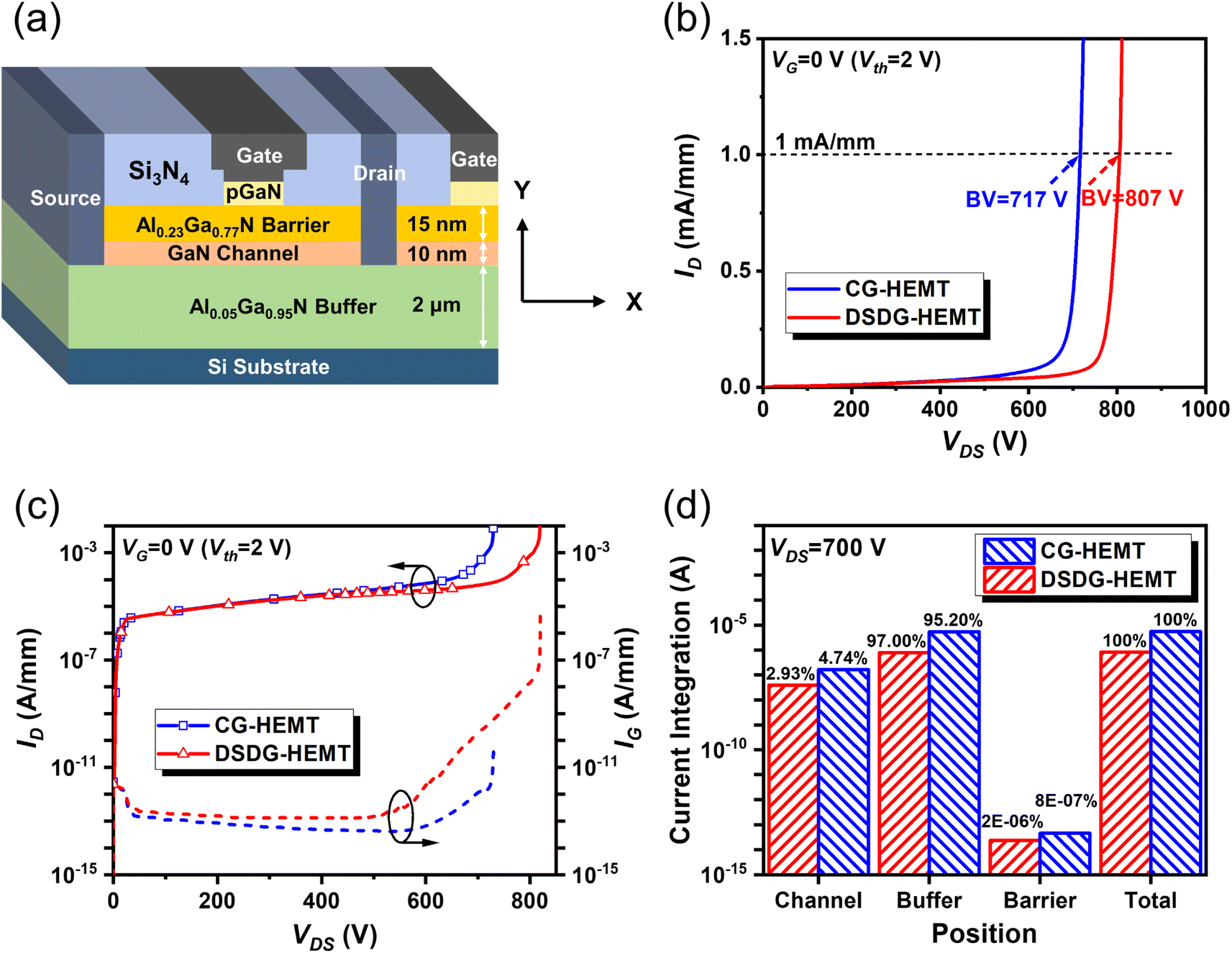 | ||
| Fig. 1 (a) Device schematics of DSDG-HEMT; breakdown and off-state leakage performance of DSDG-HEMT and CG-HEMT. (b) Breakdown performance, (c) drain and gate off-state leakage; (d) leakage integration, and the percentage taken of each layer of DSDG-HEMT and CG-HEMT. | ||
The breakdown characteristics of DSDG-HEMT and CG-HEMT are shown in Fig. 1b. The BV is extracted where the off-state drain current reaches 1 mA mm−1. The DSDG-HEMT delivers a nearly 100 V higher BV than that of CG-HEMT (807 V and 717 V respectively). To investigate the reason for improved BV, the leakage currents from drain and gate contacts are monitored during the off-state I–V measurement. As illustrated in Fig. 1c, the overlarge drain leakage is the main cause of breakdown for both devices. DSDG-HEMT effectively suppresses the drain leakage under relatively large VDS, resulting in higher BV. Different from the drain current, the gate current of DSDG-HEMT is higher than CG-HEMT and experiences a sudden increase after VDS reaches 500 V, which is attributed to the double gate structure extending the area where leakage may occur. To solve this problem, the combination of Si3N4 and high-k materials such as HfO2 and Ta2O5 can be considered as the gate dielectric material to reduce the gate leakage in the future.
The epitaxial layer current integration of two devices at VDS = 700 V is carried out through TCAD tools. As shown in Fig. 1d, the columns represent the leakage of each layer in the log scale. The numbers above columns mean the leakage percentage this layer is taken. The total leakage of DSDG-HEMT is only 15% of CG-HEMT leakage (5.39 × 10⁻⁶ A and 7.88 × 10⁻⁷ A respectively). Besides, DSDG-HEMT has a lower leakage current in each epitaxial layer. It is also found that the main proportion of leakage comes from the buffer layer in both devices. Therefore, the proposed drain-surrounded structure exhibits larger BV through effectively suppressed buffer leakage.
As shown in Fig. 2, both devices have a distinct electron movement path (red arrow) that starts from the source and points to the drain in the buffer layer, representing a source-to-drain punch-through current. For CG-HEMT, this current extends closer to the drain with a higher current density as the drain voltage increases, and the movement path is more dispersed. In contrast, DSDG-HEMT restricts the punch-through currents and terminates its extension far from the drain area at VDS = 600 V. Furthermore, the buffer layer near the drain area of DSDG-HEMT exhibits much lower leakage compared to CG-HEMT.
 | ||
| Fig. 2 Current distribution of CG-HEMT (a) at VDS = 200 V (b) at VDS = 600 V and DSDG-HEMT (c) at VDS = 200 V (d) at VDS = 600 V. | ||
To further compare the leakage distribution, the lateral buffer current density was extracted in the location of Y = 1.5 μm at VDS = 200 V, 500 V, and 700 V. Similarly, the vertical leakage is extracted in the location of the drain electrode (X = 13.0, 13.1, 13.2, 13.3 μm respectively) at VDS = 700 V. It can be observed from Fig. 3 that the current distribution along X-axis of two devices shows similar trend. Furthermore, these two devices deliver almost the same current density when VDS = 200 V. When VDS = 500 V, the buffer current density of DSDG-HEMT is significantly lower than that of CG-HEMT, but the two curves still partially overlap. However, the buffer current density of DSDG-HEMT is significantly lower than CG-HEMT at VDS = 700 V, and the two curves are completely separated. For vertical current density distribution displayed in Fig. 4, the leakage increases first and then decreases along the Y-axis. DSDG-HEMT delivers lower current density in all four curves and the leakage decreases to a negligible value in a shallower position of the buffer layer. These phenomena suggest that DSDG-HEMT not only reduces buffer punch-through currents but also restrains the leakage near the drain contact.
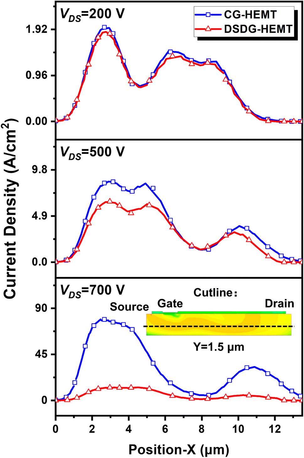 | ||
| Fig. 3 Current density along the X-axis in the buffer layer (Y = 1.5 μm). | ||
 | ||
| Fig. 4 Current density along the Y-axis in the area of the drain electrode. | ||
Further analysis is required to reveal the internal mechanisms of reduced buffer leakage. Fig. 5 shows the electric field (blue arrows) in the area near the drain electrode when VDS = 700 V. It is widely accepted that the drain-to-source electric field accelerates the source injected electrons and thus forms a punch-through current. The presence of the second gate introduces an opposite electric field direction from the drain to the right, which contributes to weakening the influence of the premier direction electric field on electron acceleration. The suppressed acceleration also leads to less severe collision and further restrains the extension of punch-through currents. In addition, the DSDG-HEMT has an additional electron movement path from the second gate to the drain due to the opposite electric field. This phenomenon is consistence with the higher gate leakage as presented in Fig. 1c.
 | ||
| Fig. 5 The influence the second gate has on buffer leakage current. | ||
The reduced buffer leakage is also related to the mitigated drain induced barrier lower (DIBL) effect. High drain voltage will lead to a significantly lower barrier between two-dimensional electron gas and the buffer layer. Consequently, the source electrode can introduce a large number of electrons to the buffer layer through direct injection or defects-assisted tunneling. Fig. 6 shows the lateral conduction band energy level of the buffer layer in the position of Y = 1.5 μm under different drain voltages. The conduction band energy becomes much lower with the increase of VDS. Different from the single direction decrease from source to drain in CG-HEMT, the band energy of DSDG-HEMT shows an increase near the drain. This is due to the pull-up effect of the low voltage from the second gate. The increased band energy helps to suppress related electron movement from source to buffer and, thereby, decreasing the buffer leakage.
 | ||
| Fig. 6 Conduction band energy distribution of DSDG-HEMT and CG-HEMT along the X-axis (Y = 1.5 μm) under different drain voltage. | ||
3. Conclusions
The drain-surrounded double gate HEMT with improved breakdown characteristics is investigated. The increase in BV is attributed to reduced buffer leakage. The second gate located on the right of the drain introduces an opposite-direction electric field. This electric field helps to restrain the acceleration of source-injected electrons, which suppresses the source-to-drain punch-through currents. On the other hand, the lower voltage of the second gate helps to lift the energy band, leading to a weakened DIBL effect. These two mechanisms result in lower buffer leakage, thus postponing breakdown by about 100 V. In the future, the combination of Si3N4 and high-k materials such as HfO2 and Ta2O5 can be considered as the gate dielectric material to reduce the gate leakage to further improve the current DSDG-HEMT.4. Experimental section
The simulation of the DSDG-HEMT and CG-HEMT devices is implemented by the Sentaurus TCAD simulator. Some modified physical models including Shockley–Read–Hall, Fermi statistics, thermionic, piezoelectric polarization, and electron avalanche are used to promote the accuracy.Data availability
The authors confirm that the data supporting the findings of this study are available within the article.Author contributions
Zehui Peng: investigation, formal analysis, visualization, writing original draft, writing – review & editing. Huangbai Liu: data curation, validation, writing – review & editing. Hao Yu: visualization. Lei Li: resources, project administration. Kuan-Chang Chang: conceptualization, methodology, writing – review & editing, funding acquisition.Conflicts of interest
There are no conflicts to declare.Acknowledgements
This study was supported by National Natural Science Foundation of China (No: 62204007, 62074007), Guangdong Provincial Natural Science Foundation (Youth Promotion Project) (No. 2024A1515030044), and Shenzhen Municipal Scientific Program (No. JCYJ20220531093210023, RCYX20231211090332037).References
- N.-Q. Zhang, S. Keller, G. Parish, S. Heikman, S. DenBaars and U. Mishra, High breakdown GaN HEMT with overlapping gate structure, IEEE Electron Device Lett., 2000, 21, 421–423 Search PubMed.
- Y.-F. Wu, D. Kapolnek, J. P. Ibbetson, P. Parikh, B. P. Keller and U. K. Mishra, Very-high power density AlGaN/GaN HEMTs, IEEE Trans. Electron Devices, 2001, 48, 586–590 CrossRef CAS.
- X. Huang, Z. Liu, Q. Li and F. C. Lee, Evaluation and application of 600 V GaN HEMT in cascode structure, IEEE Trans. Power Electron., 2013, 29, 2453–2461 Search PubMed.
- S. Fujita, Wide-bandgap semiconductor materials: For their full bloom, Jpn. J. Appl. Phys., 2015, 54, 030101 CrossRef CAS.
- G. Meneghesso, M. Meneghini and E. Zanoni, Breakdown mechanisms in AlGaN/GaN HEMTs: an overview, Jpn. J. Appl. Phys., 2014, 53, 100211 CrossRef.
- M. A. Khan, M. S. Shur, Q. Chen and J. Kuznia, Current/voltage characteristic collapse in AlGaN/GaN heterostructure insulated gate field effect transistors at high drain bias, Electron. Lett., 1994, 30, 2175–2176 CrossRef CAS.
- G. Koley, V. Tilak, L. F. Eastman and M. G. Spencer, Slow transients observed in AlGaN/GaN HFETs: effects of SiN/sub x/passivation and UV illumination, IEEE Trans. Electron. Dev., 2003, 50, 886–893 CrossRef CAS.
- I. Daumiller, D. Theron, C. Gaquière, A. Vescan, R. Dietrich, A. Wieszt, H. Leier, R. Vetury, U. Mishra and I. Smorchkova, Current instabilities in GaN-based devices, IEEE Electron Device Lett., 2001, 22, 62–64 CAS.
- S. Karmalkar and U. K. Mishra, Enhancement of breakdown voltage in AlGaN/GaN high electron mobility transistors using a field plate, IEEE Trans. Electron. Dev., 2001, 48, 1515–1521 CrossRef CAS.
- Y. Dora, A. Chakraborty, S. Heikman, L. McCarthy, S. Keller, S. DenBaars and U. Mishra, Effect of ohmic contacts on buffer leakage of GaN transistors, IEEE Electron Device Lett., 2006, 27, 529–531 CAS.
- J. He, W. C. Cheng, Q. Wang, K. Cheng, H. Yu and Y. Chai, Recent advances in GaN-based power HEMT devices, Adv. Electron. Mater., 2021, 7, 2001045 CrossRef CAS.
- J. Cui, M. Wang, Y. Wu, J. Yang, H. Yang, J. Yu, T. Li, X. Yang, X. Liu and K. Cheng, Demonstration of 1200-V E-mode GaN-on-sapphire power transistor with low dynamic ON-resistance based on active passivation technique, IEEE Electron Device Lett., 2023, 45(2), 220–223 Search PubMed.
- I. Jabbari, M. Baira, H. Maaref and R. Mghaieth, Evidence of Poole-frenkel and Fowler-Nordheim tunneling transport mechanisms in leakage current of (Pd/Au)/Al0.22Ga0.78N/GaN heterostructures, Solid State Commun., 2020, 314, 113920 CrossRef.
- V. Joshi, S. P. Tiwari and M. Shrivastava, Part I: Physical insight into carbon-doping-induced delayed avalanche action in GaN buffer in AlGaN/GaN HEMTs, IEEE Trans. Electron. Dev., 2018, 66, 561–569 Search PubMed.
- S. Karmalkar and U. K. Mishra, Very high voltage AlGaN/GaN high electron mobility transistors using a field plate deposited on a stepped insulator, Solid-State Electron., 2001, 45, 1645–1652 CrossRef CAS.
- W. Saito, Y. Kakiuchi, T. Nitta, Y. Saito, T. Noda, H. Fujimoto, A. Yoshioka, T. Ohno and M. Yamaguchi, Field-plate structure dependence of current collapse phenomena in high-voltage GaN-HEMTs, IEEE Electron Device Lett., 2010, 31, 659–661 CAS.
- W. Saito, T. Nitta, Y. Kakiuchi, Y. Saito, K. Tsuda, I. Omura and M. Yamaguchi, Suppression of dynamic on-resistance increase and gate charge measurements in high-voltage GaN-HEMTs with optimized field-plate structure, IEEE Trans. Electron. Dev., 2007, 54, 1825–1830 CAS.
- P. Liu, C. Xie, J. Chen and D. Chen, Planar Wrap-Around Gated AlGaN/GaN MIS-HEMTs, IEEE Trans. Semicond. Manuf., 2014, 27, 422–425 Search PubMed.
- H. Sun, J. Chen, M. Wang, M. Liu, X. Lin and D. Chen, Leakage current reduction in planar AlGaN/GaN MISHEMT with drain surrounded by the gate channel, in 14th China International Forum on Solid State Lighting: International Forum on Wide Bandgap Semiconductors China, IEEE, 2017, pp. 186–188 Search PubMed.
- Y.-F. Wu, A. Saxler, M. Moore, R. Smith, S. Sheppard, P. Chavarkar, T. Wisleder, U. Mishra and P. Parikh, 30-W/mm GaN HEMTs by field plate optimization, IEEE Electron Device Lett., 2004, 25, 117–119 CrossRef.
- A. Soni and M. Shrivastava, Novel drain-connected field plate GaN HEMT designs for improved VBD–RON tradeoff and RF PA performance, IEEE Trans. Electron. Dev., 2020, 67, 1718–1725 Search PubMed.
- M. T. Hasan, T. Asano, H. Tokuda and M. Kuzuhara, Current collapse suppression by gate field-plate in AlGaN/GaN HEMTs, IEEE Electron Device Lett., 2013, 34, 1379–1381 CAS.
- H.-C. Chiu, C.-W. Yang, H.-C. Wang, F.-H. Huang, H.-L. Kao and F.-T. Chien, Characteristics of AlGaN/GaN HEMTs with various field-plate and gate-to-drain extensions, IEEE Trans. Electron. Dev., 2013, 60, 3877–3882 CAS.
- K. Qu, Q. Xie and W. Wang, Half-metallic Heusler alloy/AlP based magnetic tunnel junction, AIP Adv., 2024, 14(5), 055311 CrossRef CAS.
| This journal is © The Royal Society of Chemistry 2024 |