
 Open Access Article
 This Open Access Article is licensed under a Creative Commons Attribution-Non Commercial 3.0 Unported Licence
Atomic-scale description of 2D Janus MoSO and MoSeO formation: oxidation patterns and band-gap engineering†
Jair Othoniel Dominguez Godineza,
Héctor Noé Fernández Escamillab,
José de Jesús Quijano Brionesb,
José Israel Paez Ornelas c,
Eduardo Peréz Tijerinab,
R. Ponce-Pérezc,
D. M. Hoat*de and
Jonathan Guerrero Sánchezc
c,
Eduardo Peréz Tijerinab,
R. Ponce-Pérezc,
D. M. Hoat*de and
Jonathan Guerrero Sánchezc
aCentro de Investigación Científica y de Educación Superior de Ensenada, Zona Playitas, Ensenada, 22860, Baja Califonia, Mexico
bCentro de Investigación en Ciencias Físico Matemáticas, Universidad Autónoma de Nuevo León, Ciudad Universitaria, San Nicolás, 66451, Nuevo León, Mexico
cCentro de Nanociencias y Nanotecnología Ensenada, B.C., ZonaPlayitas, Ensenada, 22860, Baja Califonia, Mexico
dInstitute of Theoretical and Applied Research, Duy Tan University, Ha Noi, 100000, Vietnam. E-mail: dominhhoat@duytan.edu.vn
eFaculty of Natural Sciences, Duy Tan University, Da Nang, 550000, Vietnam
First published on 16th September 2024
Abstract
Transition metal dichalcogenides (TMDs) have attracted attention due to their broad-ranging physical properties. Their semiconducting characteristics make them attractive for nanotechnology applications. In particular, molybdenum disulfide (MoS2) and molybdenum diselenide (MoSe2) possess direct band gaps of 1.62 and 1.45 eV, respectively. Both monolayers are prone to oxidation in oxygen-rich environments. In this sense, we have studied the oxidation process in these 2D systems using first-principles calculations based on density functional theory. The stability of several oxidized structures under different growth conditions was analyzed via a formation-energy study, where the Janus oxidized phases are stable in oxygen-rich environments. The oxidation process is not random. Instead, it has a well-defined pattern, forming diagonal structures before reaching a complete monolayer. We have observed a systematic band-gap reduction as oxygen content increases, reaching 1.12 eV for MoSO and 0.83 eV for MoSeO, and a direct-to-indirect band-gap transition occurs at the early stages of oxidation. Our study is a step further towards designing new monolayers with engineered electronic properties and increasing reactivity towards molecules with a positive polarity on the O side of the monolayers.
1 Introduction
Since the discovery of graphene in 2004,1 the paradigm of two-dimensional materials has emerged and is still relevant. There are several families among the 2D nanomaterials, such as graphene-like 2D semiconductors (silicene, germanene, stanene, and phosphorene), MXenes, MOenes, and transition metal dichalcogenides (TMDs), among others.2 The TMD family is of great importance. These materials are formed by a layer of transition metal atoms sandwiched between two chalcogen layers. Their chemical formula is MX2, where M is a transition metal atom, and X is a chalcogen atom.3 In this family, MoS2 and MoSe2 are among the most important members. They possess semiconductor characteristics,4 so they can be used for applications in nanoelectronics, for example, in logic devices such as field-effect transistors (FETs).5–7 When MoS2 and MoSe2 are exposed to an oxygen-rich environment, spontaneous oxidation occurs mainly in the sulfur and selenium vacancies – common defects in these materials – and affects their electronic and structural properties.8Furthermore, TMD engineering to form the so-called Janus family is of great importance since it induces an extra degree of freedom: the electronic asymmetry that is finding several new applications in catalysis because it promotes deformations that may induce higher activities.9 It also presents a vertical electric field, induced due to the lack of mirror symmetry,10 which induces a different contact potential in the TMD/Janus TMD heterojunctions.10 For example, Janus MoSO/MoS2 is a type-II semiconductor with an exciton binding energy of 0.07 eV, which facilitates electron–hole separation for applications in nanodevices.10 The Janus MoSSe monolayer can be obtained via selenization applied to the MoS2 monolayer.11 In this process, one of the S layers is removed by H2 plasma to form MoSH, with further selenization to MoSSe by thermal decomposition of Se powders.11
Similarly, a TMD can be oxidized to obtain Janus monolayers. For example, substituting selenium or sulfur with oxygen atoms affects the structural and electronic properties of the treated monolayers. In its pristine structure, MoS2 has a direct band gap that changes to indirect for MoSO.12 Also, when oxidizing MoS2 at high temperatures, O2 reacts with the monolayer's surface, degrading the mechanical properties.13 So far, modifying Se- and S-based TMDs to obtain their Janus counterparts (MoSO and MoSeO) has been of great interest due to the new applications that such monolayers may find in optoelectronic devices,14 along with photocatalytic properties for solar cell applications.15 Additionally, MoSO shows strong out-of-plane piezoelectricity.12 Considering the previous discussion and since the transition from a TMD to Janus TMD is not expected to be abrupt,8 we are interested in understanding, at the atomic scale, the mechanism of oxygen addition and the evolution of the structural and electronic properties step by step. We anticipate that oxidation has a pattern and that electronic properties and reactivity are modified by the charge-density asymmetry induced by incorporating oxygen atoms.
Our manuscript is organized as follows: Section 2 describes the computational details. Section 3 is for the results, and finally, in Section 4, we make the conclusions.
2 Computational details
The oxidation of MoS2 (MoSe2) to form the MoSO (MoSeO) Janus TMD was investigated via quantum mechanical simulations. All calculations were performed in the PWscf code of the Quantum ESPRESSO package.16–18 A supercell with 3 × 3 × 1 periodicity and a k-point density of 3 × 3 × 1 in the first Brillouin zone was used to study the oxidation processes. To avoid interaction between periodic layers along the z-axis, a vacuum of 15 Å was used. Electronic states were expanded in plane waves with 60 Ry as the energy cutoff and 480 Ry for the charge-density cutoff. The electron–ion interactions were modeled using ultra-soft pseudopotentials.19 The exchange–correlation energy was treated according to the generalized gradient approximation with Perdew–Burke–Ernzerhof (PBE) parametrization.20 The energy convergence threshold was 1 × 10⁻⁶ Ry.Effective band structures and ab initio molecular dynamics (AIMD) calculations were performed with the Vienna Ab initio Simulation Package (VASP) code.21 The cutoff energy was set to 450 eV, and the Brillouin zone sampling used the same k-point number. To evaluate the O2 molecule adsorption on the S/Se vacancy models, we included the Grimme-d3 functional to account for long-range interactions.22 The AIMD calculations were performed to evaluate the structures' thermal stability at 300 K. In the calculations, the Nose–Hoover thermostat23,24 controls the temperature in combination with an NVT ensemble.
3 Results
First, we describe the atomistic models of the studied structures, MoS2, MoSe2, MoSO and MoSeO, and determine their lattice parameters. The results are presented in Table 1.


3.1. Oxygen incorporation
In this section, we study the systematic incorporation of oxygen atoms into the pristine monolayers from 1/9 monolayer (ML) to a full ML, see Fig. 1. The oxygen atoms replace S or Se atoms from the same monolayer. We adsorbed O2 on these systems as a proof of concept to demonstrate its affinity for the S/Se vacancies in MoS2 and MoSe2. The adsorption energies are −1.89 eV per O2 and −2.09 eV per O2 for the S and Se vacancies. These negative energies indicate the viability of forming the Janus material. For structural details, see Fig. S1.† Our results agree with those previously published for O2 adsorption on sulfur vacancies of MoS2, in which adsorption energies of around −1.84 eV per O2 were obtained. Similar results have been reported for MoSe2, with adsorption energies on the selenium vacancy of around −2.15 eV per O2.27 The difference in adsorption energies is related to the species' electronegativity. S is more electronegative than Se, so Mo atoms must share more charge with O in MoSe2 than in MoS2.27 Structurally, the formed Mo–O bond lengths are 2.17 Å for adsorption on both vacancies and the O–O bond length gets elongated from 1.16 Å in the gas phase to 1.38 Å when adsorbed on a S vacancy of MoS2 and 1.39 Å when adsorbed on a Se vacancy of MoSe2 (see Fig. S1 in the ESI†). Notice that the O bond elongation facilitates the desorption of the weakly bonded O atom; once desorbed, it can take one other S/Se vacancy to further continue with the oxidation process. Once a full monolayer is incorporated, we reach the Janus structure. | ||
| Fig. 1 Oxidation-step snapshots from 1/9 ML to a Janus monolayer. Grey stands for Mo, blue for S/Se, and red for oxygen atoms. | ||
In the next paragraphs, we aim to describe the most probable sites where oxygen atoms are incorporated in each oxidation step by comparing the relative energies (Er) at each non-equivalent site.
For pristine MoS2 and MoSe2 monolayers, all sulfur and selenium sites in the 3 × 3 × 1 supercell are equivalent; the first oxygen (1/9 ML O) was incorporated (oxygen takes on a sulfur or selenium site) at the center of the supercell, giving rise to new non-equivalent sites. The second oxygen (2/9 O ML) can be incorporated into the first oxygen’s nearest-neighbor sites or far from them, where all sites are equivalent. This systematic search was carried out until a full monolayer was completed, giving rise to the oxidized Janus MoSO and MoSeO phases. Fig. 1 depicts all oxidation steps for both MoS2 and MoSe2. Our results evidence that oxidation follows a well-defined pattern. First, oxidation proceeds diagonally and then replaces the sulfur ring surrounding the first incorporated oxygen. This way of oxidizing the structure is related to the difference in electronegativity between S(Se) and O atoms and is a way to systematically generate curvature in the 2D systems to increase their reactivity further.
3.2. Oxidation’s effect on the lattice parameter
Now, we describe the lattice parameter evolution as the oxygen content increases in MoS2 and MoSe2 TMDs. The incorporation of each oxygen atom into the S/Se sites at the same monolayer face results in a systematic decrease in the lattice parameter for both MoS2 and MoSe2 structures; see Fig. 2. We analyzed from 1/9 ML until 1 ML, atom by atom. The lattice parameter contraction is systematic and is related to the difference in atomic radius between the chalcogen species and oxygen atoms, following the order Se > S > O. Notice that the system with Se atoms has the larger lattice parameter followed by the one with S atoms. When reaching the Janus monolayers, the difference in lattice parameter between MoSO and MoSeO is reduced, but it is still larger for MoSeO. Concerning the electronegativities, we have the following order: O > S > Se; this is also a reason for the lattice parameter contraction, since a higher bond order (more attraction between Mo atoms and short bond distances; see Table 1) is expected for the case of oxygen bonded to Mo atoms, driving to a small lattice parameter and larger stability, as discussed in the following section. | ||
| Fig. 2 Oxygen content in MoS2 and MoSe2 vs. lattice parameter (in Å). | ||
3.3. Monolayer stability
This subsection is devoted to studying the stability of MoS2, MoSe2 and their oxidized counterparts. First, we proceed to study the stability of the oxidized structures under different growth conditions through a thermodynamic stability analysis; after that, we proceed to show their thermal stability by conducting ab initio molecular dynamics simulations. The dynamical stability of the oxidized MoSO and MoSeO is not reported since we have already demonstrated that in previous publications.28,29 to oxygen-poor conditions
  , where
  is the atomization energy of "O2" molecule. The energy reference in each case is the MoS2 and MoSe2 monolayers. The Ef can be written as follows:
 | (1) |
 is the chemical potential for the bulk phase of the ML, μX is the chemical potential for each element in the most stable phase and μO is the chemical potential corresponding to oxygen. Fig. 3a depicts the Ef for MoS2−γOγ at different oxygen contents. In the right part of the figure (O-rich conditions), we can see that the most stable monolayer is Janus MoSO; notice that the stability increases as the number of incorporated oxygen atoms does. From left to right, the first stable structure is the one with one oxygen atom, followed by the one with two, and so on, until reaching a complete monolayer. If we reduce the oxygen chemical potential under intermediate conditions (μO from −1.5 to −1.0 eV), several oxygen coverages become stable. For example, at a reduced chemical potential, the most stable oxygen coverage is 8/9 ML; upon reducing the oxygen content, the system stabilizes at 7/9 ML, followed by 2/3 ML, and finally, at 1/3 ML coverage. If μO keeps decreasing, we see the pristine structure as the most stable. The thermodynamic analysis shows that keeping oxygen-rich conditions is the best way to reach the Janus monolayer.
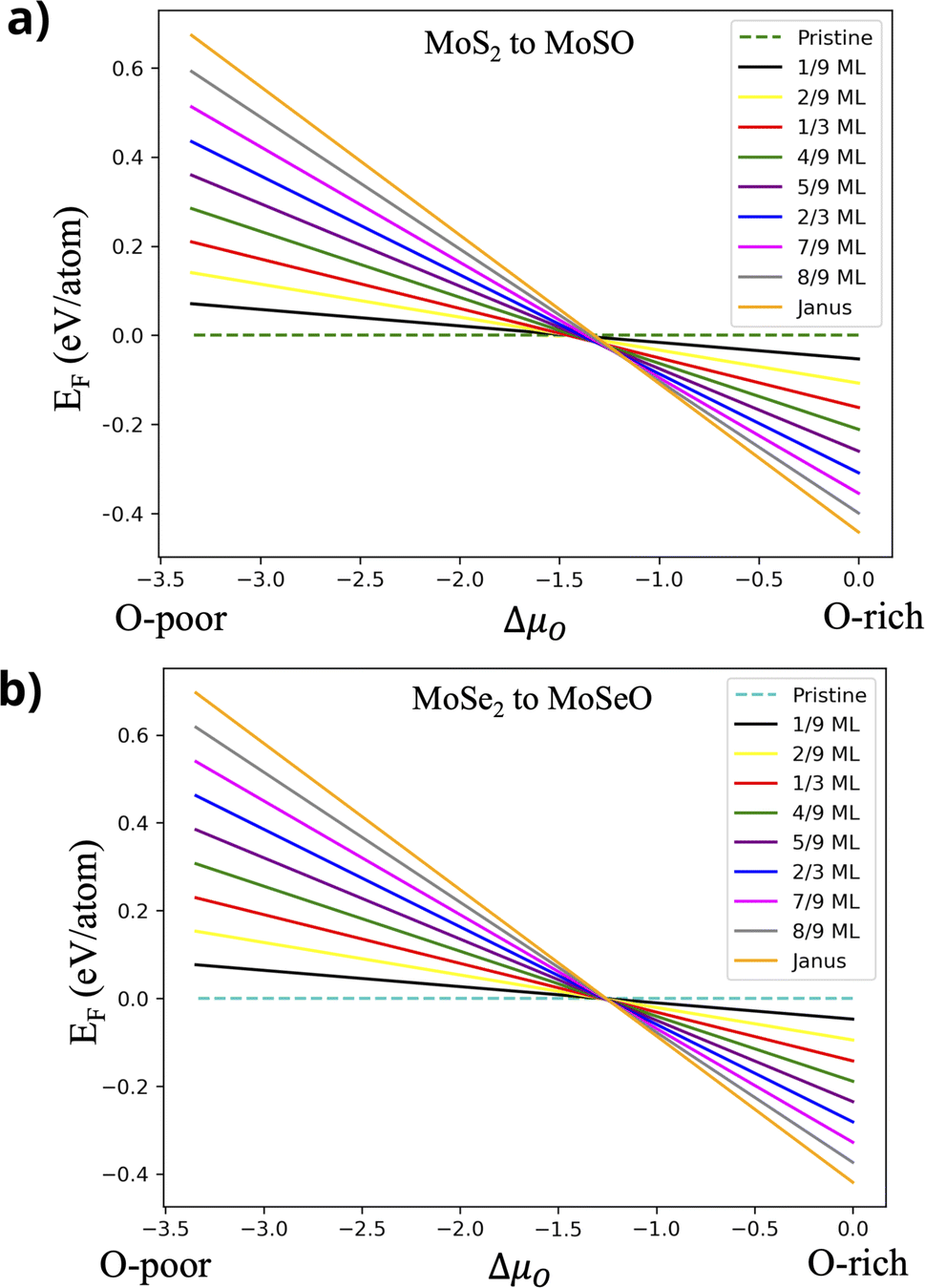 | ||
| Fig. 3 Formation energies vs. oxygen chemical potential, including all oxidation steps. (a) From MoS2 to MoSO and (b) from MoSe2 to MoSeO. | ||
A similar behavior is observed in the case of MoSe2−γOγ; see Fig. 3b. Under oxygen-rich conditions, the stability follows the same trend as in the MoS2 case, increasing systematically as oxygen content does. When reducing the μO chemical potential from −1.5 to −1.0 eV (intermediate growth conditions), the most stable coverage changes from MoSeO to an oxygen coverage of 8/9 ML, after that to 7/9 ML and 2/3 ML, and finally reaches 1/3 ML. Out of this range, for more O-poor conditions, the most stable structure is the pristine MoSe2. As in the MoS2 case, the best way to obtain the MoSeO monolayer is by inducing growth in the presence of O-rich conditions.
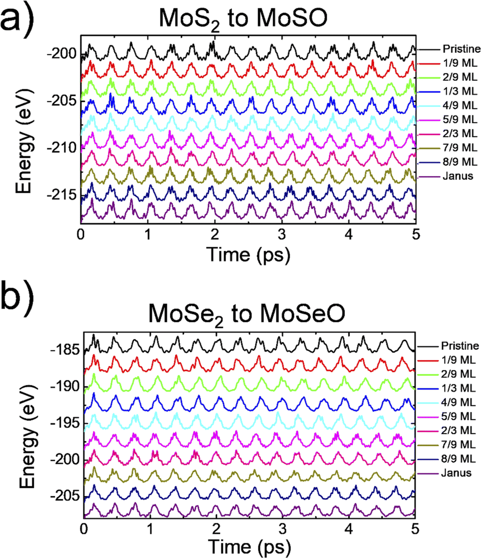 | ||
| Fig. 4 Ab initio molecular dynamics for the intermediate steps between pristine and Janus structures for (a) MoS2 and (b) MoSe2. | ||
3.4. Electronic properties
The semiconducting character of the monolayers has been extensively studied for their pristine phases (MoS2 and MoSe2), obtaining theoretical values for the direct band gap of 1.62 eV and 1.45 eV, respectively.32 Also, for the oxidized phases (MoSO and MoSeO), the oxidation of the monolayers has been shown to affect the electronic properties, specifically the band gap, resulting in values of 1.12 eV and 0.83 eV, respectively – going from direct to indirect character, in agreement with previous research (Table 2).10,26,32 We have undertaken the task of identifying the band-gap evolution at each stable oxidation step for both MoS2 and MoSe2. Fig. 5 shows coverage vs. gap energy for several stable oxidation steps. Notice that there is a clear trend, where the band gap gets reduced as oxygen coverage increases. Notice also that the difference between the band gaps in the pristine structures is 0.17 eV (MoS2 and MoSe2), which is reduced to 0.06 eV for 1/3 MLs, and then it increases to 0.22 eV for 2/3 MLs. This tendency is maintained until complete oxidation. It further increases as it tends to behave more Janus-like in the 7/9 MLs O, 8/9 MLs, and Janus monolayers. Finally, the gap difference between MoSO and MoSeO is 0.29 eV. The data presented in Fig. 5 evidences a clear band-gap engineering induced by oxidation. | ||
| Fig. 5 Variation of band-gap energy for each oxidation process step in both monolayers, from pristine to Janus phases. | ||
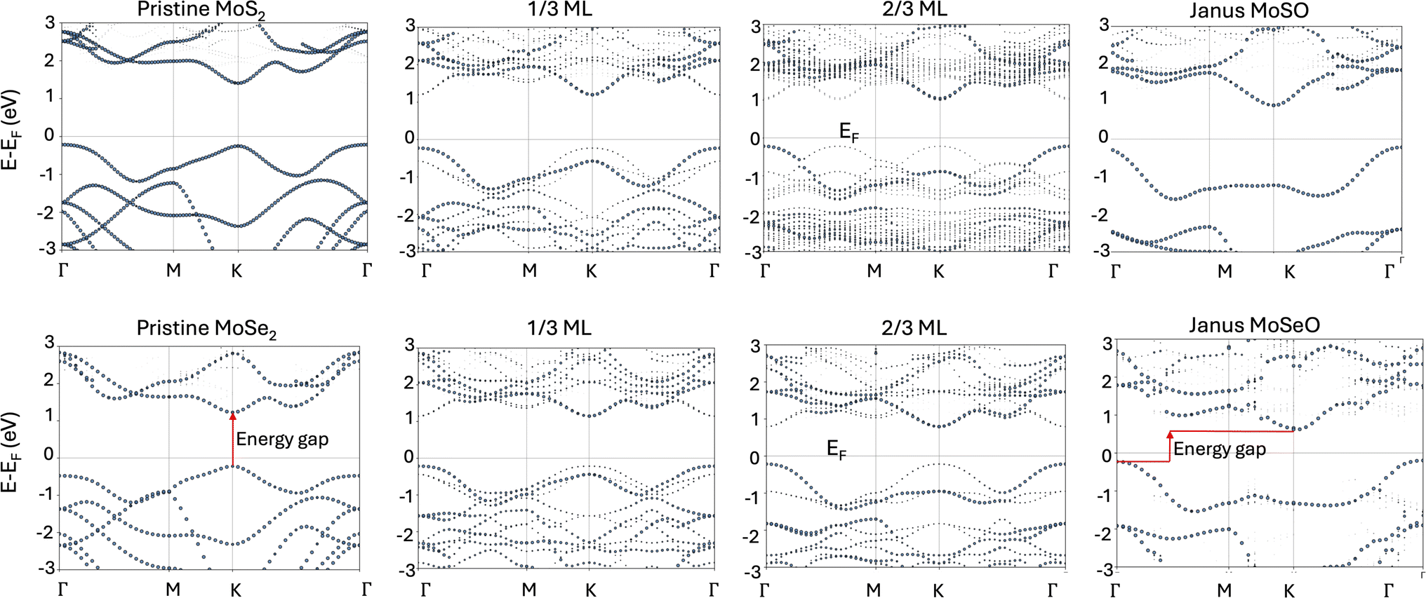 | ||
| Fig. 6 Effective band structures (unfolded bands) showing oxygen’s effect on the band gap at selected oxygen coverages. Zero energy defines the Fermi energy. | ||
We also calculated the projected density of states (PDOS), presented in the ESI† (Fig. S4 and S5), and the electrostatic potential isosurfaces (EPI), as shown in the next section.
Fig. 7a and e depict the EPI for the pristine MoS2 and MoSe2, respectively. In both cases, the Mo atoms show a green color, indicating that these atoms are neutral. Notice also that S zones (Fig. 7a) possess a larger charge accumulation than Se zones (Fig. 7e), an expected behavior since S is more electronegative than Se. Both top and down views of the monolayers are equivalent. Upon incorporating oxygen atoms in the S or Se sites, the system experiences a change in the EPI. In the top view of Fig. 7b and f, at 1/3 ML oxygen coverage, the diagonal turns completely red, meaning that a large charge accumulation is induced by the incorporated oxygen atoms; the remaining zones behave as described before. However, as the oxygen content increases to 7/9 ML (see top views of Fig. 7c and g), the charge accumulation zones increase, and the S or Se monolayer side (down views) is also affected due to the difference in electronegativity, turning more green reddish due to the charge density asymmetry induced by the oxygen atoms. Finally, when reaching the full oxygen coverage (1 ML), the charge density asymmetry is even larger, inducing a clear activity enhancement on the oxygen side, while the S (Fig. 7d) and Se (Fig. 7h) sides are more greenish.
 | ||
| Fig. 7 Electrostatic potential maps of pristine monolayers MoS2 and MoSe2 (a and e), partially oxidized phases (b, c, f and g), and Janus phases MoSO (d) and MoSeO (h) are presented. Red regions indicate a negative potential value, while blue regions indicate a positive potential value. | ||
The oxidation of the MoS2 and MoSe2 monolayers has led us to Janus phases of MoSO and MoSeO, which shows that the oxygen side is very reactive towards oppositely charged molecules (areas of positive electrostatic potential). Therefore, the oxidized Janus phase has potential applications in molecule traps or gas sensors.
4 Conclusions
In this study, we carried out a systematic analysis of the oxidation of transition metal dichalcogenide monolayers, namely MoS2 and MoSe2. We identified a pattern in the oxidation of the monolayers on a basal plane; after the incorporation of the first oxygen atom, subsequent oxygen atoms preferentially settled forming diagonal patterns before occupying the remaining positions. The formation energies demonstrated that several oxidized structures stabilize under different growth conditions, but the Janus monolayers (MoSO and MoSeO) are stable under oxygen-rich conditions. The systematic incorporation of oxygen affected the electronic properties, reducing the band gap as the oxygen content increased. The direct-to-indirect band-gap transition happens at the early stages of oxidation. Also, sites where oxygen atoms were incorporated accumulated an excess of negative charge. In contrast, the non-oxidized basal plane tended to have sites with a lower negative charge. The oxygen incorporation increased the reactivity on the O-side due to oxygen's large electronegativity with respect to the chalcogen S and Se atoms. The increase in reactivity induced by oxygen atoms may be used to trap molecules with positive polarities.Data availability
The data supporting this article is accessible through the corresponding author upon a reasonable request.Conflicts of interest
There are no conflicts to declare.Acknowledgements
We thank DGAPA-UNAM projects IG101124, IA100624, and IN101523 for their financial support. Calculations were performed in the DGCTIC-UNAM Supercomputing Center, project no. LANCAD-UNAM-DGTIC-150, LANCAD-UNAM-DGTIC-368 and LANCAD-UNAM-DGTIC-422. We thank Aldo Rodriguez-Guerrero for their technical support and useful discussions.References
- A. Geim and K. Novoselov, The rise of graphene, Nat. Mater., 2007, 6, 183–191, DOI:10.1038/nmat1849.
- A. Kokabi, M. Bahramy and S. Babaee Touski, Spin and electronic property prediction of IV–V binary monolayers using deep knowledge transfer method, J. Magn. Magn. Mater., 2024, 590, 171602, DOI:10.1016/j.jmmm.2023.171602.
- S. Manzeli, D. Ovchinnikov, D. Pasquier, V. Yazyev and K. Andras, 2D transition metal dichalcogenides, Nat. Rev. Mater., 2017, 2, 17033, DOI:10.1038/natrevmats.2017.33.
- S.E. Kadantsev and P. Hawrylak, Electronic structure of a single MoS2 monolayer, Solid State Commun., 2012, 152, 909–913, DOI:10.1016/j.ssc.2012.02.005.
- A. Nourbakhsh, A. Zubair, R. N. Sajjad, K. G. A. Tavakkoli, W. Chen, S. Fang, X. Ling, J. Kong, M. S. Dresselhaus, E. Kaxiras, K. K. Berggren, D. Antoniadis and T. Palacios, MoS2 Field-Effect Transistor with Sub-10 nm Channel Length, Nano Lett., 2016, 16, 7798–7806, DOI:10.1021/acs.nanolett.6b03999.
- A. K. Singh, P. Kumar, D. J. Late, A. Kumar, S. Patel and J. Singh, 2D layered transition metal dichalcogenides (MoS2): Synthesis, applications and theoretical aspects, Appl. Mater. Today, 2018, 13, 242–270, DOI:10.1016/j.apmt.2018.09.003.
- B. Radisavljevic, A. Radenovic, J. Brivio, V. Giacometti and A. Kis, Single-layer MoS2 transistors, Nat. Nanotechnol., 2011, 6, 147–150, DOI:10.1038/nnano.2010.279.
- L. Hongsheng, H. Nannan and Z. Jijun, Atomistic insight into the oxidation of monolayer transition metal dichalcogenides: from structures to electronic properties, RSC Adv., 2015, 5, 17572–17581, 10.1039/C4RA17320A.
- J. Paez, R. Ponce, H. Fernández, D. Hoat, E. Murillo, M. Moreno, D. Galván and J. Guerrero, The effect of shape and size in the stability of triangular Janus MoSSe quantum dots, Sci. Rep., 2021, 11, 21061, DOI:10.1038/s41598-021-00287-6.
- T. Wang, M. Su, H. Jin, J. Li, L. Wan and Y. Wei, Optical, Electronic, and Contact Properties of Janus-MoSO/MoS2 Heterojunction, J. Phys. Chem. C, 2020, 124, 15988–15994, DOI:10.1021/acs.jpcc.0c04042.
- A.-Y. Lu, H. Zhu, J. Xiao, C.-P. Chu, Y. Han, M.-G. Chiu, C.-C. Cheng, C.-W. Yang, K.-H. Wei, Y. Yang, Y. Wang, D. Sokaras, D. Nordlund, P. Yang, A.D. Muller, M.-Y. Chou, X. Zhang and L.-J. Li, Janus monolayers of transition metal dichalcogenides, Nat. Nanotechnol., 2017, 12, 744–749, DOI:10.1038/nnano.2017.100.
- M. Yagmurcukardes and F. M. Peeters, Stable single layer of Janus MoSO: Strong out-of-plane piezoelectricity, Phys. Rev. B, 2020, 101, 155205, DOI:10.1103/PhysRevB.101.155205.
- M. H. Rahman, E. H. Haque and S. Hong, High temperature oxidation of monolayer MoS2 and its effect on mechanical properties: A ReaxFF molecular dynamics study, Surf. Interfaces, 2021, 26, 101371, DOI:10.1016/j.surfin.2021.101371.
- H. S. Waheed, H. Ullah, M. W. Iqbal and Y. H. Shin, Optoelectronic and photocatalytic properties of Mo-based Janus monolayers for solar cell applications, Optik, 2022, 271, 170071, DOI:10.1016/j.ijleo.2022.170071.
- H. S. Waheed, M. Asghar, H. S. Ahmad, T. Abbas, H. Ullah, R. Ali, M. J. Iqbal Khan, M. W. Iqbal, Y.-H. Shin, M. Sheraz Khan and R. Neffatim, Janus MoSO and MoSSe Monolayers: A Promising Material for Solar Cells and Photocatalytic Applications, Phys. Status Solidi B, 2023, 260, 2200267, DOI:10.1002/pssb.202200267.
- P. Giannozzi, S. Baroni, N. Bonini, M. Calandra, R. Car, C. Cavazzoni, D. Ceresoli, G. L. Chiarotti, M. Cococcioni, I. Dabo, A. Dal Corso, S. de Gironcoli, S. Fabris, G. Fratesi, R. Gebauer, U. Gerstmann, C. Gougoussis, A. Kokalj, M. Lazzeri, L. Martin-Samos, N. Marzari, F. Mauri, R. Mazzarello, S. Paolini, A. Pasquarello, L. Paulatto, C. Sbraccia, S. Scandolo, G. Sclauzero, A.P. Seitsonen, A. Smogunov, P. Umari and R. M. Wentzcovitch, QUANTUM ESPRESSO: a modular and open-source software project for quantum simulations of materials, J. Phys.: Condens. Matter, 2009, 21, 395502, DOI:10.1088/0953-8984/21/39/395502.
- P. Giannozzi, O. Andreussi, T. Brumme, O. Bunau, M. Buongiorno, M. Calandra, R. Car, C. Cavazzoni, D. Ceresoli, M. Cococcioni, N. Colonna, I. Carnimeo, A. Dal Corso, S. Gironcoli, P. Delugas, J. DiStasio, A. Ferretti, A. Floris, G. Fratesi, G. Fugallo, R. Gebauer, U. Gerstmann, F. Giustino, T. Gorni, J. Jia, M. Kawamura, H. Y. Ko, A. Kokalj, E. Küçükbenli, M. Lazzeri, M. Marsili, N. Marzari, F. Mauri, N. Nguyen N, H. Nguyen, A. Otero-de-la-Roza, L. Paulatto, S. Poncé, D. Rocca, R. Sabatini, B. Santra, M. Schlipf, A. Seitsonen, A. Smogunov, I. Timrov, T. Thonhauser, P. Umari, N. Vast, X. Wu and S. Baroni, Advanced capabilities for materials modelling with Quantum ESPRESSO, J. Phys.: Condens.Matter, 2017, 29, 465901, DOI:10.1088/1361-648X/aa8f79.
- P. Giannozzi, O. Baseggio, P. Bonfà, D. Brunato, R. Car, I. Carnimeo, C. Cavazzoni, S. Gironcoli, P. Delugas, F. Ferrari Ruffino, A. Ferretti, N. Marzari, I. Timrov, A. Urru and S. Baroni, Quantum ESPRESSO toward the exascale, J. Chem. Phys., 2020, 152, 154105, DOI:10.1063/5.0005082.
- A. Dal Corso, Pseudopotentials periodic table: From H to Pu, Comput. Mater. Sci., 2014, 95, 337–350, DOI:10.1016/j.commatsci.2014.07.043.
- J. Perdew, K. Burke and M. Ernzerhof, Generalized Gradient Approximation Made Simple, Phys. Rev. Lett., 1996, 77, 3865–3868, DOI:10.1103/PhysRevLett.77.3865.
- G. Kresse and J. Hafner, Ab initiomolecular dynamics for liquid metals, Phys. Rev. B: Condens. Matter Mater. Phys., 1993, 47(1), 558–561, DOI:10.1103/physrevb.47.558.
- S. Grimme, J. Antony, S. Ehrlich and H. Krieg, A consistent and accurateab initioparametrization of density functional dispersion correction (DFT-D) for the 94 elements H-Pu, J. Chem. Phys., 2010, 132(15), 154104, DOI:10.1063/1.3382344.
- S. Nosé, A unified formulation of the constant temperature molecular dynamics methods, J. Chem. Phys., 1984, 81, 511–519, DOI:10.1063/1.447334.
- W. G. Hoover, Canonical dynamics: Equilibrium phase-space distributions, Phys. Rev. A, 1985, 31, 1695, DOI:10.1103/PhysRevA.31.1695.
- J. A. Wilson and A. D. Yoffe, The transition metal dichalcogenides discussion and interpretation of the observed optical, electrical and structural properties, Adv. Phys., 2006, 18, 193–335, DOI:10.1080/00018736900101307.
- V. Van On, D. Khanh Nguyen, J. Guerrero-Sanchez and D. M. Hoat, Exploring the electronic band gap of Janus MoSeO and WSeO monolayers and their heterostructures, New J. Chem., 2021, 45, 20776–20786, 10.1039/D1NJ04427C.
- H. Liu, N. Han and J. Zhao, Atomistic insight into the oxidation of monolayer transition metal dichalcogenides: from structures to electronic properties, RSC Adv., 2015, 5, 17572–17581, 10.1039/C4RA17320A.
- D. K. Nguyen, J. Guerrero-Sanchez, V. Van On, J. F. Rivas-Silva, R. Ponce-Pérez, G. H. Cocoletzi and D. M. Hoat, Tuning MoSO monolayer properties for optoelectronic and spintronic applications: effect of external strain, vacancies and doping, RSC Adv., 2021, 11(56), 35614–35623, 10.1039/D1RA05639E.
- V. Van On, D. K. Nguyen, J. Guerrero-Sanchez and D. M. Hoat, Exploring the electronic band gap of Janus MoSeO and WSeO monolayers and their heterostructures, New J. Chem., 2021, 45(44), 20776–20786, 10.1039/D1NJ04427C.
- M. Hillert, The compound energy formalism, J. Alloys Compd., 2001, 320, 161–176, DOI:10.1016/S0925-8388(00)01481-X.
- Q. Guo-Xin, M. Martin and D. Chadi, Phys. Rev. B: Condens. Matter Mater. Phys., 1988, 38, 7649, DOI:10.1103/PhysRevB.38.7649.
- A. Kumar and P.K. Ahluwalia, Electronic structure of transition metal dichalcogenides monolayers 1H-MX2 (M = Mo, W; X = S, Se, Te) from ab-initio theory: new direct band gap semiconductors, Eur. Phys. J. B, 2012, 85, 186, DOI:10.1140/epjb/e2012-30070-x.
- X. Wang, Y. Gong, G. Shi, W. Leong, K. Keyshar, G. Ye, R. Vajtai, J. Lou, Z. Liu, E. Ringe, B. Kang and M. Pulickel, Chemical Vapor Deposition Growth of Crystalline Monolayer MoSe2, ACS Nano, 2014, 8, 5125–5131, DOI:10.1021/nn501175k.
- A. Xie, H. Hao, C.-S. Liu, X. Zheng, L. Zhang and Z. Zeng, Giant tunnel electroresistance in two-dimensional ferroelectric tunnel junctions constructed with a Sc2CO2/In2Se3 van der Waals ferroelectric heterostructure, Phys. Rev. B, 2023, 107(11), 115427, DOI:10.1103/physrevb.107.115427.
- V. Popescu and A. Zunger, Effective Band Structure of Random Alloys, Phys. Rev. Lett., 2010, 104(23), 236403, DOI:10.1103/physrevlett.104.236403.
- J. You, Y.-S. Kim, K. C. Santosh and K. Cho, Monolayer MoS2 Bandgap Modulation by Dielectric Environments and Tunable Bandgap Transistors, Sci. Rep., 2016, 6, 29184, DOI:10.1038/srep29184.
- S. K. Pandey, R. Das and P. Mahadevan, Layer-Dependent Electronic Structure Changes in Transition Metal Dichalcogenides: The Microscopic Origin, ACS Omega, 2020, 5, 15169–15176, DOI:10.1021/acsomega.0c01138.
Footnote |
| † Electronic supplementary information (ESI) available. See DOI: https://doi.org/10.1039/d4ra02928c |
| This journal is © The Royal Society of Chemistry 2024 |