
 Open Access Article
 This Open Access Article is licensed under a Creative Commons Attribution-Non Commercial 3.0 Unported Licence
A critical mini-review on doping and heterojunction formation in ZnO-based catalysts
Buzuayehu Abebe
 *,
Neeraj K. Gupta
and
Dereje Tsegaye
*
*,
Neeraj K. Gupta
and
Dereje Tsegaye
*
Department of Applied Chemistry, School of Applied Natural Science, Adama Science and Technology University, P.O. Box 1888, Adama, Ethiopia. E-mail: buzea8@gmail.com; detsegaye@gmail.com
First published on 29th May 2024
Abstract
This mini-review on doping and heterojunctions for catalysis applications provides a comprehensive overview of key aspects. Doping, when carried out adequately with a uniform distribution, creates a new energy level that significantly enhances charge transfer and light absorption. This new level alters the material's morphology and enhances intrinsic defects. For instance, ZnO, despite its exceptional band edge concerning oxygen reduction and water oxidation redox potentials, faces the issue of electron–hole recombination. However, forming a heterojunction can effectively aid charge transfer and prolong electron–hole relaxation without recombination. This is where the role of doping and heterojunctions becomes crucial. Additionally, incorporating noble metals with S- and Z-scheme heterojunctions offers a promising mechanism for charge transfer and visible light harvesting, further amplifying the catalytic properties.
 Buzuayehu Abebe | Dr Buzuayehu Abebe is a prominent researcher specializing in nanomaterials for wastewater treatment and biomedical applications. His research contributes significantly to health and human welfare, reflecting a strong commitment to addressing critical societal challenges. With over forty (40) published research and review articles, Dr Abebe has established himself as a leading authority in his field. Additionally, he holds key editorial roles and serves as a reviewer for prestigious publishers such as the Royal Society of Chemistry (RSC), the American Chemical Society (ACS), Elsevier, and Springer. Dr Abebe's dedication to advancing scientific knowledge is exemplified by his extensive review work, which has encompassed over 200 manuscripts for various high-impact journals. |
 Neeraj K. Gupta | Neeraj Gupta has a master's degree in Polymer Science and Technology from Lancaster University, U.K., and a Ph.D. from Harcourt Butler Technological Institute and Shriram Institute for Industrial Research, Kanpur University. He has extensive global R&D experience in the industry and is currently a Professor of Polymer Science and Technology in the Applied Chemistry Department at ASTU, Ethiopia. His research interests include polymer processing, radiation processing, nanotechnology, and recycling. He has supervised eight master's and seven Ph.D. theses, has 71 research and conference papers, and holds five patents. |
 Dereje Tsegaye | Dr Dereje Tsegaye has served in industry, academics and research for more than three decades. He is currently working as Associate Professor, Department of Applied Chemistry, Adama Science and Technology University, Adama, Ethiopia, East Africa. Dr Dereje has published 15 research articles in national and international journals and presented some papers in national and international conferences. He has taught various chemistry courses to UG, PG, and PhD students in various Ethiopian universities and supervised more than 20 M.Sc. and 1 Ph.D. students. He is currently supervising 4 M.Sc. and 3 Ph.D. students. His research is mainly focused on the synthesis and application of environment friendly nanomaterials. |
Introduction
ZnO, among several semiconductor catalysts, stands out due to its unique properties. It has more positive potential than the redox potential of water and more negative potential than the redox potential of oxygen.1 Applying ZnO in a photocatalytic reaction can reduce oxygen and oxidize water molecules to generate an oxidizing agent. ZnO has high redox potential, better chemical and physical stability at high temperatures, good defect chemistry, and a considerable excitonic binding energy of 60 meV.2 Among the three crystal structures of ZnO, wurtzite is thermodynamically stable. Besides, ZnO is also the richest family of nano morphological structures, which is beneficial for diverse applications.3 However, electron–hole recombination and inadequate visible light absorption are the two main drawbacks of ZnO. This review focuses on ZnO as a host material.Doping and creating heterojunctions are commonly used to modify the properties of ZnO. These modifications include extending its ability to absorb visible light and reducing electron–hole recombination (EHR). The band gap of ZnO needs to be reduced to capture visible light, which constitutes about 40% of the solar spectrum. Doping introduces a mid-gap energy level within the valence band (VB) and conduction band (CB) of ZnO,4,5 facilitating electron–hole transfer between semiconductors to achieve stability or reduce their thermodynamic energies.6,7 Forming a heterojunction between semiconductors with different band gap values can enhance the charge transfer mechanism. Techniques such as XRD, PL, DRS-UV-vis, XPS, and STEM are commonly used to understand the effects of dopants, and Mott–Schottky analysis, DRS-UV-vis, XPS, and EPR are used to realize charge transfer mechanisms within heterojunction interfaces.8–10 Doped ZnO exhibits low and high-angle peak shifts compared to the host ZnO in XRD patterns. The low-angle shift is attributed to including larger ionic-radius dopants, while the shift towards a higher angle is due to including smaller ionic radii dopants.11,12 Doped ZnO shows reduced PL intensity compared to host ZnO, indicating diminished electron and hole recombination due to interactions between the host sp and dopant d states.13,14 The reduction in intensity of the DRS-UV-vis spectra for doped ZnO is linked to extended visible light absorption. XPS also reveals a lower binding energy shift for doped ZnO than the ZnO host. STEM, equipped with different detectors, can show the substitution and scattering of the dopant on the host surface.15
Many research publications have tried to understand the changes in properties that occur when dopants are added to the host matrix and when heterojunctions are formed. However, there is a need for better mutual understanding and agreement among these publications. This summary highlights the changes in properties due to doping and heterojunctions, drawing on the authors' extensive experience and a recently published literature survey. It starts by exploring the basics of heterojunctions and doping, followed by a detailed discussion and key concepts based on relevant articles. The focus is specifically on metal ion doping and metal or metal oxide heterojunctions for clarity and comprehension.
Fundamentals of doping and heterojunction
Photocatalysis is a surface reaction that occurs when light irradiates a surface, causing the separation of electrons and holes. Once the electrons absorb light, they excite to the first excitatory state within a few femtoseconds. The excited elections precede vibrational relaxation in picoseconds and then return to the ground state through fluorescence within nanoseconds. The resulting photon-induced electron and hole pairs should have significant reduction and oxidation potentials and be trapped in metastable states. For an efficient photocatalysis reaction, the photon-induced electron–hole recombination should decrease, and the pairs should migrate to the surface and react with surface-sorbed pollutant molecules.16 Additionally, for these surface reactions, the band edge position of the catalyst relative to the oxidation and reduction redox potential is a critical consideration. The catalyst valence band (VB) and conduction band (CB) edges should have more positive and negative potential than the redox potential of water and oxygen, respectively. Wurtzite ZnO, with a wide band gap of 3.23 eV, possesses excellent optoelectronic and piezoelectric properties. Its hexagonal crystal structure has lattice parameters of a = 0.3296 nm and c = 0.520 nm, and it belongs to the P63mc (Hermann–Mauguin) or C46v (Schoenflies notation) space group.17 ZnO has a CB potential of −0.5 V and a VB potential of +2.7 V versus a standard hydrogen electrode (NHE). The CB potential is more negative than the reduction redox potential of O2/˙O2− (−0.33 V), while the VB potential is more positive than the oxidation redox potential of ˙OH/H2O (Fig. 1).18 Therefore, O2 and H2O can be easily reduced and oxidized in the presence of electrons and holes.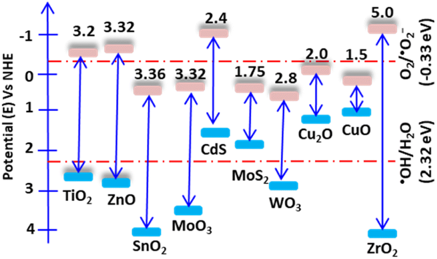 | ||
| Fig. 1 Band edge potentials and band gap of some selected semiconductors. The band edge potentials are shown relative to water and oxygen's oxidation and reduction potentials, respectively. | ||
However, applying single ZnO as a photocatalyst has several drawbacks, such as photon-generated electron–hole recombination (EHR) and inadequate solar energy absorption. Pure ZnO has some drawbacks when used as a photocatalyst, such as electron–hole recombination (EHR) and insufficient solar energy absorption. High electron density differences between the VB and CB cause the semiconductor's EHR.19 Depending on various conditions, recombination can occur internally or on the catalyst's surface.
Forming a heterojunction can reduce external EHR, while impurity doping can reduce internal recombination by creating new energy levels within the host energy gap. Besides, the EHR also produces heat in the surrounding medium, which diminishes the sorption of pollutant molecules on the catalyst surface. In the case of solar energy absorption, wide-bandgap materials such as ZnO are activated only by UV light (about 4% of the total solar spectra).20 As a result, ZnO photocatalytic performance under visible solar light irradiation is poor. These single semiconductor material drawbacks can be improved by dopant inclusion in the host lattice and forming a heterojunction.
Doping is a process of VB elevation, CB lowering, or creating localized energy levels with the host band gap. Depending on the dopant and host work functions, dopants can be acceptors or donors. The dopant, which has a lower work function than the host, acts as a donor type and donates electrons to the host CB. The dopant, which has a greater work function than the host, acts as an acceptor type and accepts electrons from the host CB.21 Defects created very near the VB and CB are shallow acceptor and shallow donor levels. While defects created by the VB and CB are deep holes and deep electron traps22 (Fig. 2). The major dopant inclusion positions in the host matrix are interstitial, substitution, and segregation.
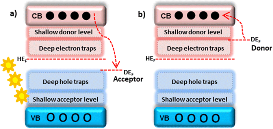 | ||
| Fig. 2 (a) Acceptor; (b) donor-type defects. The shallow donor and acceptor cavities are located near the CB and VB, respectively. The deep electron and deep hole trap defects were created next to the shallow-level defects of CB and VB, respectively. | ||
These positions depend on factors such as dopant amount, electronegativity, and ionic radii.23 Morphology changes, defects, and deformations also form during doping, essential for different applications.
Forming a heterojunction involves aligning the bands of semiconductors with different band structures, and it is one of the most effective ways to separate photon-induced electron–hole pairs.24 Various heterojunction mechanisms, such as the Z-scheme, M-scheme, S-scheme, and staggered type, have been proposed to prolong the lifetime of electrons and holes. When two semiconductors form a heterojunction, three main cases typically occur. First, electronic densities and Fermi levels are redistributed until an equilibrium state is reached, followed by the development of an internal electric field, or accumulated layer, between the two semiconductor interfaces. Finally, band edge bending occurs, which can create allowed and forbidden charge transfer pathways within the semiconductor interfaces.
The separation of electron–hole pairs, the surrounding charge density, and the charge transfer process impact a material's local chemical properties and flat band potentials from the standard position.25 Therefore, it is essential to study the electronic structure and type of semiconductor to assess the heterojunction properties of a material. The Mott–Schottky plot analysis provides information on whether the material is n-type or p-type and on the material's band edges. The n-type and p-type characteristics can be easily determined from the positive and negative slopes of the Mott–Schottky plot, respectively. The CB of materials can be determined from the flat band potentials (vs. NHE) by extrapolating the Mott–Schottky plot towards the x-axis. With the CB from the Mott–Schottky plot and the bandgap from the DRS-UV-vis analysis, the valence band (VB) can be calculated using the formula VB = Eg + CB, where VB, CB, and Eg represent the valence band, conduction band, and energy gap (bandgap) of the material.26 Additionally, it is possible to use a combination of Mott–Schottky and ultraviolet photoelectron spectroscopy to determine the flat band potentials. The relative intensity vs. binding energy ultraviolet photoelectron spectroscopy (UPS) plot can provide the VB potential of the material directly. Then, the CB can be easily determined from the DRS-UV-vis bandgap and VB values.27 XPS analysis can determine the direction of charge transfer by observing the shift in binding energy associated with a change in the charge density over the target element. A lower binding energy shift indicates an increase in charge density, while a higher binding energy shift indicates a decrease in charge density over the specific element. Therefore, a lower shift indicates charge transfer towards that particular element, and a higher shift indicates charge transfer from the target element to the other attached semiconductor.28
Doping
Extrinsically and intrinsically, defects in the host lattice create a material with different optoelectronic and magnetic properties. Materials with a high dopant concentration in the host matrix generate magneto–optoelectronic and optoelectronic properties. Thus, the materials have electron spin and electron charge properties. These electron spin and electron charge properties are advantageous in various fields, such as information recording and solar cells. The optical properties change due to the sp–d host–dopant exchange interaction and magnetic properties due to free electrons in the dopant 3d state, which results in band gap deformation.29 Doping transition metals (which have unfilled d or f orbitals) creates mid-gap energy levels without changing the band gap of the host.4,5 The created mid-gap benefits the electronic transition and relaxation of holes and electrons without recombination. The holes and electrons react with water and oxygen to generate reactive oxygen species, which are beneficial in numerous fields. The expected common transitions within doped material include the VB–CB host transition, the d–d dopant transition, the host CB–dopant d transition, and the host VB–dopant d transition.30 However, there is a solubility problem, especially with metal ions (p-type) in the host semiconductors. For example, rare earth metals have a greater ionic size than Zn, which makes their solubility in the ZnO lattice more difficult. Transition metals (TMs) have comparable ionic sizes and good solubility.31 Because of perfect incorporation, the hexagonal crystal structure of ZnO cannot be altered by doping with TMs. Instead, doping affects the unit cell volume and lattice parameters due to the stress created within the crystal structure.32 Doping metal ions also leads to changing the morphology, creating different defects, and increasing the surface area of the materials.33 However, the formation of over-aggregation and the development of grain boundaries at high concentrations may lead to increasing particle and grain sizes.Optical properties
The improvement in the optical properties of ZnO based on the doping of TM elements results from the interaction between doped 3d electrons with the s or p host electrons (s–d or p–d).29 Photoluminescence (PL) and DRS-UV-vis are the most common techniques used to understand the optical properties of doped materials. Near-band edge emission (NBE) commonly occurs in the PL spectra at about 380 nm. This NBE emission is a characteristic property of ZnO and occurs due to direct EHR. Besides, the typical broad peak of ZnO PL spectra in the visible region is due to intrinsic defects created during synthesis.34 The decrease in intensity and wavelength shift are the two leading indicators of doping in PL spectra. The decline in emission intensity indicates a reduction in EHR due to the formation of defects within the band gap of the host. Defect peaks may increase during dopant inclusion, which supports the formation of more defects.35 At the same time, the shift towards a longer wavelength is also due to the sp–d exchange interaction, which results in a band gap change.36 The defects may be intrinsic (without other impurities) or extrinsic due to the inclusion of impurities. They can act as an electron trapper in the CB after excitation and in the VB during excitation. Intrinsic defects include zinc vacancy (VZn, emitting violet light at 410–420 nm, with energy of 3.02 eV),37 zinc interstitial (Zni, emitting UV light at 380–400 nm, with energy of 3.30–3.34 eV), zinc antisite (OZn, emitting light at 520 nm, with energy of 2.38 eV), and oxygen interstitial (Oi, emitting light at 540 nm, with energy of 2.23 eV).38 Other intrinsic defects are oxygen vacancy (VO, emitting light at 500–520 nm, with an energy of 2.43 eV),39 and oxygen antisite (ZnO). The intrinsic ZnO defect peaks are related to the electron donor (VO and Zni) and acceptor (VZn and Oi) levels. These donor and acceptor levels occur below the CB and above the VB of the host energy gap, respectively. Luminescence emission bands such as violet-blue emission related to electron transition between Zni and host VB, blue between VZn and host CB, green between VO and VZn, and yellow associated with recombination of holes trapped in Oi and electrons in the CB were observed. The extrinsic defects occur as a result of TM impurities doping.Magnetic properties
The magnetic properties of semiconductors are of interest to electronic devices today. ZnO has fully filled Zn d-orbitals, which are diamagnetic by nature. The magnetic properties of ZnO are due to defects created during synthesis, which arise from local spin exchange through the vacancies.40 Of course, the magnetic properties of ZnO depend on the synthesis method41 and calcination temperature. Different models have explained the reasons for enhancements in the magnetic behavior of doped materials.According to the Ruderman–Kittel–Kasuya–Yosida (RKKY) model, it results from the host-mediated, well-aligned coupling of spin-polarized magnetic electrons within dopant elements. The second is the bound magnetic polarons (BMP) model, which explains the magnetic properties of doped materials based on the parallel alignment of localized spins and carriers of dopants due to exchange interactions. The third spin-split impurity band model explains the magnetic properties based on the splitting of the dopant band and then its interaction with the 3-d state.42 Of course, doped materials' magnetic properties depend on several factors, such as dopant amount, temperature, and dopant type. In general, for ferromagnetism properties, the following three requirements are needed: (i) the net electron spin in the incomplete d shell of an atom; (ii) the interaction of this d shell electron spin of the host atom with adjacent d shells of dopant, which leads to antiferromagnetic properties; and (iii) spin coupling between incomplete d shells with conduction band electrons in the form of ferromagnetism.43
The change in magnetic properties can be understood using different analytical techniques. The EPR technique is one of the sensitive techniques used to detect the intrinsic and extrinsic defects created. For example, the electron paramagnetic resonance (EPR) spectra for the ZnO signal at g = 1.960 are due to the oxygen interstitial, and the oxygen and Zn vacancy signal at g = 2.006 is due to the surface defects.44 The technique can show other signals for extrinsic doping both in the core and surface regions. This signal depends on the material characteristics, the hyperfine coupling of spin, and the size of the particles. Of course, the signal intensity varies with the dopant amount and decreases as the amount increases due to increased doped ion interaction. The spin-trapping EPR analysis is also essential to understand the creation of ˙O2− and ˙OH species in the presence of 5-dimethyl-1-pyrrolidine N-oxide (DMPO) based on the DMPO–˙O2− and DMPO–˙OH signals that are detected in the EPR spectra.
Transition metal doping
Alsmadi et al.13 conducted detailed XPS and PL analyses to confirm the inclusion of Mn in the ZnO lattice without affecting the würtzite structure of the host ZnO. XPS analysis showed that the oxygen vacancy concentration could be controlled by calcinating the materials in vacuum and air. When the sample was calcinated under vacuum, the oxygen vacancy peak increased, and in air, it decreased. The increase in vacuum confirmed the creation of defects, and the decrease in air showed the filling of oxygen defects by oxygen from the air. PL analysis showed a deep-level emissions peak in the visible region. The intensity increase for the green band with the dopant amount indicated an increase in oxygen vacancy concentration. In the same analysis, intense near-band-edge (NBE) shifted towards a longer wavelength (red shift), signifying the incorporation of Mn in the ZnO host lattice. Besides, all doped materials with different Mn dopant concentrations showed ferromagnetic ordering properties. The ferromagnetic property was mainly due to the oxygen vacancies created during doping, which increased as the doping concentration increased. A slight low-angle XRD pattern shift was also confirmed for Mn-doped ZnO compared to ZnO. This shift resulted from slight unit cell expansion due to the greater ionic radii of Mn.
Ali et al.48 also conducted a detailed theoretical and experimental study on Mn-doped ZnO. The study confirmed the ferromagnetism properties of Mn–ZnO material to be due to zinc vacancy (VZn). The presence of defects in the doped material was analyzed using XPS. The analysis used different concentrations of argon and oxygen atmospheres (20 Ar/80 O2 and 80 Ar/20 O2 atmospheres). The shifting of Zn 2p3/2 and Zn 2p1/2 peaks towards higher binding energy for doped materials in the presence of a lower argon atmosphere confirmed the domination of VZn. In addition, the PL analysis showed a peak at 410 nm, mainly due to the electron transition from VZn levels to the ZnO host CB. Another peak at 570 nm was associated with the VO defect.
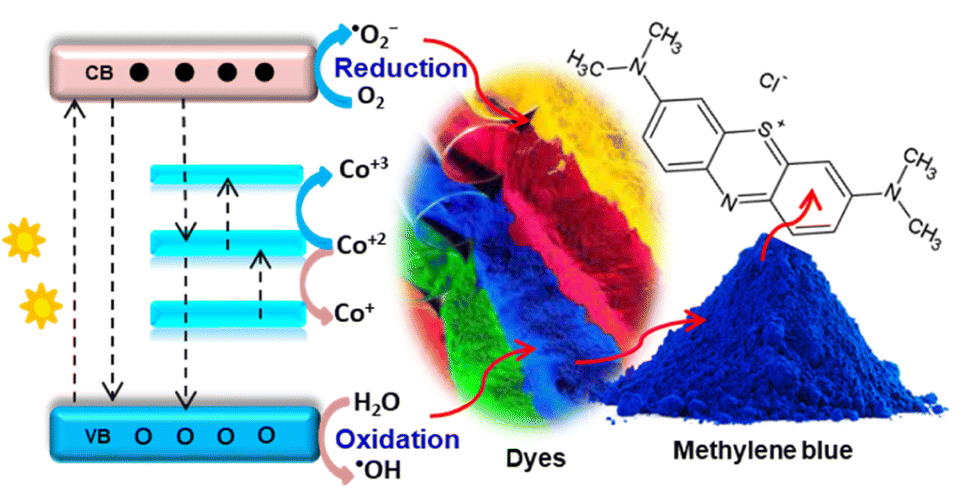 | ||
| Fig. 3 Scheme showing probable charge transfer within cobalt-doped ZnO: valence to conduction band, cobalt(III) level to host conduction band, cobalt(III) to host valence band, and dopant d–d transition. The charge transfer enhances the electron–hole relaxation time and degrades dye pollutants such as methylene blue by oxidising agents. | ||
This extrinsic inclusion of Co2+ ions in the ZnO lattice is due to the s–d or p–d exchange interaction between the host band electron and 3d localized dopant electrons, creating a new energy level. The study also reported that a host lattice strain was created with an increased Co amount, resulting in cluster formation, morphological change, and enhanced defect density. Chen et al.51 also obtained three absorption bands in the visible region attributed to Co2+ d–d electronic transitions, indicating the proper substitution of Zn by Co2+ ions without affecting the host ZnO structure. The band gap analysis using the Kubelka–Munk function confirmed the presence of two regions for UV and visible light absorption.
The VB maxima, CB minima, Fermi tail, Fermi level, cut-off tail, and band gap were determined by ultraviolet photoelectron spectroscopy. This confirmed the dominance of VB maxima by the O-2p orbital and the increase of CB minima by Co atoms. The study also confirmed the formation of a mid-state band gap to enhance visible light absorption.
Chehhat et al.52 used the sol–gel method to synthesize Co–ZnO with a porous structure. The PL analysis showed a band edge shift towards a higher wavelength than single ZnO. This shift indicated the presence of s–d and p–d exchange interactions due to the Co interchange by Zn. The PL analysis by Kaphle et al.53 showed an intensity reduction with increased Co concentration. This intensity reduction indicated a reduction in electron–hole recombination due to the dopant acting as an electron sink. The PL spectra of ZnO showed a broad, small peak in the visible region due to intrinsic defect-related green emission. The intensity of the broad emission peak increased with Co concentration, indicating the formation of more defects. Chanda et al.54 also reported an increase in defect-related emission peak intensity with an increase in Co amount, indicating an increase in defects. The PL analysis by Kaphle et al.53 also showed an increase in NBE emissions and a decrease in visible emissions. Besides, the calcination temperature affects both the formation of defects and crystallinity. An increase in temperature leads to an increase in EHR and crystallinity and a decrease in defect formation. However, high-temperature calcination in an oxygen-rich environment results in an oxidation process that increases oxygen content.
Doping with Co also tunes ZnO's magnetic properties due to cobalt's highest magnetic moments and positive magnetic exchange coupling constant. Kazmi et al.55 confirmed the ferromagnetic properties of Co–ZnO 1D nanowires. The ferromagnetic properties were confirmed based on the density functional theory analysis. The Co 3d spin-polarised electrons and host O-2p electron exchange integration caused the magnetic property. The intrinsic defects and substitution occurred without secondary Co-metal or Co3O4 phase formation. Salameh et al.56 confirmed the formation of defects (oxygen vacancies) by XPS. The analysis showed a unique peak at 531.0 eV, indicating the presence of electrons in the oxygen vacancies. The intensity of this peak increased as the Co concentration increased.
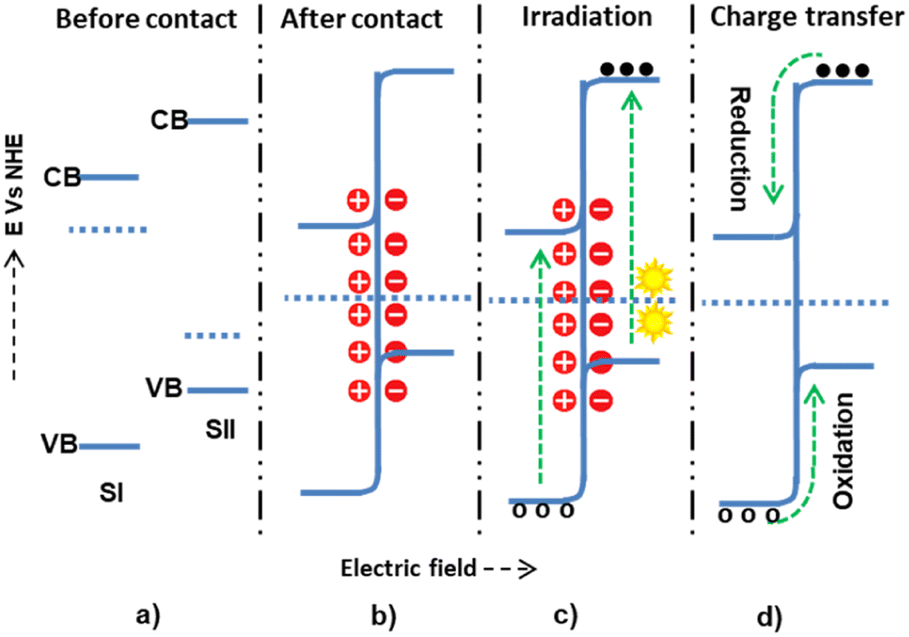
Heterojunction
The three conventional heterojunction photocatalysts are the straddling, staggered, and broken gaps. In the straddling gap heterojunction, the VB and CB of semiconductor I (SI) are higher than those of semiconductor II (SII). Thus, the electrons and holes collected at a lower redox potential have a greater chance of recombination. However, in the type II heterojunction, the CB and VB potentials of SI are higher than those of SII; this causes electrons to diffuse from SI to SII and holes from SII to SI, preventing the recombination process. In the type III heterojunction, the bandgaps of SI and SII do not overlap, making them unsuitable for charge separation. Therefore, the type II heterojunction is the most effective for photon-induced electron–hole pair separation and enhancing the photocatalysis application efficiency.In a staggered-type binary heterojunction, when solar light irradiates the semiconductors, electrons and holes are created in the CB and VB of the materials due to the matching band potential. The electrons and holes then move from the semiconductor with higher potential energy to the one with lower potential energy (Fig. 4).67 The work function of SII is higher (lower Fermi level) than that of SI. In this process, valence electrons are transferred from the semiconductor with higher potential energy to the one with lower potential energy, resulting in a built-in electric field at the interface. This electric field inhibits further electron transfer, facilitating electron and hole movement and inhibiting recombination. The internally built electric field is directed from SI to SII. Thus, electrons are transferred from SII's more negative potential to SI's less negative potential, and holes move from SI to SII. However, this junction type leads the electrons and holes to exist in positions of low reducing and oxidizing redox energy. This low redox energy is the main drawback of the type II mechanism.
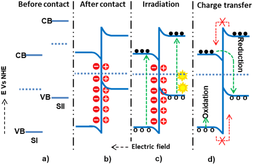 | ||
| Fig. 4 The possible type II (staggered type) charge transfer mechanism within semiconductor I and semiconductor II: (a and b) before and after contact, respectively; (c) during light irradiation and electron–hole generation; and (d) electron–hole migration. | ||
The type-II heterojunction (n–n heterojunction) has a slower electron–hole separation due to ultrafast electron–hole recombination behavior and reduction and oxidation reactions with lower potential and electrostatic repulsion. The properties of the heterojunction and the photocatalysis mechanism depend on the p-type and n-type characteristics and the semiconductors' CB and VB potentials.
Besides, there is also an electrostatic repulsion between the host and guest electrons and holes during transfer, which makes the transfer process more difficult.68
The p–n or n–p heterojunction was developed to address the n–n heterojunction problem by creating an additional electric field.69 In the n-type (SI) and p-type (SII) heterojunctions, the Fermi level of the p-type semiconductor is near the VB. As a result, electrons can move from the n-type semiconductor to the p-type semiconductor and holes from the p-type semiconductor to the n-type semiconductor until an equilibrium is reached. This movement of electrons and holes creates an internal electric field (space-charge region) before light irradiation, and the electric field potential at the interface allows electrons and holes to move in the opposite direction. The developed electric field facilitates a faster electron–hole charge transfer during light irradiation. Additionally, reduction and oxidation reactions occur at higher potentials than in the type II (n–n) heterojunction. The n–p heterojunction demonstrates effective charge separation, rapid transfer, and more electron–hole relaxation time. Electrons diffuse from SII to SI till the equilibration state in the p-type (SI) and n-type (SII) heterojunction. The built-in electric field changes direction from SII to SI and assists the electron–hole transfer process, similar to the n–p heterojunction. In the p-type (SI) and p-type (SII) heterojunction, the SII has a higher Fermi level than the SI. Thus, electrons diffuse from SII to SI up to the equilibration state. However, the movement of electrons from SII to SI is suppressed during light irradiation due to the development of a negative charge at the interface edge of SI and forbidden electron movement due to band bending. As a result, the CB electrons of SII and the VB holes of SI undergo a reduction and oxidation process, respectively.70
Zhang et al.71 proposed the staggered-type heterojunction between fluorinated TiO2 (F-TiO2) and ZnO. The CB of ZnO has a greater negative potential than F-TiO2, while the VB of ZnO has a greater positive potential than F-TiO2. Under light irradiation, the electron migrates from the CB of ZnO to the F-TiO2 CB and the hole from the F-TiO2 VB to the ZnO VB. Thus, recombination is inhibited, and the electron reacts with oxygen (reduction), and the hole reacts with water (oxidation). This electron–hole reaction then generates ˙O2− and ˙OH for the degradation of methyl orange dye better than single TiO2. The extended electron–hole relaxation time was analyzed using PL. The PL intensity peak for the composite was much lower than that of single F-TiO2, indicating the EHR hindrance.
Das et al.8 proposed the type II (staggered) mechanism within the ZnO–In2O3 interface for efficient charge transfer and photocatalytic degradation of methylene blue dye. In2O3 (2.8 eV) and ZnO are n-type semiconductors with 4.28 and 5.2 eV work function values, respectively. The obtained CB and VB values for ZnO were −0.29 eV and 2.87 eV, respectively. For In2O3, the obtained CB and VB were −0.63 eV and 2.19 eV, respectively. This band edge potential showed electron migration from the more negative potential CB of In2O3 to the less negative CB potential of ZnO. The hole migrated from ZnO's more positive VB potential to the less positive VB potential of In2O3. This mechanism diminished the EHR and led to oxygen reduction and water oxidation by electrons and holes.
The Z-scheme mechanism is the second, recently proposed, and somewhat better heterojunction between two or more semiconductors. SI has a higher work function (lower Fermi level) in this mechanism than SII, causing electrons to transfer from SII to SI until an equilibrium state arises. The internally built electric field is directed from SI to SII. The developed electric field also electrostatically attracts and recombines electrons from SI to SII. However, the band edge bending develops a forbidden electron transfer from SII to SI and a forbidden hole transfer from SII to SI.72 The electrons are transferred from the CB of SI and recombined with the holes of SII. However, the electrons and holes, which have high thermodynamic energies on the CB of SII and VB of SI, are left without transfer to accelerate the high reduction and oxidation processes, respectively73,74 (Fig. 5).
 | ||
| Fig. 5 The possible Z-scheme charge transfer mechanisms within semiconductor I and semiconductor II: (a and b) before-and-after contact; (c) during light irradiation and electron–hole generation; and (d) allowed and forbidden electron–hole migrations. | ||
Zhou et al.75 synthesized nest- and core-shell-structured ZnO/TiO2 with Z-scheme heterojunction. Using the XPS technique, the band edge positions were accurately determined. The study proposed that the CB potential of ZnO was more negative than that of TiO2, while the VB potential of TiO2 was more positive than the VB of ZnO. This heterojunction led to recombining the CB electrons from ZnO with the VB electrons of TiO2. Thus, the CB electrons of TiO2 and the VB holes of ZnO survived with high thermodynamic energy. The holes and electrons could react with water and oxygen and generate an oxidizing agent.
Song et al.9 also proposed the Z-scheme mechanism within the Ag2O/ZnO heterojunction. The band energies of ZnO and Ag2O were determined from Mott–Schottky analysis.
The VB of Ag2O and ZnO were obtained to be 2.14 and 1.91 eV, and their conduction bands were 0.94 and −1.79 eV (vs. NHE), respectively. Thus, based on this heterojunction, the staggered type and Z-schemes were proposed as possible mechanisms. From the EPR analysis, ˙O2− was understood to be the main oxidizing agent. However, in the case of the staggered type, the electrons accumulated on the CB of Ag2O could not reduce oxygen to ˙O2−. This was because its CB potential was more positive than the redox potential of oxygen to ˙O2−, which contradicting the EPR analysis. Thus, the study suggested the Z-scheme mechanism as the most probable mechanism. This meant that the CB Ag2O electron recombined with VB holes of ZnO, while ZnO CB electrons reduced oxygen, and the VB Ag2O hole oxidized water to produce oxidizing agent species.
Ruan et al.76 proposed the Z-scheme charge transfer mechanism within the CuO/ZnO heterojunction. The band-edge potentials of CuO and ZnO were determined using the Mott–Schottky plot. The CB positions for ZnO and CuO obtained were −0.27 and −0.92 eV, respectively, and the VB potential obtained was 3.01 and −0.49 eV vs. NHE. The work also proposed a possible type II (staggered type) charge transfer mechanism with this band edge potential. This meant that electrons could migrate from the CB of CuO to the CB of ZnO, while holes could migrate from the VB of ZnO to the VB of CuO. However, the CB potential of ZnO (−0.27) was more positive than the redox potential of O2/˙O2− (−0.33 eV), indicating that ZnO CB electrons could not reduce O2. In addition, the VB potential of CuO (−0.49 eV) was more negative than the standard redox potential of ˙O/H2O (−2.38 eV), indicating that CuO VB electrons could not oxidize H2O. Hence, the type II mechanism contradicted the composite's efficient photocatalytic acid orange 7 dye degradation ability. Consequently, the work chose the Z-scheme mechanism as a charge transfer mechanism. In this Z-scheme mechanism, the electrons from the CB of ZnO migrated and recombined with the hole on the VB of CuO. While the CuO CB electron and ZnO VB electrons are present with high thermodynamic energy to react with oxygen and water, respectively, and produce the pollutant-reducing agent species (˙O2− and ˙OH).
Fu et al.6 proposed the Z-scheme mechanism for ZnO/MoS2 heterojunction. In the composite of ZnO (3.37 eV), a wide band gap material, and MoS2 (1.8 eV), a narrow band gap material, the work function of ZnO (5.2 eV) was greater than that of MoS2. Electrons migrated from the CB of MoS2 to the ZnO CB, and the Fermi-level equilibrium stage was achieved. It was shown that the CB of MoS2 had more negative potential than the ZnO CB, and after irradiation, electrons migrated from the ZnO CB to the VB of MoS2 and recombined through the Z-scheme mechanism. Moreover, the available electrons and holes with high thermodynamic energy produced species such as ˙O2− and ˙OH by reacting with oxygen and water, respectively.
The main drawback of the Z-scheme mechanism is the loss of electrons and holes with low thermodynamic reduction and oxidation energy due to recombination.77 This drawback can be diminished using a proper charge mediator between the two semiconductors, including noble metals such as gold and silver, as illustrated in Fig. 6. The electrons and holes present at low thermodynamic energies can then be transferred to the noble metals, preventing recombination. The inclusion of noble metals has also been shown to show surface plasmon resonance (SPR) characteristics. This SPR property, which means the oscillation of electrons with the electric field, assists materials in extending visible light absorption (40% of the total solar spectrum). Besides, SPR also extends the life of separated excitons, which is beneficial for catalysis applications.78 However, in the presence of the noble metals between the semiconductors, the Fermi level of the three components is rearranged depending on the work function values and becomes complex.
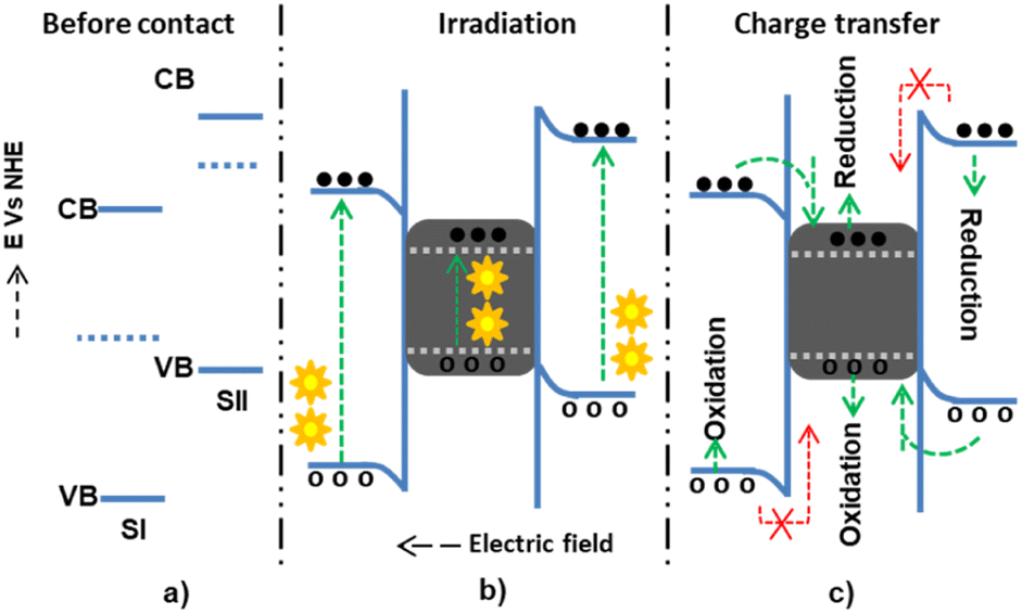 | ||
| Fig. 6 The possible Z-scheme charge transfer mechanism in the presence of noble metals within semiconductors I and II: (a) before contact; (b) during light irradiation and electron–hole generation in the existence of noble metal as an electron sink; and (c) allowed and forbidden electron–hole migration. | ||
Mahyoub et al.10 confirmed charge transfer within Ag–CeO2–ZnO composites based on photocurrent, PL, and electrochemical impedance spectroscopy (EIS) analysis. The XPS analysis showed shifts of the CeO2 and ZnO peaks in the composites compared to those of single ZnO and CeO2. The peak shifts indicated electron transfer from ZnO to CeO2. The reduction in PL spectra intensity for the composites compared to neat CeO2 and ZnO confirmed EHR hindrance, further verified by the highest photocurrent strength of the composites compared to single ZnO and CeO2. EPR analysis of the composites in the presence of DMPO as a radical trapping agent showed stronger EPR signals for both DMPO–˙O2− and DMPO–˙OH, indicating that they produced greater ˙O2− and ˙OH species than single ZnO and CeO2. The band edge positions of ZnO and CeO2 were determined, and the charge transfer mechanism was proposed. Ag metal in between acted as an electron conduction/transfer bridge to transfer electrons (through the Schottky barrier) from the ZnO CB to the CeO2 VB.
Additionally, silver Ag acts as a visible light absorber through the SPR effect, separating electron–hole pairs from ZnO and CeO2. Consequently, reduction occurs in the CB electrons of CeO2, while oxidation is observed in the VB holes of ZnO. Generally, semiconductor–metal heterojunction, or Schottky contact, is an effective method for improving charge separation. In this type of junction, the metal has a higher work function than the semiconductor, causing electrons to move from the semiconductor to the metal until reaching an equilibrium state upon contact. The metal is an electron sink during light irradiation, preventing recombination.79
Xu et al.80 proposed a mechanism somewhat different from the Z- and S-schemes and staggered-type heterojunction mechanisms for TiO2/ZnO/Ag heterojunction based on the work function. It was proposed that since the CB of ZnO had more negative potential than TiO2, and the VB of TiO2 had more positive potential than ZnO, during light irradiation, electrons were transferred from ZnO to TiO2, and holes from TiO2 to ZnO. Silver formed a heterojunction with ZnO (TiO2/ZnO/Ag), transferring electrons from ZnO CB to Ag. Thus, the electrons on the CB of TiO2 and Ag metal reacted with oxygen, and the holes on ZnO reacted with water to produce ˙O2− and ˙OH, degrading methylene orange dye.
The other is the S-scheme electron transfer mechanism, a staggered heterojunction type with an unusual charge transfer mechanism.81 In this mechanism, SI has a higher work function than SII, leading to an upward Fermi level shift for SI and a downward shift for SII until equilibrium. Thus, the negative charge densities become greater in SI and the positive in SII (Fig. 7), and as a consequence of this, band bending and electric fields assist in the electrostatic attraction. The quenching of electrons from the CB of SII and holes from SI by this mechanism has been studied.82 It was shown that the electrons on the CB of SII and the holes on SI have high thermodynamic energy. Unlike the staggered type, this high thermodynamic energy had a more significant redox pollutant degradation potential.
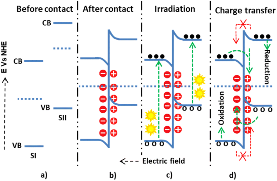 | ||
| Fig. 7 The possible S-scheme charge transfer mechanisms within semiconductor I and semiconductor II: (a and b) before-and-after contact; (c) during light irradiation and electron–hole generation; and (d) allowed and forbidden electron–hole migration. | ||
Jiang et al.83 developed the S-scheme mechanism within WO3 and ZnO heterojunctions. During contact, the electrons were transferred from ZnO with more negative potential to WO3 with less negative potential until the equilibrium stage, when band-bending and an interfacial internal electric field developed. During irradiation, the electrostatic attraction force drove the EHR from the less thermodynamic WO3 CB to ZnO VB. Thus, the electrons and holes with high thermodynamic energy on the WO3 and ZnO completed the reduction and oxidation reactions. The DMPO test showed that the DMPO–˙O2− signal in the EPR of ZnO was much greater than that of WO3, confirming the proposed S-scheme mechanism, indicating that the oxygen reduction reaction potential for WO3 is less efficient than that for ZnO. For this reason, the reduction redox reaction occurred on the ZnO, as proposed in the mechanism.
Jia et al.84 also proposed the S-scheme mechanism for ZnO/CdS/MoS2 heterojunction. The Mott–Schottky plots, Eg = EVB − ECB equation, and UV-vis-DRS were used to determine the material band edge potential. The CB potentials of MoS2, ZnO, and CdS were −0.37, −0.27, and −0.98 eV, respectively. The VB potentials of ZnO, MoS2, and CdS were calculated to be 2.68, 0.66, and 1.29 eV vs. NHE, respectively. ZnO, having a work function larger than Cd, migrates electrons from CdS to ZnO during contact, and within the interface, band bending and internal electric fields were developed. EPR tests were conducted in the presence of DMPO to detect ˙O2− and ˙OH free radicals, and the DMPO–˙OH EPR peak confirmed the potential of ZnO VB holes, which converted H2O to ˙OH radicals. This was impossible for the type II mechanism since the VB potential of CdS (1.29 eV) was more negative than the H2O oxidation potential to generate ˙OH radicals. Besides, the DMPO–˙O2− EPR peak confirmed the potential of CdS CB electrons converting O2 to ˙O2− radicals, which is also impossible for the type II mechanism since the CB potential of ZnO (−0.27 eV) was more positive than the reduction potential of O2 to ˙O2− radicals. In the study, MoS2 acted as an electron capture cocatalyst from the CB of CdS.
Park et al.7 also proposed the S-scheme mechanism between Cu2O and ZnO. UV-vis-DRS, XPS, and Mott–Schottky plots determined the semiconductors' band gap and flat band edges. The band gap obtained by UV-vis-DRS for Cu2O and ZnO was 1.9 and 3.2 eV, respectively, and the valence band maximum determined by XPS was 0.26 and 2.51 eV, respectively. The Mott–Schottky plots of ZnO and Cu2O had positive and negative slopes, respectively, indicating that they were n- and p-type semiconductors. The CB minimum potential energies were determined using the Eg = EVB − ECB equation, and the CB potentials for Cu2O and ZnO were −1.64 and −0.69 eV, respectively. To estimate whether type II or S-scheme mechanisms occurred, spin-trapping EPR analysis showed that the EPR DMPO–˙O2− signal intensity corresponding to ZnO was undetectable, while the DMPO–˙O2− signal for Cu2O was observed, which confirmed that oxygen reduction was much better on the CB of Cu2O than the CB of ZnO, unlike that of the type-II mechanism. Besides, the composite's EPR DMPO–˙O2− and DMPO–˙OH signals were strong, confirming the presence of charge transfer and synergistic effects. Thus, the S-scheme mechanism was the most possible mechanism between the n-type ZnO and p-type Cu2O junctions.
Conclusions
This mini-review summarizes critical ideas about doping and heterojunction that are interesting to a wide readership. Zinc oxide (ZnO) has a more negative conduction band (CB) potential than the reduction redox potential of O2/˙O2− (−0.33 V). Additionally, it has a more positive valence band (VB) potential than the oxidation redox potential of ˙OH/H2O (2.38 eV), meaning that oxygen and water can be easily reduced and oxidized to produce reactive oxygen species. However, ZnO has an electron–hole recombination problem. This issue can be solved through doping and heterojunction mechanisms, which improve charge transfer and extend visible light absorption properties (constituting 40% of the solar spectrum). Extrinsic doping creates a new mid-edge energy level associated with the host sp state and dopant 3d state, which forms a strong exchange interaction. On the other hand, heterojunctions improve electron–hole relaxation time without recombination. Unlike type II, the S- and Z-scheme heterojunctions can contribute electrons and holes with higher thermodynamic energy. However, electrons and holes present with low thermodynamic energy edge potential are lost by recombination and quenching. Including a noble metal mediator improves charge transfer and visible light-harvesting mechanisms. Sin-trapping electron paramagnetic resonance (EPR) analysis gives information on electron and hole transfer ways based on the DMPO–˙O2− or/and DMPO–˙OH signals.Further research is required to develop cost-effective, straightforward methods for industrial applications to create highly efficient, stable, and scalable light absorbers and proper charge transfer heterojunctions. Additionally, future investigations should focus on detailed characterization and control of semiconductor interfaces, electron–hole diffusion direction, and theoretical simulations for photocatalytic reaction feasibility.
Author contributions
Buzuayehu Abebe: conceptualization and writing – original draft; Neeraj K. Gupta writing – review & editing; Dereje Tsegaye: supervision and writing – review & editing.Conflicts of interest
There are no conflicts to declare.Acknowledgements
We acknowledge Adama Science and Technology University for financial support (ASTU/AS-R/052/2022).Notes and references
- S. Ali, P. M. Ismail, M. Khan, A. Dang, S. Ali, A. Zada, F. Raziq, I. Khan, M. S. Khan, M. Ateeq, W. Khan, S. H. Bakhtiar, H. Ali, X. Wu, M. I. A. Shah, A. Vinu, J. Yi, P. Xia and L. Qiao, Nanoscale, 2024, 16, 4352–4377 RSC.
- Y. Song, P. C. D. Mendes and S. M. Kozlov, J. Mater. Chem. A, 2023, 11, 13665–13676 RSC.
- D. Debnath, D. Sen, T. T. Neog, B. Saha and S. K. Ghosh, Cryst. Growth Des., 2024, 24, 871–885 CrossRef CAS.
- G. Thennarasu and A. Sivasamy, Powder Technol., 2013, 250, 1–12 CrossRef CAS.
- Y. Peng, S. Qin, W.-S. Wang and A.-W. Xu, CrystEngComm, 2013, 15, 6518 RSC.
- Y. Fu, Z. Ren, J. Wu, Y. Li, W. Liu, P. Li, L. Xing, J. Ma, H. Wang and X. Xue, Appl. Catal., B, 2021, 285, 119785 CrossRef CAS.
- B. H. Park, H. Park, T. Kim, S. J. Yoon, Y. Kim, N. Son and M. Kang, Int. J. Hydrogen Energy, 2021, 46, 38319–38335 CrossRef CAS.
- A. Das, M. Patra, M. Kumar P, M. Bhagavathiachari and R. G. Nair, Mater. Chem. Phys., 2021, 263, 124431 CrossRef CAS.
- M. Song, K. Qi, Y. Wen, X. Zhang, Y. Yuan, X. Xie and Z. Wang, Sci. Total Environ., 2021, 793, 148519 CrossRef CAS PubMed.
- S. A. Mahyoub, A. Hezam, F. A. Qaraah, K. Namratha, M. B. Nayan, Q. A. Drmosh, D. Ponnamma and K. Byrappa, ACS Appl. Energy Mater., 2021, 4, 3544–3554 CrossRef CAS.
- B. Abebe, D. Tsegaye and H. C. Ananda Murthy, RSC Adv., 2022, 12, 24374–24389 RSC.
- A. Mengistu, M. Naimuddin and B. Abebe, RSC Adv., 2023, 13, 24835–24845 RSC.
- A. K. M. Alsmadi, B. Salameh and M. Shatnawi, J. Phys. Chem. C, 2020, 124, 16116–16126 CrossRef CAS.
- A. I. Meky, M. A. Hassaan, H. A. Fetouh, A. M. Ismail and A. El Nemr, Sci. Rep., 2023, 13, 19329 CrossRef CAS.
- P. Rong, Y.-F. Jiang, Q. Wang, M. Gu, X.-L. Jiang and Q. Yu, J. Mater. Chem. A, 2022, 10, 6231–6241 RSC.
- A. Mclaren, T. Valdes-Solis, G. Li and S. C. Tsang, J. Am. Chem. Soc., 2009, 131, 12540–12541 CrossRef CAS.
- P. M. M. Gazzali, S. Rajan and G. Chandrasekaran, Ceram. Int., 2018, 44, 1566–1574 CrossRef CAS.
- S.-M. Lam, J.-C. Sin, A. Z. Abdullah and A. R. Mohamed, Desalin. Water Treat., 2012, 41, 131–169 CrossRef CAS.
- J. Meng, Z. Cui, X. Yang, S. Zhu, Z. Li, K. Qi, L. Zheng and Y. Liang, J. Catal., 2018, 365, 227–237 CrossRef CAS.
- Z. Wang, Y. Liu, B. Huang, Y. Dai, Z. Lou, G. Wang, X. Zhang and X. Qin, Phys. Chem. Chem. Phys., 2014, 16, 2758 RSC.
- P. Luo, F. Zhuge, Q. Zhang, Y. Chen, L. Lv, Y. Huang, H. Li and T. Zhai, Nanoscale Horiz., 2019, 4, 26–51 RSC.
- U. Wijesinghe, G. Longo and O. S. Hutter, Energy Adv., 2023, 2, 12–33 RSC.
- X. Chen, S. Shen, L. Guo and S. S. Mao, Chem. Rev., 2010, 110, 6503–6570 CrossRef CAS.
- F. Paquin, J. Rivnay, A. Salleo, N. Stingelin and C. Silva-Acuña, J. Mater. Chem. C, 2015, 3, 10715–10722 RSC.
- X. Wang, M. Sayed, O. Ruzimuradov, J. Zhang, Y. Fan, X. Li, X. Bai and J. Low, Appl. Mater. Today, 2022, 29, 101609 CrossRef.
- F. He, B. Zhu, B. Cheng, J. Yu, W. Ho and W. Macyk, Appl. Catal., B, 2020, 272, 119006 CrossRef CAS.
- F. Xu, K. Meng, B. Cheng, S. Wang, J. Xu and J. Yu, Nat. Commun., 2020, 11, 4613 CrossRef CAS PubMed.
- P. Xia, S. Cao, B. Zhu, M. Liu, M. Shi, J. Yu and Y. Zhang, Angew. Chem., Int. Ed., 2020, 59, 5218–5225 CrossRef CAS PubMed.
- A. A. Azab, E. E. Ateia and S. A. Esmail, Appl. Phys. A: Mater. Sci. Process., 2018, 124, 469 CrossRef.
- Y. Yang, Y. Li, L. Zhu, H. He, L. Hu, J. Huang, F. Hu, B. He and Z. Ye, Nanoscale, 2013, 5, 10461 RSC.
- C. Klingshirn, J. Fallert, H. Zhou, J. Sartor, C. Thiele, F. Maier-Flaig, D. Schneider and H. Kalt, Phys. Status Solidi, 2010, 247, 1424–1447 CrossRef CAS.
- D. E. Aimouch, S. Meskine, A. Boukortt and A. Zaoui, J. Magn. Magn. Mater., 2018, 451, 70–78 CrossRef CAS.
- K. C. Barick, S. Singh, M. Aslam and D. Bahadur, Microporous Mesoporous Mater., 2010, 134, 195–202 CrossRef CAS.
- B. D. Yuhas, D. O. Zitoun, P. J. Pauzauskie, R. He and P. Yang, Angew. Chem., Int. Ed., 2006, 45, 420–423 CrossRef CAS PubMed.
- Y. Wang, Y. Yang, X. Zhang, X. Liu and A. Nakamura, CrystEngComm, 2012, 14, 240–245 RSC.
- M. Pashchanka, R. C. Hoffmann, A. Gurlo, J. C. Swarbrick, J. Khanderi, J. Engstler, A. Issanin and J. J. Schneider, Dalton Trans., 2011, 40, 4307 RSC.
- R. Ponnusamy, S. C. Selvaraj, M. Ramachandran, P. Murugan, P. M. G. Nambissan and D. Sivasubramanian, Cryst. Growth Des., 2016, 16, 3656–3668 CrossRef CAS.
- Z. Wang, J. Xue, D. Han and F. Gu, ACS Appl. Mater. Interfaces, 2015, 7, 308–317 CrossRef CAS.
- A. Albert Manoharan, R. Chandramohan, K. D. Arun Kumar, S. Valanarasu, V. Ganesh, M. Shkir, H. Algarni and S. AlFaify, J. Mater. Sci.: Mater. Electron., 2018, 29, 13077–13086 CrossRef CAS.
- K. Niranjan, S. Dutta, S. Varghese, A. K. Ray and H. C. Barshilia, Appl. Phys. A: Mater. Sci. Process., 2017, 123, 250 CrossRef.
- M. A. Garcia, J. M. Merino, E. Fernández Pinel, A. Quesada, J. de la Venta, M. L. Ruíz González, G. R. Castro, P. Crespo, J. Llopis, J. M. González-Calbet and A. Hernando, Nano Lett., 2007, 7, 1489–1494 CrossRef CAS.
- J. M. D. Coey, P. Stamenov, R. D. Gunning, M. Venkatesan and K. Paul, New J. Phys., 2010, 12, 053025 CrossRef.
- T. Mizik, Agronomy, 2021, 11, 1096 CrossRef.
- P. Jakes and E. Erdem, Phys. Status Solidi RRL, 2011, 5, 56–58 CrossRef CAS.
- R. Khalid, A. N. Alhazaa and M. A. M. Khan, Appl. Phys. A: Mater. Sci. Process., 2018, 124, 536 CrossRef.
- M. Ahmad, E. Ahmed, W. Ahmed, A. Elhissi, Z. L. Hong and N. R. Khalid, Ceram. Int., 2014, 40, 10085–10097 CrossRef CAS.
- P. Sharma, A. Gupta, K. V. Rao, F. J. Owens, R. Sharma, R. Ahuja, J. M. O. Guillen, B. Johansson and G. A. Gehring, Nat. Mater., 2003, 2, 673–677 CrossRef CAS.
- N. Ali, B. Singh, V. A. R. Vijaya, S. Lal, C. S. Yadav, K. Tarafder and S. Ghosh, J. Phys. Chem. C, 2021, 125, 7734–7745 CrossRef CAS.
- I. Djerdj, G. Garnweitner, D. Arčon, M. Pregelj, Z. Jagličić and M. Niederberger, J. Mater. Chem., 2008, 18, 5208 RSC.
- P. S. Vindhya, S. Suresh, R. Kunjikannan and V. T. Kavitha, J. Environ. Health Sci. Eng., 2023, 21, 167–185 CrossRef CAS.
- Z. Chen, Y. Fang, L. Wang, X. Chen, W. Lin and X. Wang, Appl. Catal., B, 2021, 296, 120369 CrossRef CAS.
- K. Chehhat, A. Mecif, A. H. Mahdjoub, R. Nazir, M. A. Pandit, F. Salhi and A. Noua, J. Sol-Gel Sci. Technol., 2023, 106, 85–94 CrossRef CAS.
- A. Kaphle, E. Echeverria, D. N. Mcllroy, K. Roberts and P. Hari, J. Nanosci. Nanotechnol., 2019, 19, 3893–3904 CrossRef CAS PubMed.
- A. Chanda, S. Gupta, M. Vasundhara, S. R. Joshi, G. R. Mutta and J. Singh, RSC Adv., 2017, 7, 50527–50536 RSC.
- J. Kazmi, P. C. Ooi, S. R. A. Raza, B. T. Goh, S. S. A. Karim, M. H. Samat, M. K. Lee, M. F. Mohd Razip Wee, M. F. M. Taib and M. A. Mohamed, J. Alloys Compd., 2021, 872, 159741 CrossRef CAS.
- B. Salameh, A. M. Alsmadi and M. Shatnawi, J. Alloys Compd., 2020, 835, 155287 CrossRef CAS.
- A. Iribarren, E. Hernández-Rodríguez and L. Maqueira, Mater. Res. Bull., 2014, 60, 376–381 CrossRef CAS.
- J. H. Zheng, J. L. Song, Q. Jiang and J. S. Lian, J. Mater. Sci.: Mater. Electron., 2012, 23, 1521–1526 CrossRef CAS.
- Y. Tian, Y. Li, M. He, I. A. Putra, H. Peng, B. Yao, S. A. Cheong and T. Wu, Appl. Phys. Lett., 2011, 98, 2009–2012 Search PubMed.
- A. Khalid, P. Ahmad, A. I. Alharthi, S. Muhammad, M. U. Khandaker, M. Rehman, M. R. I. Faruque, I. U. Din, M. A. Alotaibi, K. Alzimami and D. A. Bradley, Nanomaterials, 2021, 11, 451 CrossRef CAS PubMed.
- B. Abebe and H. C. A. Murthy, RSC Adv., 2022, 12, 5816–5833 RSC.
- B. Divband, M. Khatamian, G. R. K. Eslamian and M. Darbandi, Appl. Surf. Sci., 2013, 284, 80–86 CrossRef CAS.
- T. N. Q. Trang, T. B. Phan, N. D. Nam and V. T. H. Thu, ACS Appl. Mater. Interfaces, 2020, 12, 12195–12206 CrossRef CAS.
- S. Wang, F. Jia, X. Wang, L. Hu, Y. Sun, G. Yin, T. Zhou, Z. Feng, P. Kumar and B. Liu, ACS Omega, 2020, 5, 5209–5218 CrossRef CAS.
- S. Chakma and V. S. Moholkar, Ultrason. Sonochem., 2015, 22, 287–299 CrossRef CAS PubMed.
- C. P. Rajan, N. Abharana, S. N. Jha, D. Bhattacharyya and T. T. John, J. Phys. Chem. C, 2021, 125, 13523–13533 CrossRef CAS.
- Z. Zhang, L. Bai, Z. Li, Y. Qu and L. Jing, J. Mater. Chem. A, 2019, 7, 10879–10897 RSC.
- J. Ran, M. Jaroniec and S. Qiao, Adv. Mater., 2018, 30, 1–31 Search PubMed.
- J. Low, J. Yu, M. Jaroniec, S. Wageh and A. A. Al-Ghamdi, Adv. Mater., 2017, 29, 1601694 CrossRef.
- H. Yang, Mater. Res. Bull., 2021, 142, 111406 CrossRef CAS.
- L.-Y. Zhang, J.-J. Yang and Y.-H. You, RSC Adv., 2021, 11, 38654–38666 RSC.
- H. Park, N. Son, B. H. Park, C. Liu, S. W. Joo and M. Kang, Chem. Eng. J., 2022, 430, 133104 CrossRef CAS.
- H. S. Moon, K. Hsiao, M. Wu, Y. Yun, Y. Hsu and K. Yong, Adv. Mater., 2023, 35, 1–11 Search PubMed.
- T. Di, Q. Xu, W. Ho, H. Tang, Q. Xiang and J. Yu, ChemCatChem, 2019, 11, 1394–1411 CrossRef CAS.
- T. Zhou, J. Wang, S. Chen, J. Bai, J. Li, Y. Zhang, L. Li, L. Xia, M. Rahim, Q. Xu and B. Zhou, Appl. Catal., B, 2020, 267, 118599 CrossRef CAS.
- S. Ruan, W. Huang, M. Zhao, H. Song and Z. Gao, Mater. Sci. Semicond. Process., 2020, 107, 104835 CrossRef CAS.
- W. Ali, Z. Li, L. Bai, M. Z. Ansar, A. Zada, Y. Qu, S. Shaheen and L. Jing, Catalysts, 2023, 13, 696 CrossRef CAS.
- X. Liu, A. Dang, T. Li, Y. Sun, T.-C. Lee, W. Deng, S. Wu, A. Zada, T. Zhao and H. Li, ACS Sens., 2023, 8, 1287–1298 CrossRef CAS PubMed.
- H. Wang, L. Zhang, Z. Chen, J. Hu, S. Li, Z. Wang, J. Liu and X. Wang, Chem. Soc. Rev., 2014, 43, 5234 RSC.
- K. Xu, Z. Liu, S. Qi, Z. Yin, S. Deng, M. Zhang and Z. Sun, RSC Adv., 2020, 10, 34702–34711 RSC.
- C. Cheng, B. He, J. Fan, B. Cheng, S. Cao and J. Yu, Adv. Mater., 2021, 33, 1–8 Search PubMed.
- X. Xu, J. Wang and Y. Shen, Langmuir, 2021, 37, 7254–7263 CrossRef CAS PubMed.
- Z. Jiang, B. Cheng, Y. Zhang, S. Wageh, A. A. Al-Ghamdi, J. Yu and L. Wang, J. Mater. Sci. Technol., 2022, 124, 193–201 CrossRef CAS.
- Y. Jia, Z. Wang, X.-Q. Qiao, L. Huang, S. Gan, D. Hou, J. Zhao, C. Sun and D.-S. Li, Chem. Eng. J., 2021, 424, 130368 CrossRef CAS.
| This journal is © The Royal Society of Chemistry 2024 |