
 Open Access Article
 This Open Access Article is licensed under a Creative Commons Attribution-Non Commercial 3.0 Unported Licence
Sodium chloride-assisted CVD enables controlled synthesis of large single-layered MoS2†
Ting Liab,
Chong Zhangac,
Yali Caiac,
Wenfeng Yuead,
Jie Liua,
Chuanwei Huangb,
Quansheng Guoc,
Tingting Jia *ac and
Shuhui Yua
*ac and
Shuhui Yua
aShenzhen Institute of Advanced Electronic Materials, Shenzhen Institute of Advanced Technology, Chinese Academy of Sciences, Shenzhen 518055, China
bSchool of Materials Science and Engineering, Shenzhen University, Shenzhen 518055, China
cSchool of Materials Science and Engineering, Hubei University, Wuhan 430062, China. E-mail: jia.tingting@hubu.edu.cn
dSchool of Instrumentation Science and Engineering, Harbin Institute of Technology, Harbin 150001, China
First published on 30th September 2024
Abstract
Thin-layer MoS2 has attracted much interest because of its potential in diverse technologies, including electronics, optoelectronics and catalysis these few years. In particular, finding a simple and effective solution for large-scale growth of thin-layer semiconductor nanosheets is a prerequisite for achieving their excellent performance. In this paper, we investigated four different substrates under identical conditions for MoS2 film growth and observed a strong correlation between substrate surface conditions and MoS2 growth. To enhance substrate performance, a low-concentration NaCl water solution (25 mg mL−1) was employed for pre-treating the substrate surface, thereby modifying its initial state. In the chemical vapor deposition (CVD) growth environment, the introduced halide ions served as surface dangling bonds. The pre-treated led to a remarkable 90% increase in the growth rate of MoS2 on the substrate surface, facilitating the production of large monolayer MoS2 sheets (∼200 μm). This growth mechanism further enabled the manufacturing of ultra-large single crystals (∼1 mm). Consequently, our research presents a straightforward and cost-effective approach for the large-scale production of nanosheets. Field-effect transistors (FETs) based on the pre-treated monolayer MoS2 exhibited high mobility (12 cm2 V−1 s−1) and a large on/off ratio (104). Therefore, our research provides a simple and low-cost approach for large-scale production of nanosheets for use in high-quality electronics over large areas.
1. Introduction
In recent years, thin-layer transition metal dichalcogenides have attracted much attention due to their excellent and unique electrical, thermal, mechanical, and optical properties, making them desirable candidate materials in compact, lightweight, integrated electronic systems.1,2 More obviously, among these materials, thin-layer MoS2 has been highly favored because of its excellent properties. Firstly, the thin-layer MoS2 possessed ideal properties as channel materials for high-performance optoelectronic and electronic devices due to the fantastic 2D restriction of electrons character.3,4 Secondly, MoS2 owns admirable flexibility, mechanical strength, and optical transparency properties, which is crucial for devices with special requirements for transparency and flexibility.5,6 Based on this, efforts have been made to directly synthesize large-size or large-domain MoS2 single crystals with good crystal quality, low defect density, and controlled layer thickness.7 Plenteous studies have been committed to the preparation of thin-layer MoS2,8–12 Overall, the chemical vapor deposition (CVD) technique, with outstanding controllability and scalability, has shown significant potential in producing high-quality TMD (Transition Metal Dichalcogenide) monolayers.13,14At far, some effective strategies to conducting epitaxial growth large-size, high-quality films. One of the key methods is altering the substrate type or modifying the surface state of the substrate in order to modify the conditions for epitaxial growth. In the past research, a variety of substrates have been selected for the preparation of MoS2 thin films by CVD,6,15–19 and the surface properties of different substrates are also different, which may affect not only the number, shape and size of MoS2, but also the properties of MoS2 grown, and then affect the performance of the devices.
Numerous studies have demonstrated the important role that alkali metal salts20–23 play in controlling the development of 2D TMDs and their superior performance.21,24,25 Li et al.24 recently proposed a gas–liquid–solid (VLS) reaction to prepare high-quality MoS2 nanoribbons on a sodium chloride (NaCl) single crystal. NaCl and MoO3 form a eutectic compound (Na2Mo2O7) with a relatively low melting point. Sulfur vapor rapidly dissolves into the liquid and reacts on the NaCl surface to form solid monolayer MoS2. Chang et al.25 introduced a self-capping VLS (SCVLS) reaction for growing large single crystals. A solid precursor (Na2Mo2O7), composed of a eutectic reaction between MoO3 and NaF layers at high temperatures, is sulfurized to form MoS2 seeds. As the liquid advances along the growth direction, plate-like MoS2 with sizes up to 200 μm can be achieved. These methods utilize similar principles to prepare large-sized MoS2, but the introduction a large amount of Na+ may have some potential negative effects. To obtain a highly uniform and successful promotion of thin-layer MoS2 films development, it is still a significant issue to improve the surface state of the substrate and assist the growth of thin-layer MoS2 films with the lowest amount of impurities introduced, and this requires more thorough and in-depth study.
This paper presents a pre-treatment mechanism for growing large single crystals and fully covered few-layer MoS2 films. Four different substrates were examined for growing MoS2 films under the same conditions, and it was found that the surface condition of the substrate strongly influences the growth of MoS2. A low concentration NaCl water solution (25 mg mL−1) was introduced to pre-treat the substrate surface and alter the substrate initial state. In the CVD growth environment, the introduced halide ions act as surface dangling bonds. The growth rate of MoS2 on the substrate surface increased by approximately 90% after pre-treatment, enabling the growth of large monolayer MoS2 (∼200 μm). This growth mechanism makes it possible to manufacture ultra-large single crystals (∼1 mm). Meanwhile, the quality and uniformity of the MoS2 grown using this method were evaluated. Furthermore, field-effect transistors (FETs) based on the pre-treated monolayer MoS2 exhibited high mobility (12 cm2 V−1 s−1) and a large on/off ratio (104). These research findings are significant for promoting the large-scale, low-cost industrial growth of high-quality few-layer MoS2.
2. Experimental section
2.1 Sample preparation and pre-treat of substrate
The schematic illustration for the experimental set-up used chemical vapor deposition (CVD) to synthesize MoS2 is shown in Fig. 1a. We used MoO3 powder (>99.5%, Sigma Aldrich) and sulfur powder (S) (>99%, Sigma Aldrich) as precursors. The tube furnace equipped with dual temperature zones was used, the MoO3 powder (10 mg) in the upstream zone and S powder (350 mg) in the downstream area were placed in the two quartz boats, and the distance of the boat was 18 cm. Four different substrates (Si, sapphire, SiO2/Si, mica) were selected to grow MoS2. Before the experiment, the substrate was ultrasonic cleaned with acetone, absolute ethanol, and deionized water for 5 min respectively. The substrate was placed in the downstream temperature zone supported by quartz pads and was divided into two placement modes: parallel (facedown) and perpendicular (upright) to the direction of airflow.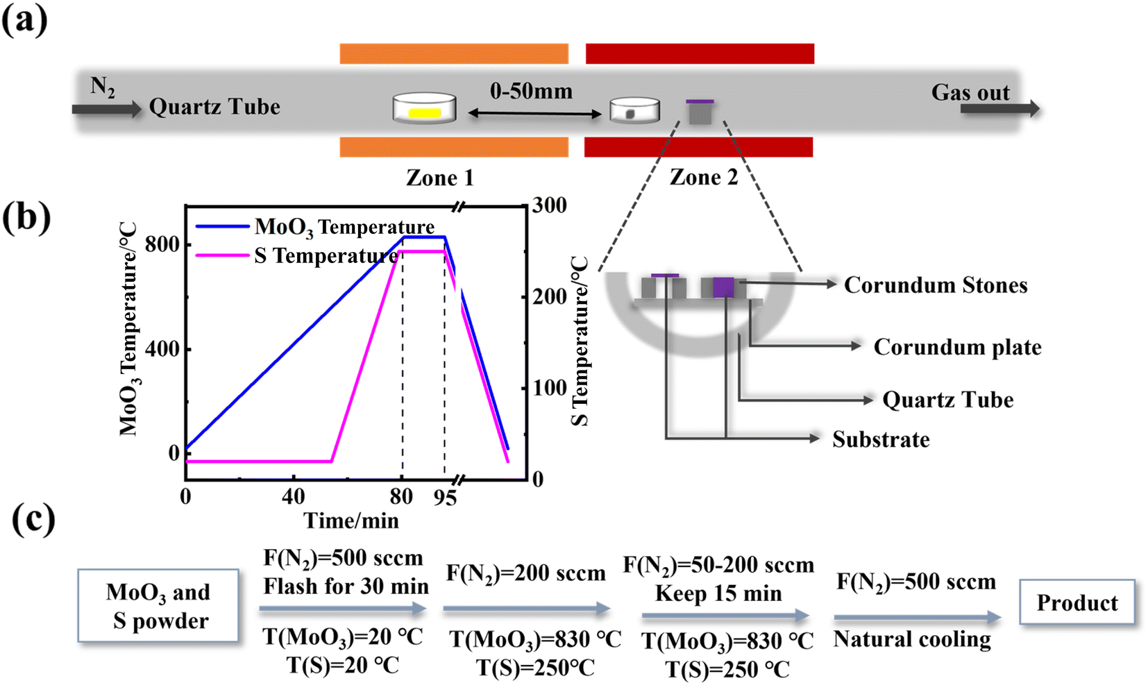 | ||
| Fig. 1 (a) Schematic illustration for the experimental set-up, (b) temperature vs. time profile for MoS2 growth, (c) setting of growth system temperature and carrier gas flow rate. | ||
The aqueous solution of NaCl (25 mg mL−1) was prepared in advance, 0.5 mL was dropped onto the substrate surface, spun coated with a homogenizer at a rate of 800 rpm for 30 s, and then placed on the surface of the heating table preheated at 120 °C, dried for 2 min and cooled naturally. The pretreated substrate is placed in a tube furnace for subsequent CVD growth.
2.2 Growth of MoS2
In our experiments, quartz boats containing S powder and MoO3 powder were positioned at the upstream and downstream ends of the N2 flow, respectively, with a mass ratio of 3![[thin space (1/6-em)]](https://www.rsc.org/images/entities/char_2009.gif) :1 and a separation distance of 18 cm. The heating procedure is shown in Fig. 1b. MoO3 rises to 830 °C with a heating rate of 10 °C min−1. At the same time, the S powder is kept at room temperature for 53 min, and then heated to 250 °C with 10 °C min−1, reacting at 830 °C for 10–20 min, The substrate is placed in the downstream temperature zone supported by quartz pads and the placement is perpendicular (upright) to the direction of N2 flow, we found that the optimum N2 flow rates and placement distance are around 200 sccm and 20 mm, respectively. Then the CVD system begins to cool naturally, and the growth ends. The setting procedure of temperature and carrier gas flow rate is shown in Fig. 1c.
:1 and a separation distance of 18 cm. The heating procedure is shown in Fig. 1b. MoO3 rises to 830 °C with a heating rate of 10 °C min−1. At the same time, the S powder is kept at room temperature for 53 min, and then heated to 250 °C with 10 °C min−1, reacting at 830 °C for 10–20 min, The substrate is placed in the downstream temperature zone supported by quartz pads and the placement is perpendicular (upright) to the direction of N2 flow, we found that the optimum N2 flow rates and placement distance are around 200 sccm and 20 mm, respectively. Then the CVD system begins to cool naturally, and the growth ends. The setting procedure of temperature and carrier gas flow rate is shown in Fig. 1c.
We first explored the specific parameters that affect thin film growth, including carrier gas flow rate, distance between molybdenum-substrate placement, and substrate placement method, as shown in Fig. S1.†
2.3 Device fabrication and characterization
The 3D confocal laser microscope (VK-X1000, Beijing Chuang Cheng Zhi Jia Technology Co., Ltd, China) and Scanning Electron Microscope (SEM, Apreo 2, Thermo Fisher Scientific, America) were used to observe the morphology of MoS2 and the distribution of element was tested by Energy Dispersive Spectroscopy (EDS). Photoluminescence (PL) and Raman characterizations were performed by Raman spectroscopy, and the Raman spectroscopy with irradiation using an Ar ion laser beam at 532 nm and a high-resolution dispersive Raman spectrometer (Aramis; Horiba Jobin Yvon, France). In addition, the micro-morphology of the MoS2 nanosheets was measured by Atomic Force Microscope (AFM, Cypher S, Oxford Instruments, UK). Transmission electron microscopy (TEM, JEM-F200, JEOL Ltd, Japan) with spatially resolved energy dispersive X-ray analysis was used to determine the lattice parameters and element composition of MoS2. The electrical characteristics of field-effect transistors were tested using semiconductor analyzer (Keithley 4200A-SCS device, Tektronix, America). In this experiment, FETs were fabricated with a p-type silicon-based semiconductor as the back gate, a gate oxide layer of SiO2 with a thickness of 100 nm, and the channel material being the prepared MoS2 thin film sample. The sample was spin-coated with photoresist PMMA (200 nm), followed by heating at 180 °C for 120 s. Electron beam exposure was used to pattern the electrode, followed by development, fixation, removal of residual chemicals. Finally, the photoresist was removed by immersing the sample in acetone solution at 55 °C for 30 min, followed by 10 min of ultrasonic treatment and drying with nitrogen gas.3. Results and discussion
After exploring the best growth conditions (Fig. S1†), the experimental growth parameters of N2 flow rate is fixed as 200 sccm (standard cubic centimeter per minute), and the distance between MoO3 and substrate is 20 mm to ensure that the growth conditions are exactly the same. We further explore the influence of the substrate. The morphology, Raman and PL spectrums of MoS2 nanosheet growth on mica, c-plane sapphire, SiO2/Si and Si substrate are studied detail, and the results are shown in Fig. 2. | ||
| Fig. 2 (a) Optical microscopy images, (b) Raman spectrums and (c) PL spectrums of MoS2 nanosheet growth on mica, c-plane sapphire, SiO2/Si, and Si substrate. | ||
As shown in Fig. 2a, the MoS2 nanosheet has a high-density overlap on mica, and the size of a single MoS2 is about 10 μm. The MoS2 grown on SiO2/Si has a single domain size of about 50–70 μm and has a regular triangular morphology (Fig. 2b), and the nucleation point is a bright white triangle in the middle of the MoS2. MoS2 is growing extremely uniformly on the sapphire substrate, single domain size can reach 159 μm, its single domains are joined to one another to form flakes, and their combined size can reach a millimeter level (Fig. S2†). In contrast, the morphology of MoS2 grown on SiO2/Si shows many kinds, such as dendritic, triangular, and butterfly shapes, and its distribution is also irregular (Fig. S3†).
The Raman spectrum of MoS2 grown on sapphire substrate shows characteristic E2g1 and A1g peaks at 384.6 cm−1 and 403.5 cm−1 with a peak separation of 18.9 cm−1 (Fig. 2c). The MoS2 nanosheet also exhibited characteristic excitonic photoluminescence (PL) peaks at 605 nm and 675 nm (Fig. 2c), These features are in good agreement with the monolayer MoS2 in the literature,6,7 indicating prepared MoS2 has excellent crystallinity, and also with the height data (0.7 nm) of the monolayer MoS2 nanosheet measured in AFM (Fig. S4†). The Raman characteristic peak frequency difference of MoS2 grown on mica, SiO2/Si and Si substrate is about 21.5 cm−1, 20.3 cm−1, and 19 cm−1, respectively.26 The results are consistent with the height data in Fig. S4,† indicating that the MoS2 grown on the test sites of mica, SiO2/Si and Si substrates are triple-layer, double-layer and single-layer, respectively.
The surfaces of MoS2 nanosheets grown on mica substrate surfaces are smooth, the interlayer height is visible, and the red shift of the A exciton peak was observed in Fig. 3c, this may driven by applying tensile strain on MoS2 (ref. 27 and 28) The size and shape of MoS2 nanosheets own huge differences when grown on different substrates under the same growth environment due to the difference in adsorption energy and diffusion barrier on the substrate surface,29–31 The adsorption energy and diffusion barrier of c-plane sapphire surface are higher compare with other substrates in this paper,32,33 which lead to the time of precursors adsorption is longer and the diffusion distance is shorter than other substrates, so the growth rate of MoS2 flakes on the sapphire surface becomes easier to form monolayer structure. Silicon is a crucial substrate for the production of field effect transistors, however, the growth conditions on the two silicon substrates are unfavorable. It is vital to find a solution for how to enhance MoS2 development on silicon substrates and achieve the creation of large-area monolayer MoS2.
 | ||
| Fig. 3 (a, b and c) The SEM images of MoS2 nanosheet on Si substrates with NaCl solution pretreated and non-pretreated area, scale bars in (a–c), 100 μm. (d) Laser confocal microscope images of MoS2 grown on sapphire substrates with NaCl solution pretreated, (e)AFM image of the shown in the dashed black box in (d), (f) the corresponding height profile along the red line in the AFM image. (g) Raman, (h) PL and (i) schematic diagram of the operation of NaCl solution pretreated substrate surface. | ||
To prepare large-size and high-quality monolayer MoS2 in CVD technology, the pretreatment of substrate is important. The pretreatment boundary has been marked with red lines (Fig. 5b and c), the schematic diagram of the pretreatment of Si substrate with NaCl solution is shown in Fig. 3i. After pre-treating, MoS2 growth on the Si substrate surface has been remarkably improved, the size of a single domain rises, and the interdomain connection achieves huge area expansion. After increasing the concentration of NaCl solution by 5 times, the promotion effect of this growth can be observed more clearly on the substrate surface (Fig. S4†). However, this high concentration also brings significant impurity contamination, which affects the use of 2D materials. At the same time, we also explored the use of low-concentration NaCl solution for the pre-treatment of sapphire substrates (Fig. 3d–f). After pre-treatment, the single domain size can reach the millimeter scale (∼1 mm) (Fig. S5†). Meanwhile, we also observed a similar vapor–liquid–solid (VLS) growth24,25,34 processes during our growth process, and we conducted EDS analysis on the black dot-like substances in the middle (Fig. S6 and Table S1†). During the high-temperature reaction process, S and MoO3 also vaporize under elevated temperatures and mix with the inert nitrogen gas. NaCl forms a liquid phase on the substrate surface. Cl− from NaCl interacts with Mox+ precursors through chemical adsorption, while S vapor also forms a liquid-phase mixture with the liquid NaCl.23,35 This facilitates effective contact and reaction between the two precursors on the substrate surface.36,37 Simultaneously, Na+ and chloride ions Cl− alter the surface potential of the substrate, inducing the attachment of precursors to the substrate surface. The reaction proceeds continuously, and with the movement of the liquid phase, MoS2 grows uniformly on the substrate surface. The reaction ceases once the temperature decreases.
 | ||
| Fig. 4 On the Si substrate surface pre-treated with a NaCl solution, the laser confocal microscope images of MoS2 at different growth times are shown in (a–e); (b) introducing a small amount of Na+ and Cl− on the clean Si substrate surface (c), when the preset growth temperature is reached, small MoS2 molecules attach to these ion suspension bonds (d) and further grow large (e). | ||
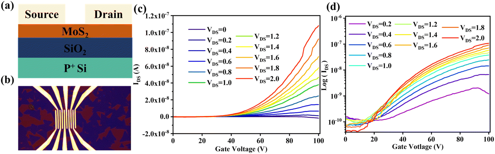 | ||
| Fig. 5 (a) Cross-sectional schematic diagram of FET. (b) Optical image of FET based on monolayer MoS2. (c) The transfer characteristic curve of the FET. (d) The output the characteristic curve of the FET. | ||
Trace amounts of Na element, as well as a large amount of S and Mo elements, can be observed. AFM morphology analysis and height scans were performed on selected areas (Fig. 3e and f), revealing a height of approximately 0.7 nm, which matches well with the thickness of a monolayer of MoS2. To determine whether the electronic structure of the grown MoS2 is affected by the substrate pre-treatment, we conducted Raman (Fig. 3g) and PL (Fig. 3h) measurements. The results indicate that the material structure is hardly affected by the two different growth environments. Due to the presence of specific interactions in this hybrid structure, we observed some interesting phenomena, such as enhanced PL intensity and slight shifts in Raman peaks. Detailed studies on this aspect are still ongoing and are expected to be presented in future reports. A method has proved the variation of Raman peak positions with temperature for CVD-grown MoS2, revealing that the temperature dependence of the thermal and anharmonic properties of TMDCs can affect the Raman characteristic peak positions.38 This information can be utilized to assist in the description of performance variations in two-dimensional materials. As shown in Fig. 3i, the pre-treatment process we used is simple and easy to scale up.
We observed a series of changes on the substrate surface under the same pre-treatment and growth conditions at different reaction times, as shown in Fig. 4a. At the pre-treatment interface, a distinct “growth line” composed of light purple fluffy and filamentous substances can be observed (Fig. 4a), the growth coverage at the pre-treatment boundary can reach approximately 90%. A significant amount of filamentous material can be observed within the pre-treatment interface, with a white bright spot at the interface between the filamentous material and the substrate. As the growth continues, the filamentous material disappears, and the white bright spot laterally grows larger (Fig. 4c), until multiple regions combine and the reaction reaches its completion (Fig. 4d). Based on the observed growth changes, we have summarized a growth mechanism in Fig. 4b–e, corresponding to different stages in Fig. 4a. Low concentrations of Na+ and Cl− are introduced to the substrate surface, acting as dangling bonds (Fig. 4b and c). When S and MoO3 vapors reach the reaction zone, the dangling bonds on the substrate surface can timely anchor the precursor reactants and facilitate the occurrence of MoS2 reaction (Fig. 4d and e), altering the surface potential and making it easier for the precursor atmosphere to adhere to the substrate surface. The edge diffusion-assisted growth led by cornered catalyst particles was triggered, promoting the lateral growth of monocrystalline MoS2. In previous research, it has been documented that the chemical vapor deposition (CVD) process for growing monolayer MoS2 can be enhanced by the intrinsic doping effects occurring spontaneously in alkali metal compounds.39,40 In summary, the introduction of halogen ions has two advantageous effects on the entire process: (1) it increases the connection between the substrate and the precursor reactants, (2) it increases the nucleation sites on the substrate surface and enlarges the growth coverage area. To verify whether the introduction of halogen ions affects MoS2, we performed cross-sectional TEM, EDS, and XRD analysis on MoS2 grown on a sapphire substrate (Fig. S6†). TEM confirmed that we observed the (002) crystal plane, which is consistent with the XRD data. At the same time, no halogen ions were found at multiple locations, which could be due to the removal of ions during sample preparation. Furthermore, it also indicates that low doping has minimal influence on the MoS2 sample. The experimental findings demonstrate that the fabricated MoS2 film exhibits uniformity and high-quality, single-crystal characteristics, making it suitable for subsequent investigation and production of MoS2 field-effect transistors.
The conductive channel in the MoS2 back-gate field-effect transistor (FET) is formed by the accumulation of charge carriers. As the applied gate voltage VGS increases, the electron concentration in the MoS2 channel gradually increases, leading to transistor channel conduction. We use the following formula to calculate the field-effect mobility (μFE),41

4. Conclusions
In summary, a simple and low-cost CVD method for growing thin-layers MoS2 is proposed, which is compatible with the integrated circuit device manufacturing process and is expected to be applied to the growth of waferscale MoS2 thin films. Four different substrates were examined for growing MoS2 and found that the surface condition of the substrate strongly influences the growth of MoS2. A low-concentration NaCl water solution (25 mg mL−1) was introduced to pre-treat the substrate surface and alter the substrate's initial state, the introduced halide ions act as surface dangling bonds. The growth rate of MoS2 on the substrate surface increased by approximately 90% after pre-treatment, enabling the growth of large monolayer MoS2 (∼200 μm). This growth mechanism makes it possible to manufacture ultra-large single crystals (∼1 mm). Besides, the FET based on monolayer MoS2 exhibits the mobility of 12 cm2 V−1 S−1, and the on/off current ratio of ∼104. In summary, this study systematically investigates some interesting methods that provide insights into the growth of high-quality monolayer MoS2. It is of significant importance for promoting large-scale, low-cost industrial production of high-quality monolayer MoS2.Data availability
The data that support the findings of this study are available from the corresponding author (Tingting Jia), upon reasonable request.Conflicts of interest
There are no conflicts to declare.Acknowledgements
This work was financially supported by the National Natural Science Foundation of China (51702351), and the Basic and Applied Basic Research Foundation of Guangdong Province (2020B1515120019).References
- L. Huang, A. Krasnok, A. Alu, Y. Yu, D. Neshev and A. E. Miroshnichenko, Rep. Prog. Phys., 2022, 85, 046401 CrossRef CAS PubMed.
- S. B. Mitta, M. S. Choi, A. Nipane, F. Ali, C. Kim, J. T. Teherani, J. Hone and W. J. Yoo, 2D Materials, 2020, 8, 012002 CrossRef.
- N. Li, Q. Wang, C. Shen, Z. Wei, H. Yu, J. Zhao, X. Lu, G. Wang, C. He, L. Xie, J. Zhu, L. Du, R. Yang, D. Shi and G. Zhang, Nat. Electron., 2020, 3, 711–717 CrossRef CAS.
- C.-H. Yang, Y.-F. Chung, Y.-S. Su, K.-T. Chen, Y.-S. Huang and S.-T. Chang, J. Comput. Electron., 2022, 21, 571–581 CrossRef CAS.
- M. Park, Y. J. Park, X. Chen, Y.-K. Park, M.-S. Kim and J.-H. Ahn, Adv. Mater., 2016, 28, 2555 CrossRef CAS.
- W. Li, M. Xu, J. Gao, X. Zhang, H. Huang, R. Zhao, X. Zhu, Y. Yang, L. Luo, M. Chen, H. Ji, L. Zheng, X. Wang and W. Huang, Adv. Mater., 2022, 35(8), 2207447 CrossRef PubMed.
- Y. Zhang, Y. Yao, M. G. Sendeku, L. Yin, X. Zhan, F. Wang, Z. Wang and J. He, Adv. Mater., 2019, 31(41), 1901694 CrossRef CAS PubMed.
- H. S. Matte, A. Gomathi, A. K. Manna, D. J. Late, R. Datta, S. K. Pati and C. N. Rao, Angew Chem. Int. Ed. Engl., 2010, 49, 4059–4062 CrossRef CAS PubMed.
- Z. Zeng, Z. Yin, X. Huang, H. Li, Q. He, G. Lu, F. Boey and H. Zhang, Angew Chem. Int. Ed. Engl., 2011, 50, 11093–11097 CrossRef CAS PubMed.
- G. Eda, H. Yamaguchi, D. Voiry, T. Fujita, M. Chen and M. Chhowalla, Nano Lett., 2011, 11, 5111–5116 CrossRef CAS PubMed.
- S. Helveg, J. V. Lauritsen, E. Laegsgaard, I. I. Stensgaard, J. K. Norskov, B. S. Clausen, H. Topsoe and F. Besenbacher, Phys. Rev. Lett., 2000, 84, 951–954 CrossRef CAS PubMed.
- K. G. Zhou, N. N. Mao, H. X. Wang, Y. Peng and H. L. Zhang, Angew Chem. Int. Ed. Engl., 2011, 50, 10839–10842 CrossRef CAS PubMed.
- X. Chen, Y. J. Park, T. Das, H. Jang, J. B. Lee and J. H. Ahn, Nanoscale, 2016, 8, 15181–15188 RSC.
- K. Kang, S. Xie, L. Huang, Y. Han, P. Y. Huang, K. F. Mak, C. J. Kim, D. Muller and J. Park, Nature, 2015, 520, 656–660 CrossRef CAS PubMed.
- J. Chen, X. Zhao, S. J. Tan, H. Xu, B. Wu, B. Liu, D. Fu, W. Fu, D. Geng, Y. Liu, W. Liu, W. Tang, L. Li, W. Zhou, T. C. Sum and K. P. Loh, J. Am. Chem. Soc., 2017, 139, 1073–1076 CrossRef CAS PubMed.
- Y. Kim, J. Watt, X. Ma, T. Ahmed, S. Kim, K. Kang, T. S. Luk, Y. J. Hong and J. Yoo, ACS Nano, 2022, 16, 2399–2406 CrossRef CAS PubMed.
- L. Liu, T. Li, L. Ma, W. Li, S. Gao, W. Sun, R. Dong, X. Zou, D. Fan, L. Shao, C. Gu, N. Dai, Z. Yu, X. Chen, X. Tu, Y. Nie, P. Wang, J. Wang, Y. Shi and X. Wang, Nature, 2022, 605, 69–75 CrossRef CAS PubMed.
- T. Ahmed, M. H. Naik, S. Kumari, S. P. Suman, R. Debnath, S. Dutta, U. V. Waghmare, M. Jain and A. Ghosh, 2D Materials, 2019, 6, 6822–6827 CrossRef.
- Q. Ji, Y. Zhang, Y. Zhang and Z. Liu, Chem. Soc. Rev., 2015, 44, 2587–2602 RSC.
- L. Chen, L. Zang, L. Chen, J. Wu, C. Jiang and J. Song, CrystEngComm, 2021, 23, 5337–5344 RSC.
- Y. Liao, S. Luo, R. Chen, Y. Zuo, X. Wang and C. Zhou, Mater. Des., 2022, 215 Search PubMed.
- A. Singh, M. Sharma and R. Singh, Cryst. Growth Des., 2021, 21, 4940–4946 CrossRef CAS.
- J. Lei, Y. Xie, A. Kutana, K. V. Bets and B. I. Yakobson, J. Am. Chem. Soc., 2022, 144, 7497–7503 CrossRef CAS PubMed.
- S. Li, Y. C. Lin, W. Zhao, J. Wu, Z. Wang, Z. Hu, Y. Shen, D. M. Tang, J. Wang, Q. Zhang, H. Zhu, L. Chu, W. Zhao, C. Liu, Z. Sun, T. Taniguchi, M. Osada, W. Chen, Q. H. Xu, A. T. S. Wee, K. Suenaga, F. Ding and G. Eda, Nat. Mater., 2018, 17, 535–542 CrossRef CAS PubMed.
- M. C. Chang, P. H. Ho, M. F. Tseng, F. Y. Lin, C. H. Hou, I. K. Lin, H. Wang, P. P. Huang, C. H. Chiang, Y. C. Yang, I. T. Wang, H. Y. Du, C. Y. Wen, J. J. Shyue, C. W. Chen, K. H. Chen, P. W. Chiu and L. C. Chen, Nat. Commun., 2020, 11, 3682 CrossRef CAS PubMed.
- Y. H. Lee, X. Q. Zhang, W. Zhang, M. T. Chang, C. T. Lin, K. D. Chang, Y. C. Yu, J. T. Wang, C. S. Chang, L. J. Li and T. W. Lin, Adv. Mater., 2012, 24, 2320–2325 CrossRef CAS PubMed.
- Z. Lin, A. McCreary, N. Briggs, S. Subramanian, K. Zhang, Y. Sun, X. Li, N. J. Borys, H. Yuan, S. K. Fullerton-Shirey, A. Chernikov, H. Zhao, S. McDonnell, A. M. Lindenberg, K. Xiao, B. J. LeRoy, M. Drndić, J. C. M. Hwang, J. Park, M. Chhowalla, R. E. Schaak, A. Javey, M. C. Hersam, J. Robinson and M. Terrones, 2D Materials, 2016, 3, 042001 CrossRef.
- G. H. Ahn, M. Amani, H. Rasool, D. H. Lien, J. P. Mastandrea, J. W. Ager Iii, M. Dubey, D. C. Chrzan, A. M. Minor and A. Javey, Nat. Commun., 2017, 8, 608 CrossRef PubMed.
- H. Heyer, Angew Chem. Int. Ed. Engl., 1966, 5, 67–77 CrossRef CAS.
- P. Sahatiya, S. S. Jones and S. Badhulika, Flexible Printed Electron., 2018, 3, 1701611 Search PubMed.
- W. Wan, L. Zhan, T. M. Shih, Z. Zhu, J. Lu, J. Huang, Y. Zhang, H. Huang, X. Zhang and W. Cai, Nanotechnology, 2020, 31, 035601 CrossRef CAS PubMed.
- D. Wu, J. Shi, X. Zheng, J. Liu, W. Dou, Y. Gao, X. Yuan, F. Ouyang and H. Huang, Phys. Status Solidi RRL, 2019, 13, 2003619 Search PubMed.
- H. Yin, X. Zhang, J. Lu, X. Geng, Y. Wan, M. Wu and P. Yang, J. Mater. Sci., 2019, 55, 990–996 CrossRef.
- K. Godin, K. Kang, S. Fu and E.-H. Yang, J. Phys. D: Appl. Phys., 2016, 49, 325304 CrossRef.
- J. Oh, M. Park, Y. Kang and S.-Y. Ju, ACS Nano, 2024, 18, 19314–19323 CrossRef CAS PubMed.
- P. Man, S. Jiang, K. H. Leung, K. H. Lai, Z. Guang, H. Chen, L. Huang, T. Chen, S. Gao, Y. K. Peng, C. S. Lee, Q. Deng, J. Zhao and T. H. Ly, Adv. Mater., 2023, 36, e2304808 CrossRef PubMed.
- J. Li, W. Yan, Y. Lv, J. Leng, D. Zhang, C. Ó Coileáin, C. P. Cullen, T. Stimpel-Lindner, G. S. Duesberg, J. Cho, M. Choi, B. S. Chun, Y. Zhao, C. Lv, S. K. Arora and H.-C. Wu, RSC Adv., 2020, 10, 1580–1587 RSC.
- A. S. Pawbake, M. S. Pawar, S. R. Jadkar and D. J. Late, Nanoscale, 2016, 8, 3008–3018 RSC.
- S. Li, X. Chen, F. Liu, Y. Chen, B. Liu, W. Deng, B. An, F. Chu, G. Zhang, S. Li, X. Li and Y. Zhang, ACS Appl. Mater. Interfaces, 2019, 11, 11636–11644 CrossRef CAS PubMed.
- P. Wang, J. Qu, Y. Wei, H. Shi, J. Wang, X. Sun, W. Li, W. Liu and B. Gao, ACS Appl. Mater. Interfaces, 2021, 13, 58144–58151 CrossRef CAS PubMed.
- L. Sun, W. S. Leong, S. Yang, M. F. Chisholm, S. J. Liang, L. K. Ang, Y. Tang, Y. Mao, J. Kong and H. Y. Yang, Adv. Funct. Mater., 2017, 27, 1605896 CrossRef.
- S. W. Han, W. S. Yun, W. J. Woo, H. Kim, J. Park, Y. H. Hwang, T. K. Nguyen, C. T. Le, Y. S. Kim, M. Kang, C. W. Ahn and S. C. Hong, Adv. Mater. Interfaces, 2021, 8, 1022–1026 Search PubMed.
- S. K. Mallik, S. Sahoo, M. C. Sahu, S. K. Gupta, S. P. Dash, R. Ahuja and S. Sahoo, J. Appl. Phys., 2021, 129, 145106 CrossRef CAS.
Footnote |
| † Electronic supplementary information (ESI) available. See DOI: https://doi.org/10.1039/d4ra02510e |
| This journal is © The Royal Society of Chemistry 2024 |