
 Open Access Article
 This Open Access Article is licensed under a Creative Commons Attribution-Non Commercial 3.0 Unported Licence
Understanding charge transport and dielectric relaxation properties in lead-free Cs2ZrCl6 nanoparticles†
Mohamed Ben Bechir *a,
Mehdi Akermibc and
Hussain J. Alathlawib
*a,
Mehdi Akermibc and
Hussain J. Alathlawib
aLaboratory of Spectroscopic and Optical Characterization of Materials (LaSCOM), Faculty of Sciences, University of Sfax, BP1171 – 3000 Sfax, Tunisia. E-mail: mohamedbenbechir@hotmail.com
bDepartment of Physics Sciences, College of Sciences, Jazan University, P. O. Box 114, Jazan, 45142, Kingdom of Saudi Arabia. E-mail: makermi@jazanu.edu.sa; hathlawi@jazanu.edu.sa
cLaboratory of Interfaces and Advanced Materials, Faculty of Science, Boulevard of the Environment, University of Monastir, 5019, Monastir, Tunisia
First published on 30th April 2024
Abstract
In the exploration of perovskite materials devoid of lead and appropriate for capturing solar energy, a recent finding has surfaced concerning Cs2ZrCl6. This compound has attracted interest as a potential candidate, displaying advantageous optical and electrical features, coupled with remarkable durability under environmental stresses. This research outlines the effective production of non-toxic metal halide nanoparticles of Cs2ZrCl6 using the gradual cooling technique. Thorough examinations have been conducted to explore the structural, optical, and dielectric traits. Over the frequency range of 101–106 Hz, the dielectric constant, loss factor, electric modulus, and electrical conductivity of Cs2ZrCl6 exhibit a strong dependence on temperature. The Nyquist plot confirms the distinct contributions of grains and grain boundaries to the total impedance. In the high-frequency region, the dielectric constant tends to increase with temperature. In accordance with the modified Kohlrausch–Williams–Watts (KWW) equation, an asymmetric nature corresponding to the non-Debye type is observed in the electric modulus spectra at different temperatures. Furthermore, the imaginary part of the electric modulus spectrum shifts from the non-Debye type towards the Debye type with increasing temperature, despite not obtaining an exact Debye response. The frequency-dependent behavior of AC conductivity has been modeled using Joncher's universal law. The conduction mechanism within the Cs2ZrCl6 compound is attributed to the small polaron tunneling model (NSPT). Furthermore, Cs2ZrCl6 has the potential to function as an energy harvesting device due to its elevated dielectric constant combined with minimal dielectric loss.
1. Introduction
The environmental and health risks associated with lead, a crucial element in many metal halide perovskites, pose a major barrier to their real-world applications and further development.1–3 The well-documented detrimental effects of lead on human health and the environment are a major roadblock for its continued use in metal halide perovskites.4 This concern is reflected in the growing number of regulations worldwide restricting the use of heavy metals like lead.5 Driven by the environmental and health concerns associated with lead, there has been a surge of interest in exploring alternative metal halide perovskite compositions, particularly those in the form of bulk films and nanocrystals.6 Despite ongoing research, many proposed lead substitutes in metal halide perovskites exhibit limitations. These limitations can include potential toxicity, reduced stability compared to lead-based perovskites, or difficulty in obtaining the materials. Consequently, challenges remain regarding the end-of-life management and recyclability of these alternatives.7,8Metal halide perovskites with zero-dimensional structures have attracted significant interest for their potential applications.9,10 These materials possess unique characteristics due to their isolated metal halide octahedra units or clusters. A recent review by Tang et al. comprehensively explored the synthesis, properties, and potential applications of zero-dimensional metal halide perovskites.11 Zero-dimensional (0D) metal halide perovskites exhibit unique optoelectronic properties due to their combination of strong quantum confinement and a highly flexible lattice. This synergy leads to enhanced electron-phonon coupling, ultimately resulting in their exceptional luminescence efficiency.12,13 Transitioning from 3D to 0D metal halide perovskites results in diminished orbital overlap between the constituent elements. This restricted overlap leads to a wider band gap within the material's electronic structure, offering more available energy levels for incorporating dopants.11
Cs2ZrCl6, first reported in the 1960s, has emerged as a promising lead-free alternative among 0D metal halide perovskites.14 This material stands out due to its captivating emission properties, inherent non-toxicity, and the versatility offered by its synthesis methods.11 For structural and ligand field analysis, researchers have primarily employed the vertical Bridgman method to grow bulk crystals of Cs2ZrCl6. The successful development of efficient electrical and optoelectronic devices based on metal halide perovskites hinges on understanding and optimizing charge transport within these materials.15,16 Consequently, researchers have placed significant emphasis on the synthesis and characterization of these materials, with a particular focus on their optical and optoelectronic properties.17–19 Despite progress in Cs2ZrCl6 research, a comprehensive understanding of its electrical transport mechanisms and dielectric behavior remains elusive.
This work presents the synthesis and detailed characterization of the structural and optical properties of Cs2ZrCl6 nanocrystals. Limited research has been conducted on this lead-free perovskite material, highlighting the need for a comprehensive investigation of its electrical and dielectric behavior. Impedance spectroscopy offers a robust and versatile approach to analyzing dielectric properties, enabling a deeper understanding of the material's behavior. By employing this technique to probe the dielectric response of Cs2ZrCl6 across a range of temperatures and frequencies, we can gain valuable insights into the motion of localized charge carriers, the dominant conduction mechanisms, and material parameters like the modulus.
2. Experimental section
2.1. Materials
We used cesium chloride and zirconium(IV) chloride (Sigma-Aldrich) in their as-received state without additional purification steps.2.2. Synthesis
Utilizing the solvothermal process illustrated in Fig. 1(a), we prepared single crystals of Cs2ZrCl6. The synthesis involved employing a controlled gradual cooling technique. The initial solution underwent a controlled cooling procedure, which differed from the standard natural cooling method, by gradually decreasing the temperature from 130 °C to room temperature at a consistent rate of 0.5 °C per hour. After reaching room temperature, a stabilization period of several days was granted to the precursor solution. Concluding the experiment involved employing a controlled and gradual solvent evaporation technique to foster the growth of Cs2ZrCl6 single crystals (Fig. 1(b)). | ||
| Fig. 1 (a) Schematic depiction of the slow cooling method for Cs2ZrCl6 SCs synthesis. (b) Characterization of As-grown single crystal with dimensions 4.5 × 1 × 1 mm3. (c) Powder XRD pattern of Cs2ZrCl6 at room temperature (2θ = 10–60°) with inset highlighting crystal lattice arrangement. | ||
The regulated cooling technique employed in the synthesis of Cs2ZrCl6 involves a controlled and gradual reduction of temperature from an elevated level to room temperature. This method deviates from the standard natural cooling approach by implementing a systematic decrease in temperature at a consistent rate. Specifically, the temperature is lowered from 130 °C to room temperature at a steady rate of 0.5 °C per hour.
The principle behind this technique lies in the controlled nucleation and crystal growth kinetics facilitated by the gradual decrease in temperature. By regulating the cooling rate, we aim to minimize the formation of defects and impurities within the crystal lattice, thereby enhancing the purity and stability of the final product.20
Operational conditions involve meticulous monitoring of the cooling process to ensure adherence to the specified temperature reduction rate. Additionally, a stabilization period of several days at room temperature is implemented following the cooling phase. This allows for the equilibration of the precursor solution and promotes the formation of high-quality single crystals.
To ensure the purity and stability of the product, several measures are implemented throughout the synthesis process. Firstly, high-purity starting materials are utilized to minimize the introduction of impurities. Secondly, strict control over the cooling rate helps prevent rapid crystal growth and the formation of structural defects.
Furthermore, the use of a solvothermal environment provides a controlled atmosphere conducive to crystal growth, reducing the likelihood of contamination.
In summary, the regulated cooling technique utilized in the synthesis of Cs2ZrCl6 ensures precise control over the crystallization process, leading to the production of high-purity and stable single crystals suitable for subsequent analysis and application.21
2.3. Device characterization
XRD patterns were obtained using a micro-beam XRD instrument (Bruker D8 Discover) with Cu KαI radiation, where the tube voltage and current were set at 40 kV and 40 mA, respectively.A Cs-corrected JEOL JEM-2100 F microscope operating at 200 kV was employed to acquire HAADF-STEM images and Energy Dispersive X-ray Spectroscopy (EDS) data. For EDS mapping, a JEOL Silicon Drift Detector (DrySD60GV) with a 60 mm2 sensor size and an estimated solid angle of 0.5 steradians was utilized.
Thermal stability of the sample was investigated using thermogravimetric analysis (TGA) on a PerkinElmer Pyris 6 instrument. The analysis employed a closed, perforated aluminum pan and a temperature ramp ranging from 0 to 1000 °C.
The optical absorption properties of the sample were characterized using a UV-2550 spectrometer equipped with an integrating sphere.
To assess the intricate impedance, a minor amount of Cs2ZrCl6 crystals underwent mechanical grinding in an agate mortar using a pestle, yielding finely powdered particles. A pellet of Cs2ZrCl6 with a thickness of 0.88 mm was created by utilizing a hydraulic press with an 8 mm diameter, applying 50 Torr pressure at ambient temperature (Fig. S1(a)†). Silver paint was applied to the pellet to establish effective electrical connectivity between the sample and the electrodes. Between two identical circular copper electrodes, the pellet was positioned, and impedance measurements were conducted using a TH2828A impedance analyzer (Fig. S1(b) and S2†) across a wide range of frequencies (101 to 106 Hz) and various temperatures (300 to 400 K). Linked to a temperature controller (TP94, Linkam, Surrey, UK) with a heating pace of 5 K per minute, this arrangement was established (Fig. S3†). The applied alternating current voltage for assessments remained steady at 0.5 V.
3. Results and discussion
Fig. 1(c) depicts the powder diffractogram of the Cs2ZrCl6 compound. After several optimizations, all diffraction peaks index into the cubic system with the space group Fm![[3 with combining macron]](https://www.rsc.org/images/entities/char_0033_0304.gif) m, and the refined parameters are: a = 7.632 Å and V = 444.544 Å3. These parameters are in excellent agreement with the literatures.22 The inset of Fig. 1(c) illustrates the crystalline structure of cubic Cs2ZrCl6, obtained using Vesta software.23–26
m, and the refined parameters are: a = 7.632 Å and V = 444.544 Å3. These parameters are in excellent agreement with the literatures.22 The inset of Fig. 1(c) illustrates the crystalline structure of cubic Cs2ZrCl6, obtained using Vesta software.23–26
Fig. 2(a) illustrates the examination of the morphological characteristics and particle shape of the Cs2ZrCl6 powder sample conducted using transmission electron microscopy imaging. The latter observation indicates that the majority of particles took on a spherical form with reduced dimensions. Fig. 2(a) clearly depicts the spherical shape of a single particle with dimensions of approximately 20 nm.
 | ||
| Fig. 2 (a) STEM-HAADF images of Cs2ZrCl6. (b) Histogram of particle distribution. (c) EDS elemental maps of Cs, Zr, and Cl (displayed in different colors). | ||
The analysis of the distribution of nanostructure dimensions involved measuring the diameters of multiple spherical Cs2ZrCl6 nanoparticles using the ImageJ program. Fig. 2(b) illustrates the histogram of particle distribution, showing an average diameter of 14.99 ± 3.73 nm.
Fig. 2(c) present the STEM-HAADF image of the Cs2ZrCl6 compound. The latter confirms the presence of cesium (Cs), zirconium (Zr), and chlorine (Cl), demonstrating that these atoms exist without loss in Cs2ZrCl6. These results imply that the prepared perovskite is 100% pure, as evident in Table 1.
| Chemical element | % Atomic |
|---|---|
| Caesium (Cs) | 22.07 |
| Zirconium (Zr) | 11.36 |
| Chlorine (Cl) | 66.57 |
The TGA data of Cs2ZrCl6 show no mass loss until 680 K, confirming the thermal stability of this compound up to 680 K, as illustrated in Fig. 3.
 | ||
| Fig. 3 Thermal stability analysis of Cs2ZrCl6 (0–1000 °C). | ||
Fig. 4(a) presents the room-temperature absorption spectrum of the Cs2ZrCl6 single crystal. The synthesized compound exhibits significant light absorption across the ultraviolet-visible (UV-Vis) spectrum, ranging from 200 to 800 nm. Employing the Tauc relation,24 the inset of Fig. 4(a) reveals a direct bandgap (Eg) of 3.48 eV for the synthesized material.
| (αhν)1/n = β(hν − Eg) | (1) |
 | ||
| Fig. 4 Optical properties of Cs2ZrCl6: (a) absorption and bandgap analysis. (b) Ln(α) vs. hν (eV). | ||
For clarity, the symbols used in this equation follow their standard definitions.27
The Urbach energy (Eu) characterizes the exponential tail observed in the absorption spectrum near the band edge. This broadening arises from imperfections within the material that create shallow energy levels between the valence and conduction bands. Derived from experimental observations, this parameter provides a valuable tool for estimating the concentration of defects within the material. Urbach's law relates the absorption coefficient (α) of a material to photon energy (hν) through an exponential dependence.27 This relationship, expressed in the following equation, allows for the estimation of disorder within the material structure.
 | (2) |
 | (3) |
As shown in Fig. 4(b), the natural logarithm of ln(α) is plotted against (hν) to visualize the theoretically derived fitting curve. The slope of the ln(α) vs. hν plot in Fig. 4(b) corresponds to the Urbach energy (Eu), which was calculated to be 1/slope = 1.58 eV for Cs2ZrCl6.
The Fig. 5(a) illustrates the frequency variation of the real part (Z′) of the complex impedance at different temperatures. It is observed that Z′ decreases with an increase in both frequency and temperature, indicating the NTCR behavior of Cs2ZrCl6.28 In the high-frequency region, Z′ exhibits temperature-independent characteristics, suggesting the presence of space charge in this material. As the frequency rises, the space charge has less time to relax; consequently, the polarization of the space charge diminishes, resulting in a merging of curves at high frequencies.28
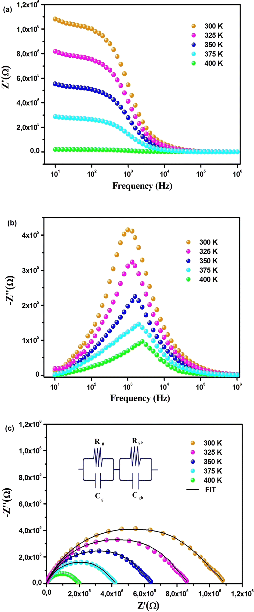 | ||
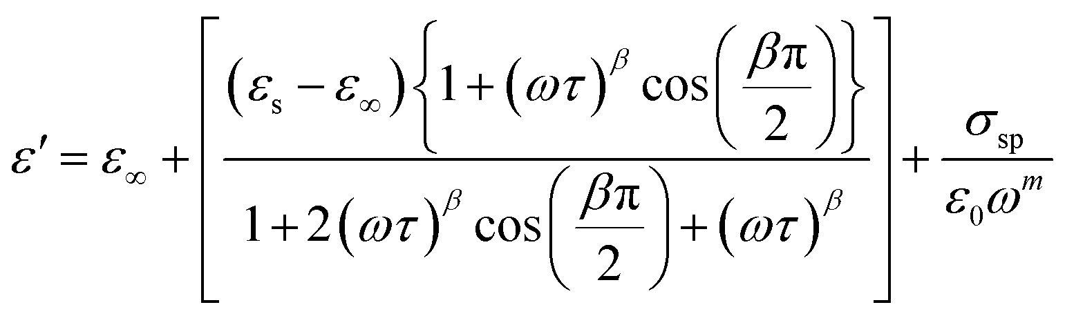
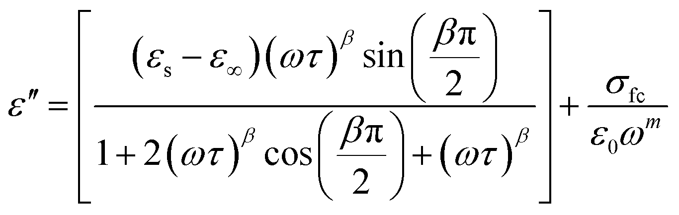
| Fig. 5 Temperature-dependent frequency analysis of (a) Z′(ω) and (b) Z′′(ω) for Cs2ZrCl6. (c) Impedance analysis of Cs2ZrCl6 using Cole–Cole plots at various temperatures (equivalent circuit displayed in inset). | ||
Fig. 5(b) depicts the variation of the loss factor (Z′′) as a function of frequency and temperature. At low temperatures, immobile species/electrons, and at high temperatures, defects/vacancies may be a valid reason behind the relaxation process. A well-defined characteristic peak, conventionally termed as the “relaxation frequency,” has been observed for each spectrum. The width of the peak indicates a significant deviation from an ideal Debye-type nature.7 The movement of long-range charge carriers is primarily responsible for transport below the peak loss frequency, and it is contributed to by the motion of localized carriers above the relaxation frequency. The shift of the relaxation peak towards a high-frequency regime with temperature indicates a thermally dependent relaxation mechanism. Furthermore, the peak height decreases with temperature, suggesting that grain/grain boundary resistance decreases with temperature.15
Fig. 5(c) illustrates the complex impedance diagrams Z′′ = f(Z′) of the compound Cs2ZrCl6. The experimental points are located on arcs passing close to the origin and centered below the real axis. This suggests that the conduction in this material does not adhere to the Debye model; instead, it follows the Cole–Cole model.29 The decreasing nature of the semi-circle radii with increasing temperature in the Cole–Cole plot again confirms the NTCR behavior of the material.7 This also indicates that the conduction process is thermally activated, and the material exhibits semiconductor characteristics. Impedance spectra at all temperatures are fitted using ZView software, and the desired circuit model is obtained in this case by connecting two parallel RC elements in series.30 Table 2 compiles the parameters of the equivalent circuit for the compound Cs2ZrCl6 derived from the best fit performed on the curves of Z′ and Z′′ as a function of angular frequency. The variation in grain boundary capacitance (Cgb), as depicted in Table 2, tends to increase with temperature. As trapped charge carriers decrease with rising temperature, the width of the barrier layer becomes relatively small at high temperatures. Consequently, the grain boundary capacitance increases with temperature.16
| Temperature (K) | Rg (kΩ) | Cg (nF) | Rgb (kΩ) | Cgb (pF) |
|---|---|---|---|---|
| 300 | 63.72 | 2.35 | 929.67 | 10.38 |
| 325 | 47.11 | 2.78 | 724.81 | 16.87 |
| 350 | 34.56 | 3.85 | 542.15 | 22.41 |
| 375 | 23.89 | 4.75 | 352.38 | 27.95 |
| 400 | 11.61 | 5.32 | 169.19 | 32.25 |
The variation of the dielectric constant with frequency was studied in the temperature range of 300 to 400 K. Fig. 6(a) and (b) show that at a particular temperature, the dielectric constant is high in the low-frequency region and gradually decreases with increasing frequency. The variation of the real part of the permittivity with frequency (Fig. 6(a)) can be explained by Maxwell–Wagner interfacial polarization, in accordance with Koop's phenomenological theory.7 In Cs2ZrCl6, molecules with permanent dipolar moments can change their orientation along the direction of the electric field in the low-frequency region. Thus, in this region, dipoles easily follow the quasi-static field, causing an increase in the dielectric constant ε′(ω).31,32 However, with increasing frequency, the dielectric constant gradually decreases as the dipoles are unable to follow the electric field. Consequently, the number of electrons decreases at the grain boundary in the high-frequency region. Therefore, the behavior of the real part of the dielectric response in the low-frequency region is governed by orientation and interfacial polarizations, confirming non-Debye behavior.31 The influence of ionic and electronic polarization is observed in the high-frequency domain, leading to a decrease in the dielectric constant ε′(ω). Among the four types of polarizations, orientation and interfacial polarization depend strongly on temperature. The upward trend of ε′(ω) with temperature, as shown in Fig. 6(a), is mainly due to the presence of thermally activated charge carriers and electric dipole moments.15 Under the influence of the electric field, temperature-dependent rotation of dipoles in Cs2ZrCl6 causes energy fluctuation, and consequently, the dielectric constant increases with temperature. The dielectric loss factor decreases with an increase in frequency (Fig. 6(b)). According to Koop's theory, imperfections or impurities in the material act as a potential barrier to the transport of charge carriers.33 Space charge polarization restricts partial conduction of charges until they are obstructed at a potential barrier or grain boundary. Therefore, due to the dominance of grain boundaries in the low-frequency region, electrons require more energy for jumps, leading to high dielectric loss.34 On the other hand, with increasing frequency, the effect of weakly resistive grain layers becomes important. Thus, very little energy is required for electron exchange between ions of the same molecules, resulting in a decrease in dielectric loss in the high-frequency domain. Orientation polarization requires more time than ionic or electronic polarization in the high-frequency region.34 Although all four types of polarizations are present in the low-frequency region, only ionic and electronic polarizations play a significant role in the high-frequency region, causing a decrease in the dielectric loss factor in the high-frequency region. To study the frequency variation of the dielectric constant and dielectric loss for different temperatures, the modified Cole–Cole model with DC conductivity, a correction term, was used among several popular theoretical models. The real (ε′) and imaginary (ε′′) parts of the dielectric constant can also be represented by eqn (4) and (5).
 | (4) |
 | (5) |
 | ||
| Fig. 6 Variations in (a) ε′(ω) and (b) ε′′(ω) across different temperatures. | ||
For clarity, the symbols used in these equations follow their standard definitions.15
The modified Cole–Cole plot method is a powerful analytical tool employed to investigate the frequency-dependent electrical behavior of materials, particularly dielectric materials.34 It is based on the Cole–Cole model, which describes the complex permittivity of materials as a function of frequency. In our study, we utilized this method to analyze the frequency variation of the dielectric constant and dielectric loss for different temperatures in Cs2ZrCl6.
The principle of the modified Cole–Cole plot lies in its ability to provide valuable insights into the electrical response of the material across a range of frequencies. This method allows us to distinguish between different types of conductivity present in the material, specifically free charge conductivity and space charge conductivity.35,36
The reliability of the modified Cole–Cole plot method stems from its ability to accurately capture the frequency-dependent behavior of dielectric materials, including variations in conductivity with temperature. By fitting experimental data to the Cole–Cole equations (eqn (4) and (5)), we can extract relevant parameters such as relaxation time and conductivity values, providing quantitative information about the material's electrical properties.
One of the key advantages of the modified Cole–Cole plot method is its ability to characterize the dielectric behavior of materials over a wide frequency range, from low to high frequencies. This comprehensive analysis enables us to understand the underlying mechanisms governing the electrical response of the material, including polarization processes and conduction mechanisms.
However, it's important to acknowledge the limitations of this method. The Cole–Cole model assumes certain simplifications and idealizations about the material's behavior, which may not fully capture all complexities, especially in heterogeneous or non-ideal systems. Additionally, the interpretation of the Cole–Cole plot requires careful consideration of the fitting parameters and may involve subjective judgments.37
In brief, the modified Cole–Cole plot method offers a valuable approach for studying the electrical properties of materials, including Cs2ZrCl6 in our study. Its principle, reliability, advantages, and limitations should be considered in the context of our research to ensure accurate interpretation of the results.34–37
The experimental data of ε′ and ε′′ are fitted with the modified Cole–Cole equation, and the calculated fitting parameters are listed in Table 3. It is evident that the value of space charge conductivity (σsp) and free charge conductivity (σfc) increases with temperature. The value of β is between 0 and 1, confirming the non-Debye character. The relaxation time decreases with increasing temperature.
| Parameter | Temperature | ||||
|---|---|---|---|---|---|
| 300 K | 325 K | 350 K | 375 K | 400 K | |
| τ (10−3) | 12.991 | 10.426 | 7.057 | 5.684 | 3.272 |
| β | 0.654 | 0.702 | 0.868 | 0.746 | 0.631 |
| m | 0.687 | 0.755 | 0.794 | 0.837 | 0.866 |
| σsp (10−3) | 0.147 | 0.338 | 0.750 | 1.142 | 1.672 |
| σfc (10−2) | 0.057 | 0.148 | 0.987 | 1.595 | 2.288 |
In sum, Cs2ZrCl6 demonstrates a notably high dielectric constant and minimal dielectric loss in comparison to other inorganic metal halide perovskites. Specifically, Cs2ZrCl6 exhibits a higher dielectric constant when juxtaposed with compounds such as Cs2TiBr6, Cs2MSbBr6 (where M = Cu, Ag), and Cs2MBiCl6 (where M = Cu, Ag).7,8,38 Conversely, it showcases a lower dielectric loss when contrasted with compounds like CsPbBr3, CsPbI3, and CsCuCl3.16,39,40
The high dielectric constant and negligible dielectric loss exhibited by Cs2ZrCl6 are crucial aspects of its electrical behavior with significant practical implications. A high dielectric constant enables efficient electrical energy storage under an applied electric field, making the material well-suited for applications such as capacitors and energy storage devices. Additionally, the minimal dielectric loss ensures minimal energy dissipation, particularly in high-frequency applications, enhancing the material's suitability for telecommunications and high-frequency circuits. These properties contribute to improved device performance, stability, and reliability. Cs2ZrCl6's dielectric characteristics hold promise for various practical applications, including enhanced energy harvesting efficiency and improved signal transmission in electronic systems. Further research can explore optimization strategies for specific applications and delve into the underlying mechanisms driving its unique dielectric behavior, paving the way for advanced technologies leveraging these promising properties.
The variation of the real part (M′) of the electric modulus with frequency at different temperatures is depicted in Fig. 7(a). At low frequencies, M′ reaches an almost zero value, indicating negligible electrode polarization effects. As the frequency increases, M′ rises and eventually reaches a constant asymptotic value (M∞) around the frequency of 105 Hz, indicating a relaxation process in Cs2ZrCl6. Fig. 7(a) illustrates that M′ decreases with an increase in temperature, suggesting short-range mobility of charge carriers within the Cs2ZrCl6 material.39 Fig. 7(b) illustrates the variation of the imaginary part (M′′) of the modulus with frequency at various temperatures. All curves exhibit an associated asymmetric peak, known as the relaxation peak, which shifts to a higher frequency with temperature, suggesting a temperature-dependent relaxation mechanism.16 The asymmetrical nature of the M′′ peaks indicates the non-Debye response of the sample. The variation of M′′ with frequency comprises two regions; the left side (below fmax) is associated with the long-distance movement of the active charge carrier within the Cs2ZrCl6 compound, and the right side (above fmax) is linked to localized displacement. Thus, the relaxation peak indicates the transition from long-distance mobilization to short-distance mobility of charge carriers in Cs2ZrCl6.15 The fit of the modified KWW function (eqn (6)) is confirmed by the solid line in Fig. 7(b), while Table 4 summarizes the values of various parameters.
 | (6) |
 | ||
| Fig. 7 Variations in (a) M′(ω) and (b) M′′(ω) across different temperatures. (c) Quantifying activation energy in Cs2ZrCl6 using Arrhenius analysis. | ||
| Temperature (K) | a | b |
|---|---|---|
| 300 | 0.487 | 0.466 |
| 325 | 0.511 | 0.496 |
| 350 | 0.548 | 0.527 |
| 375 | 0.580 | 0.543 |
| 400 | 0.613 | 0.575 |
The symbols used in this equation follow their standard definitions.16
The values of parameters a and b increase with temperature, suggesting that M′′(ω) approaches the ideal Debye-type response as the temperature rises.40 The average activation energy of charge carriers can be estimated from the Arrhenius equation (eqn (7)).
 | (7) |
The symbols used in this equation follow their standard definitions.16
The value of 0.172 eV represents the activation energy derived from the slope of the least squares fit of the ln![[thin space (1/6-em)]](https://www.rsc.org/images/entities/char_2009.gif) τ vs. 1000/T graph (Fig. 7(c)).
τ vs. 1000/T graph (Fig. 7(c)).
The variation of AC conductivity with frequency at different temperatures is illustrated in Fig. 8(a). The conductivity estimated in the low-frequency region is attributed to DC conductivity, and the conductivity in the high-frequency region is attributed to AC conductivity.41 The curves appear flattened in the low-frequency region, which is due to the contribution of DC conductivity, which is independent of frequency and temperature-dependent. However, the electrical conductivity curves exhibit a strong frequency dispersion with increasing frequency, where charge species accumulated at grain boundaries have enough energy to overcome the barrier as the temperature increases.7 Modeling of these curves (Fig. 8(a)) is carried out using the Jonscher equation (eqn (8)), showing good agreement between theoretical and experimental curves.
| σAC(ω) = σDC + σ0fs | (8) |
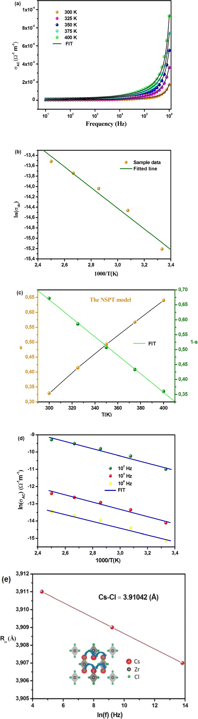 | ||
| Fig. 8 (a) Frequency and temperature dependence of AC conductivity. (b) Arrhenius plot. (c) Temperature-dependent changes in s and (1 − s). (d) Frequency-dependent analysis of ln(σac) with temperature. (e) Frequency-based analysis of the Rω parameter. | ||
The symbols used in this equation follow their standard definitions.15
The AC conductivity deduced from the Jonscher law is characterized by Arrhenius behavior (eqn (9)).42
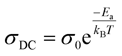 | (9) |
The symbols used in this equation follow their standard definitions.7
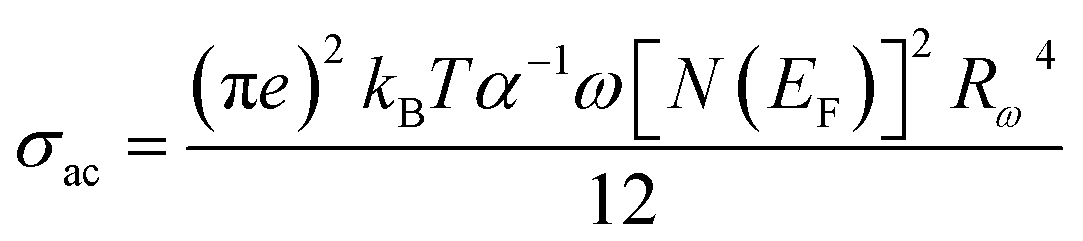
Fig. 8(b) represents the thermal variation of ln(σdc). The activation energy value for Cs2ZrCl6, which is close to the value obtained from M′′ spectra, is 0.179 eV. Fig. 8(c) presents the temperature dependence of the exponent s. According to the NSPT model, the exponent s increases with temperature, suggesting the hopping of small polarons in the Cs2ZrCl6 compound.43 In fact, in Cs2ZrCl6, negatively charged [ZrCl6]2− ions exist in the environment of Cs+ ions, but the two charge centers do not coincide, resulting in a partially polar material. The polaron forms as soon as the localized charge approaches the compound and moves towards the nearest neighboring positions.16 The polaron remains stable at this position (“successful jump”) or moves in the opposite direction after moving to a new configuration to achieve a partially relaxed configuration, also called “unsuccessful jump.” Due to the successful jump of the polaron, the non-dispersive behavior of AC conductivity emerges at low frequency.15 However, multiple jumps become unsuccessful as the frequency increases. Therefore, at high frequency, conductivity tends to become dispersive. It is believed that lattice distortion, not considered in the quantum mechanics of electron tunneling effects, triggers a polaron in most inorganic halide-based perovskite materials. Polarons can cause a high degree of local lattice distortion when formed by adding a charge carrier to a site. The lattice distortions of these small polarons do not overlap since they are confined.7 The tunneling effect of polarons or trapped carriers at structural defects could explain, at high temperatures, AC conductivity. Fig. 8(c) shows the variation of (1 − s) with temperature. The fitting of the curve was used to determine the value of Wm, which is equal to 0.111 eV (eqn (10)).
 | (10) |
The symbols used in this equation follow their standard definitions.15
Fig. 8(d) presents the variation of Cs2ZrCl6 AC conductivity with temperature. This figure clearly indicates that theoretical calculations correspond well with experimental data (eqn (11)).
 | (11) |
 | (12) |
The symbols used in this equation follow their standard definitions.7
The calculated fitting parameters are presented in Table 5. The values of the density of states N(EF) are suitable for localized states. Table 5 illustrates the variation of the parameters and N(EF) with frequency. An increase in both parameters α and N(EF) with frequency is observed, consistent with literature. The calculated Rω values from eqn (12) are presented in Table 5. The variation of the jump distance (Rω) with frequency is shown in Fig. 8(e). The values of Rω are of the same order as the Cs–Cl interatomic distance (3.907–3.911 Å) (Crystallographic Information File (CIF) with the code mp-638729). Additionally, the value of the jump distance decreases more rapidly as the frequency increases. This behavior suggests that charge carriers transition from long distance to short distance via tunneling.7 This behavior may be the reason for the increase in N(EF) (∼1022 eV−1 cm−3) with frequency.15 The Cs–Cl distance (3.910 Å) and Rω values (3.907–3.911 Å) are close, implying that AC conductivity in Cs2ZrCl6 is facilitated by the movement of small polarons due to the mobility of Cs+ in Cs2ZrCl6.
| Frequency (Hz) | α (Å−1) | N(EF) (eV−1 cm−3) | Rω (Å) |
|---|---|---|---|
| 102 | 0.69 | 2.68 × 10²² | 3.911 |
| 104 | 0.75 | 5.01 × 10²² | 3.909 |
| 106 | 0.79 | 7.34 × 10²² | 3.907 |
The NSPT conduction mechanism plays a crucial role in understanding the electrical conductivity behavior of Cs2ZrCl6 material. NSPT is a transport mechanism that involves the movement of small polarons through a lattice structure via tunneling processes.44 In the case of Cs2ZrCl6, the material comprises negatively charged [ZrCl6]2− ions surrounded by Cs+ ions, creating a partially polar environment (inset of Fig. 8(e)). The NSPT mechanism arises due to the non-coincidence of the charge centers of the constituent ions, resulting in the formation of small polarons when a localized charge approaches the compound. These small polarons exhibit stable configurations when they successfully jump to adjacent lattice sites, contributing to non-dispersive behavior in AC conductivity at low frequencies. However, as the frequency increases, multiple jumps become unsuccessful, leading to dispersive behavior in conductivity. This transition from non-dispersive to dispersive behavior is attributed to the inability of polarons to move freely within the lattice structure at higher frequencies. The significance of the NSPT conduction mechanism in Cs2ZrCl6 lies in its ability to elucidate the electrical transport properties of the material, particularly in understanding the frequency-dependent behavior of AC conductivity. By considering NSPT, we can gain insights into the underlying mechanisms governing charge transport, including the role of lattice distortion and the mobility of charge carriers. Moreover, the applicability of NSPT in Cs2ZrCl6 material is supported by experimental observations, as evidenced by the good agreement between theoretical calculations and experimental data (Fig. 8(d)). The calculated fitting parameters, such as the jump distance (Rω) and density of states (N(EF)), align with the material's crystallographic properties and provide valuable information about the mobility of charge carriers. Anyway, the electric and dielectric findings presented in this study necessitate a comprehensive non-contact mode Atomic Force Microscopy (AFM) analysis to examine the topography and surface roughness of the Cs2ZrCl6 pellet.
In summary, the NSPT conduction mechanism offers a fundamental understanding of the electrical conductivity behavior in Cs2ZrCl6 material, highlighting the role of small polarons and their interaction with the lattice structure. By elucidating the NSPT mechanism, we can further explore the material's electrical properties and its potential applications in various technological fields.
4. Conclusions
A comprehensive study was carried out on the synthesis of Cs2ZrCl6 using a regulated cooling technique, followed by an in-depth analysis of its structural, optical, and dielectric characteristics. XRD analysis has confirmed the successful formation of polycrystalline Cs2ZrCl6 without any ambiguity. Upon investigating the morphology, nanoparticles with an approximate size of 46 nanometers were observed. The perovskite being studied displays a captivating array of properties, distinguished by a significantly high dielectric constant and negligible dielectric loss when subjected to high-frequency situations. The material's unique attributes offer considerable potential for a diverse array of applications. By employing a modified Cole–Cole plot as the foundation of our analytical method, we can efficiently measure two separate types of conductivity: free charge conductivity and space charge conductivity. Remarkably, as the temperature increases, both forms of conductivity display a noticeable rise in their respective magnitudes. The examination of AC conductivity has been comprehensively conducted, with a particular emphasis on explaining the NSPT conduction mechanism. The extensive investigation conducted in this study provides a deep comprehension of the material's properties while emphasizing its potential value for diverse practical uses. Additionally, a thorough examination of dielectric properties has been performed, providing crucial information regarding the unique contributions of grain and grain boundary components to the overall impedance behavior. The electric modulus curve, when examined, exhibits an asymmetrical shape, which calls for an investigation employing the KWW relation. The discrepancy between Debye-type behavior and the imaginary part of the electric modulus becomes less pronounced with an increase in temperature, which is an important observation. Using data from modulus spectra and DC conductivity measurements, the activation energy has been calculated. The striking similarity between the relaxation behavior and the conduction mechanism within the material is evident from the closely matching activation energy values. The simplicity of its design and the ease of fabrication could make this material an attractive option for developing energy harvesting devices with multiple layers. The favorable energy bandgap obtained, along with the determined dielectric constant, evaluated relaxation time, and most importantly, the measured conductivity, all suggest that this material holds promise as a new and valuable perovskite for energy harvesting applications.Conflicts of interest
There are no conflicts to declare.Acknowledgements
The authors extend their appreciation to the Deputyship for Research & Innovation, Ministry of Education in Saudi Arabia for funding this research work through the project number ISP23-164.References
- S. Al-Qaisi, A. M. Mebed, M. Mushtaq, D. P. Rai, T. A. Alrebdi, R. A. Sheikh, H. Rached, R. Ahmed, M. Faizan, S. Bouzgarrou and M. A. Javed, J. Comput. Chem., 2023, 44, 1690–1703 CrossRef CAS PubMed.
- S. Ahmed, A. S. Hakeem, A. Alzahrani, M. Parvaz, A. Ahmed and S. Hussain, ACS Appl. Energy Mater., 2024, 7(4), 1382–1397 CrossRef CAS.
- T. Zelai, Phys. Scr., 2023, 98, 045802 CrossRef.
- K. Raj and A. P. Das, Environ. Chem. Ecotoxicol., 2023, 5, 79–85 CrossRef CAS.
- M. H. Boskabady, N. Marefati, T. Farkhondeh, F. Shakeri, A. Farshbaf and M. H. Boskabady, Environ. Int., 2018, 120, 404–420 CrossRef CAS PubMed.
- R. Kalthoum, M. B. Bechir, A. B. Rhaiem and M. H. Dhaou, Opt. Mater., 2022, 125, 112084 CrossRef CAS.
- M. B. Bechir and F. Alresheedi, RSC Adv., 2024, 14, 1634–1648 RSC.
- M. B. Bechir and M. H. Dhaou, RSC Adv., 2023, 13, 17750–17764 RSC.
- J.-N. Lv, J. Zhang, Y. Liu, S. Zhang, X. Deng, M. Xu, X. Lei, Z. Chen and C.-Y. Yue, Dalton Trans., 2024, 53, 4698–4704 RSC.
- Y. Ru, J. Zhou, J. Ju, H. Song, Z. Liu, L. Zhang, X. Liu, G. Zhong, Y. Xue, I. R. Panneerselvam, L. Manna and S. Lu, J. Am. Chem. Soc., 2024, 146(11), 7658–7667 CrossRef PubMed.
- Y. Tang, M. Deng, Z. Zhou, C. Kang, Y. Wang and Q. Liu, Coord. Chem. Rev., 2024, 499, 215490 CrossRef CAS.
- A. Ajayakumar, C. Muthu, M. G. Basavarajappa, A. V. Dev, R. Nishikubo, S. Chakraborty, A. Saeki, L. Dou and C. Vijayakumar, Adv. Funct. Mater., 2024, 34, 2304899 CrossRef CAS.
- X. Yun, J. Nie, H. Hu, H. Zhong, D. Xu, Y. Shi and H. Li, J. Lumin., 2024, 268, 120379 CrossRef CAS.
- C. A. Hutchison and B. W. Mangum, J. Chem. Phys., 1960, 32, 1261–1262 CrossRef.
- M. B. Bechir and M. H. Dhaou, RSC Adv., 2021, 11, 21767–21780 RSC.
- M. B. Bechir and M. H. Dhaou, Mater. Res. Bull., 2021, 144, 111473 CrossRef CAS.
- A. Abfalterer, J. Shamsi, D. Kubicki, C. N. Savory, J. Xiao, G. Divitini, W. Li, S. Macpherson, K. Gałkowski, J. L. MacManus-Driscoll, D. O. Scanlon and S. D. Stranks, ACS Mater. Lett., 2020, 2, 1644–1652 CrossRef CAS PubMed.
- S. Berri and N. Bouarissa, Phys. Status Solidi B, 2023 DOI:10.1002/pssb.202300280.
- T. Zhao and G. Chen, Opt. Mater., 2023, 136, 113355 CrossRef CAS.
- L. Yin, H. Wu, W. Pan, B. Ye, P. Li, J. Luo, G. Niu and J. Tang, Adv. Opt. Mater., 2019, 7, 1900491 CrossRef CAS.
- S. Bhaumik, S. Ray and S. K. Batabyal, Mater. Today Chem., 2020, 18, 100363 CrossRef CAS.
- F. Zhang, Y. Zhou, Z. Chen, M. Wang, Z. Ma, X. Chen, M. Jia, D. Wu, J. Xiao, X. Li, Y. Zhang, Z. Shi and C. Shan, Adv. Mater., 2022, 34, 2204801 CrossRef CAS PubMed.
- M. B. Bechir, A. Almeshal and M. H. Dhaou, Mater. Res. Bull., 2023, 157, 112012 CrossRef CAS.
- M. B. Bechir, M. H. Dhaou and S. M. Altrifi, Mater. Res. Bull., 2023, 167, 112381 CrossRef.
- M. B. Bechir and S. Znaidia, Phys. Chem. Chem. Phys., 2023, 25, 19684–19692 RSC.
- M. B. Bechir and F. Alresheedi, Opt. Mater., 2024, 147, 114621 CrossRef.
- R. Kalthoum, M. B. Bechir and A. B. Rhaiem, Phys. E, 2020, 124, 114235 CrossRef CAS.
- I. Romdhane, M. B. Bechir and M. H. Dhaou, Phys. E, 2022, 136, 115008 CrossRef CAS.
- M. B. Bechir, A. Almeshal and M. H. Dhaou, Ionics, 2022, 28, 5361–5376 CrossRef CAS.
- M. B. Bechir, K. Karoui, M. Tabellout, K. Guidara and A. B. Rhaiem, Phase Transitions, 2015, 91, 901–917 CrossRef.
- A. García-Fernández, J. M. Bermúdez-García, S. Castro-García, A. L. Llamas-Saiz, R. Artiaga, J. López-Beceiro, S. Hu, W. Ren, A. Stroppa, M. Andújar and M. A. Señarís-Rodríguez, Inorg. Chem., 2017, 56, 4918–4927 CrossRef PubMed.
- P. Thongbai, S. Tangwancharoen, T. Yamwong and S. Maensiri, J. Phys.: Condens. Matter, 2008, 20, 395227 CrossRef.
- C. G. Koops, Phys. Rev., 1951, 83, 121 CrossRef CAS.
- P. Sengupta, P. Sadhukhan, A. Ray, R. Ray, S. R. Bhattacharyya and S. Das, J. Appl. Phys., 2020, 127(20), 204103 CrossRef CAS.
- P. Thongbai, S. Tangwancharoen, T. Yamwong and S. Maensiri, J. Phys.: Condens. Matter, 2008, 20, 395227 CrossRef.
- S. Patra, P. Sengupta, A. Ray, A. Roy and S. Das, Ceram. Int., 2018, 44, 14236 CrossRef CAS.
- D. K. Rana, S. K. Singh, S. K. Kundu, S. Roy, S. Angappane and S. Basu, New J. Chem., 2019, 43, 3128 RSC.
- S. Znaidia and M. B. Bechir, Ionics, 2024, 30, 1177 CrossRef CAS.
- P. Maji, S. Chatterjee and S. Das, Ceram. Int., 2019, 45, 6012–6020 CrossRef CAS.
- P. Maji, A. Ray, P. Sadhukhan, S. Chatterjee and S. Das, J. Appl. Phys., 2018, 124(12), 124102 CrossRef.
- S. Pujaru, P. Maji, P. Sadhukhan, A. Ray, B. Ghosh and S. Das, J. Mater. Sci.: Mater. Electron., 2020, 31, 8670–8679 CrossRef CAS.
- M. B. Bechir and A. B. Rhaiem, Phys. E, 2021, 130, 114686 CrossRef.
- M. B. Bechir, K. Karoui, M. Tabellout, K. Guidara and A. B. Rhaiem, J. Appl. Phys., 2014, 115, 203712 CrossRef.
- S. R. Elliott, Adv. Phys., 1987, 36, 135–217 CrossRef CAS.
Footnote |
| † Electronic supplementary information (ESI) available. See DOI: https://doi.org/10.1039/d4ra02031f |
| This journal is © The Royal Society of Chemistry 2024 |