
 Open Access Article
 This Open Access Article is licensed under a Creative Commons Attribution-Non Commercial 3.0 Unported Licence
High-performance self-powered ultraviolet photodetector based on a ZnO/CuPc inorganic/organic heterojunction
Lingling Chu ,
Chao Xu*,
Zhengping Li and
Chao Nie
,
Chao Xu*,
Zhengping Li and
Chao Nie
School of Integrated Circuits, Anhui University, Hefei 230601, China. E-mail: graymagpie@163.com
First published on 30th April 2024
Abstract
A self-powered photodetector (PD) based on n-type ZnO/p-type small-molecule copper(II) phthalocyanine (CuPc) inorganic/organic heterojunction film deposited on FTO substrate was constructed by simple solution spin-coating and thermal evaporation technology. The designed heterojunction device exhibits typical photoresponse behavior under zero bias, indicating that the device possesses a self-powered characteristic. This may benefit from the formation of a built-in electric field in the heterojunction, which can effectively separate electron–hole pairs. Specifically, the optimal performances of the device appear at a wavelength of 365 nm and light intensity of 0.03 mW cm−2, achieving on/off ratio of ∼245.88 (29.88), responsivity (Rp) of ∼227.11 mA W−1 (0.39 mA W−1), detectivity (D*) of ∼7.63 × 10¹¹ Jones (∼7.53 × 10⁹ Jones) and EQE of ∼77.23% (0.14%) at +2 V (0 V) bias voltage. In addition, the device has potential application in weak light detection. Therefore, the construction of inorganic/organic heterojunctions may provide a feasible strategy for the development of high-performance, self-powered and wavelength-selective PDs.
1. Introduction
Recently, heterojunctions formed by semiconductor materials of different types have been widely applied in common photovoltaic devices, such as PDs,1 solar cells2 and other photoelectric conversion devices.3 This is mainly due to the formation of an internal electric field at the heterojunction interface that can regulate internal charge carriers, effectively separate electron–hole pairs and facilitate the transport of the carriers in devices based on such heterojunctions.4 Unfortunately, pure organic or inorganic semiconductors have some inherent defects that degrade optoelectronic performance or limit application range. Therefore, effective solutions, such as the construction of heterojunctions consisting of organic/inorganic semiconductors, demonstrating advantages in improving carrier migration and reducing recombination rate, have been proposed. Furthermore, this is beneficial for the development and application of high-performance optoelectronic devices. Especially, high-performance optoelectronic devices constructed with heterojunction structures composed of p-type organic semiconductors and n-type inorganic semiconductor materials have received widespread attention from researchers.Among numerous inorganic semiconductor materials, ZnO is widely used in various microelectronic devices such as optoelectronic conversion and piezoelectric devices. For example, ZnO has been applied in UV detection devices due to some important characteristics, such as wide bandgap (∼3.32 eV), high exciton binding energy (∼60 meV) and high photoconductivity.5,6 To be more convenient for serving people's daily lives concerning ZnO-based optoelectronic devices, higher requirements for high-performance ZnO-based optoelectronic devices have been proposed, such as high on/off ratio, Rp and D*. Therefore, to promote the application of n-type semiconductor materials in optoelectronic devices, implementing effective solutions to further study and optimize the performance is necessary. Previously reported have been transition metal element doping (Cu, Co, Mn, Ni and Fe),6 coating UV-sensitive polymers to modify the surface of nanostructures (such as polyacrylonitrile and polystyrene sulfate),7 constructing device structures with p–n heterojunctions (common p-type materials such as poly(9,9-dihexylfluorene); Spiro MeOTAD; polyaniline (PANI) and copper thiocyanide (CuSCN)) and post-treatment for devices.8 In addition, accelerating the charge transfer to the electrode and avoiding carrier recombination are nonnegligible problems that need to be considered in the design of optoelectronic device structures. Therefore, to build a p–n junction to adjust carrier transport is particularly important.9,10 Materials like phthalocyanines (Pcs) were proven to have low molecular weight and flat organic molecular characteristics, showing great potential in the application of optoelectronic devices.11 A typical p-type organic semiconductor material, copper phthalocyanine (CuPc), has excellent π–π stacking characteristics and photoresponse, which is often used as the hole transport layer of optoelectronic devices,12,13 such as solar cells,14 field effect transistors15,16 and light-emitting diodes.17 In addition, a CuPc film fabricated by thermal evaporation technology exhibits positive stacking characteristics, high hole mobility, excellent chemical stability, thermal stability and hydrophobicity.18,19 This also implies that a device may be able to maintain long-term performance stability in humid environments, further prolonging the service life of the device.
In this work, a vertical heterojunction was constructed with p-type semiconductor CuPc to optimize the performance of an n-type semiconductor ZnO-based PD. It is believed that the presence of the CuPc/ZnO vertical heterojunction can facilitate charge transfer, where the CuPc film was deposited on the surface of ZnO through thermal evaporation technology. Additionally, the PD based on CuPc/ZnO vertical heterostructure exhibits a typical self-powered characteristic and achieves excellent optoelectronic performances. Specifically, low dark current (7.84 × 10⁻¹⁰ A) and high photocurrent (6.09 × 10⁻⁶ A), Rp (227.11 mA W−1), D* (7.63 × 10¹¹ Jones) and EQE (77.23%) can be obtained. This result implies the possible potential of organic/inorganic semiconductor hybrid structures in the field of optoelectronic devices.
2. Experimental details
2.1 Preparation of ZnO film
First, FTO glass is pretreated by ultrasonic cleaning with acetone, alcohol and distilled water for 10 min each. Then, residual water on the surface is blown away with nitrogen gas. Finally, the as-cleaned FTO glass is treated using plasma equipment for 15 min to improve the hydrophilicity and surface adhesion for film formation. The preparation method of ZnO has been proposed in previous reports.20 In brief, this involves dissolving zinc acetate in ethanol (40 mM) and continuously stirring until the solution becomes transparent, then coating the as-prepared solution on the as-treated FTO conductive glass using spin coating technology (2000 rpm; 1 min). Additionally, annealing treatment is necessary (150 °C; 10 min). Finally, samples were annealed in a muffle furnace to obtain a high-quality ZnO film (250 °C; 1 h).2.2 Preparation and characterization of device
The preparation method of the CuPc film has been proposed in previous reports. Purchased CuPc powder (sublimed grade, dye content 99%) is placed in a high-temperature-resistant tungsten boat, and the CuPc film is deposited on the as-prepared ZnO film via thermal evaporation. The basic pressure in the evaporation chamber is less than 4 × 10⁻⁴ Pa, the control current is ≈75–80 A, the deposition rate is ≈0.2–0.4 Å s−1, and the deposition time is ≈15 min. The final visible blue film is covered on the surface of the ZnO film. For electrode production, a silver slurry with a diameter of ∼1–2 mm is dropped onto the CuPc film as the top electrode, and the FTO conductive glass is used as the bottom electrode. The photosensitive area of the device is ∼0.09 cm2. Subsequently, the complete device was placed in a vacuum oven to dry the silver paste electrode (60 °C; 3 h). Morphological characterization of the CuPc film coated on the ZnO film was conducted using SEM technology (TESCAN MIRALMS). The absorption of the material was tested using a UV visible near-infrared spectrophotometer (U-4100). The photoelectric testing equipment of the device consists of a light source (xenon arc lamp (Newport) and a monochromator) and a source meter (Keysight B2901A precision source/measurement unit).3. Results and discussion
The PD based on the ZnO/CuPc vertical heterojunction is mainly manufactured through spin coating and thermal evaporation and served as the photosensitive layer of the device. The Ag slurry is deposited on the CuPc film, and the bottom conductive glass substrate provides a conductive channel, which can collect the injected photogenerated carriers. The complete device structure is shown in Fig. 1(a). Additionally, Fig. 1(b) shows the generation and transfer process of the carriers in the entire device under light radiation. It can be seen that due to the absorption of high-energy photons, electrons in the valence band of ZnO and CuPc are excited to reach the conduction band as photogenerated carriers, enriching the types of carriers and further increasing the carrier concentration of the device.21,22 Therefore, the performances of devices based on ZnO are significantly improved by utilizing the introduction of CuPc. Importantly, once reaching thermal equilibrium condition, an interface depletion region will be formed in the heterojunction structure composed of p-type CuPc and n-type ZnO, and the built-in electric field formed will bend the energy band at the interface, ultimately providing motivation for carrier transport. Driven by the electric field, electrons located in the conduction band of CuPc can flow to ZnO, while holes in the valence band of ZnO can move towards CuPc, reducing the recombination rate of electron–hole pairs and accelerating the collection of carriers at the electrode.23,24 On the contrary, without external light radiation, the built-in electric field at the interface will prevent the transfer of carriers to electrodes, leading to the generation of low dark current. The typical self-powered photoresponse characteristics of the CuPc/ZnO heterojunction PD (PDZP) are shown in Fig. 1(c and d). Based on test results, the measured dark current of the device is about 2.48 × 10⁻⁸ A (7.84 × 10⁻¹⁰ A) at +2 V (0 V). However, once the device is exposed to light with a wavelength of 365 nm and intensity of 7.57 mW cm−2, the photocurrent of PDZP increases sharply, reaching about 6.09 × 10⁻⁶ A (2.34 × 10⁻⁸ A) at +2 V (0 V). The same phenomenon is found in the time-dependent photoresponse cycle test results (Fig. 1(d)).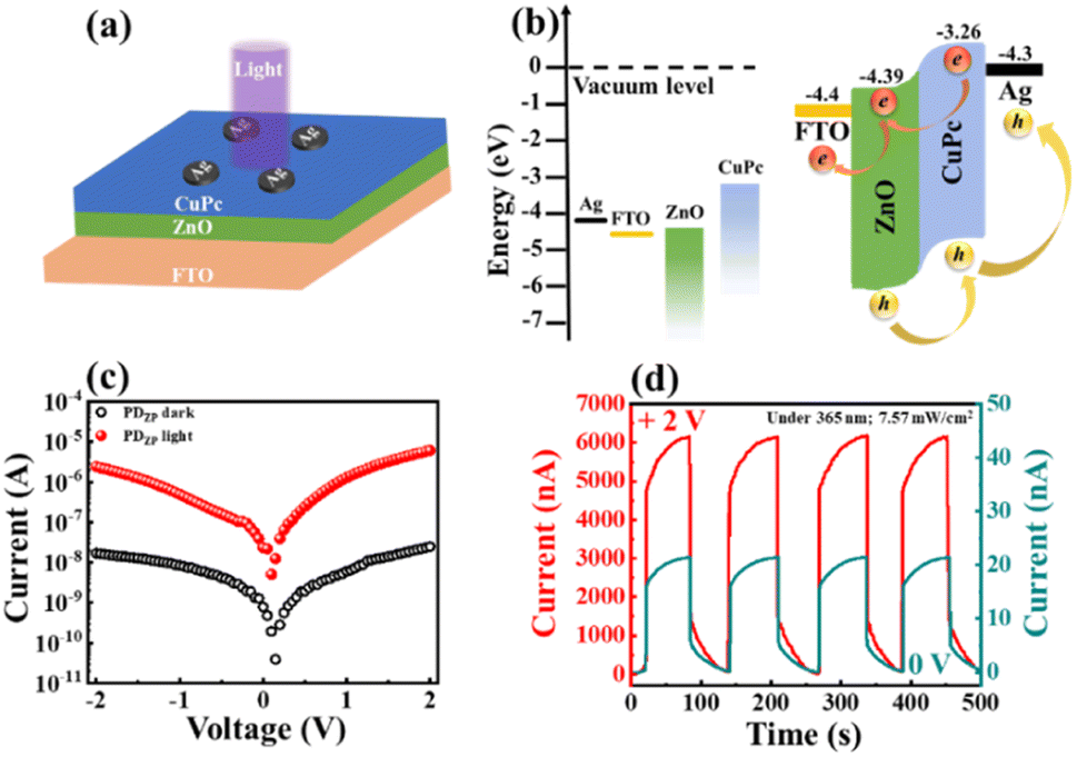 | ||
| Fig. 1 (a) Schematic diagram of the photodetector based on the CuPc/ZnO organic/inorganic hybrid vertical heterojunction. (b) Energy level distribution of CuPc/ZnO. (c) Comparison of dark and light current of the device. (d) Time-dependent current curves of the device at 0 V and +2 V. | ||
In addition, the morphology and optical properties of the photosensitive layer were investigated, as shown in Fig. 2. To fully demonstrate the morphology of the ZnO/CuPc film, the top and cross-sectional morphology of the sample were characterized using SEM technology, as shown in Fig. 2(a and b). According to the top view (Fig. 2(b)), it can be observed that dense and uniform CuPc nanoparticles are tightly connected to form a CuPc film, which may be beneficial for carrier transport. Specifically, the size of the CuPc nanoparticles was measured to be approximately 31.25 nm. The cross-sectional SEM image of the ZnO/CuPc layer is shown in Fig. 2(a). According to this image, the sectional morphology of ZnO and CuPc films can be clearly seen, and the thicknesses of ZnO and CuPc films were measured to be approximately 661.93 nm and 159.24 nm, respectively. Fig. 2 (b-1-b-5) describes single element mapping of C, N, Cu, O and Zn atoms in the as-prepared ZnO/CuPc film. Here, C, N and Cu come from CuPc, while O and Zn come from ZnO. This implies that the CuPc/ZnO hybrid photosensitive layer had been successfully prepared. Additionally, the surface roughness of ZnO/CuPc has an important impact on the performance of photodetectors based on the ZnO/CuPc heterojunction structure. According to a previous report,25 Tran et al. demonstrated that the reduction the ZnO surface roughness and ZnO nanoparticle size not only promotes the transport of the photogenerated carriers but also increases the charge lifetime of ZnO. The fact that the particle size of CuPc is almost uniform was also confirmed by the AFM result, as shown in Fig. 2(c). According to the test results of ZnO/CuPc film, the surface roughness of the film can also be determined to be approximately 3.84 nm. From a previous experiment, we can obtain a surface roughness of approximately 3.02 nm for the ZnO film. The AFM results revealed that the surface roughness of ZnO increased from 3.02 nm to 3.84 nm with the incorporation of CuPc. Moderately increasing surface roughness can enhance surface light scattering and the ability of the photosensitive layer to capture incident photons, which can increase luminous flux and improve the production efficiency of photogenerated electron hole pairs. Fig. 2(d) shows the UV visible absorption of the ZnO film deposited on FTO substrates, the CuPc film and the CuPc/ZnO heterojunction film. For ZnO, the maximum absorbance can be obtained at a wavelength of ∼344 nm. Moreover, the absorption spectrum of the CuPc film (Fig. 2(d)) shows two obvious absorption edges located at ∼622 nm and 694 nm, which are called Q-bands, originating from the electron conversion of π–π26,27 However, the hybrid film formed by the combination of ZnO and introduced CuPc not only improves the absorption but also broadens the range of absorption spectra. This suggests that the hybrid film may be applicable in the manufacturing of broadband optoelectronic devices. The photoluminescence (PL) test results of the three films are shown in Fig. 2(e). Compared with the original ZnO film, the intensity of ZnO/CuPc laminated film reduces significantly, indicating that the introduction of CuPc can effectively suppress the recombination of photocarriers in ZnO film.
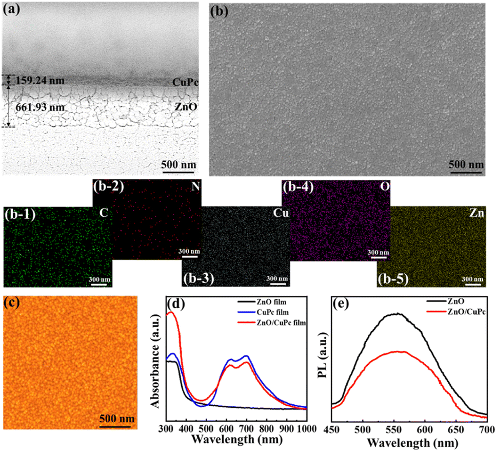 | ||
| Fig. 2 (a) Cross-section and (b) top view SEM images of the ZnO/CuPc film. (b-1, b-2, b-3, b-4 and b-5) The corresponding elemental phase maps of the ZnO/CuPc film. (c) AFM image of the ZnO/CuPc laminated film. (d) Absorbance of ZnO, CuPc and ZnO/CuPc films. (e) PL spectra of ZnO and ZnO/CuPc films. | ||
Based on the above discussion, the research work achieved the goal of improving the performance of a ZnO-based PD by utilizing the p–n junction structure established by introducing CuPc organic small molecules. Subsequently, the voltage-dependent photocurrent of the device was determined using optoelectronic testing equipment, as shown in Fig. 3(a). An increased light intensity can increase the photocurrent of the device, which may be due to the increase of carrier concentration caused by an increase of the number of photogenerated carriers. A similar trend is also reflected in Fig. 3(b and c). According to test results provided in Fig. 3(b and c), it can be observed that power-dependent on/off ratio and photocurrent of the device exhibit homologous trends at +2 V and 0 V. Specifically, taking the device photocurrent under +2 V excitation as an example, under 365 nm UV light, this is ∼638.02 nA at 0.03 mW cm−2, ∼725.13 nA at 0.08 mW cm−2, ∼978.15 nA at 0.24 mW cm−2, ∼1310.03 nA at 0.41 mW cm−2, ∼1910.30 nA at 0.78 mW cm−2, ∼3250.12 nA at 2.08 mW cm−2, ∼4410.25 nA at 3.69 mW cm−2, ∼5250.22 nA at 5.11 mW cm−2, ∼5640.53 nA at 6.39 mW cm−2 and ∼6097.80 nA at 7.57 mW cm−2. In addition, Fig. 3(d) shows the time-dependent current curves of PDZP with on/off characteristics under 365 nm radiation at 0 V bias, indicating that the device has typical self-powered characteristics. When the light is turned on, the current of the device increases sharply. Once the light is turned off, the current of the device gradually decays and returns to the original state, indicating that the device has photosensitivity to light. Furthermore, repeating the operation can reproduce the photocurrent of PDZP, indicating that the device possesses stable photoresponse characteristics. Rapid photoresponse is one of the important features in designing high-performance optoelectronic devices. Therefore, rise and decay times in single-cycle curves were recorded, calculated to be ∼3.26 s and 6.32 s, respectively. Here, the rise time is defined as the time required to rise from 20% of the maximum photocurrent to 80%, while the decay time is defined as the time required to decay from 80% of the maximum photocurrent to 20%.
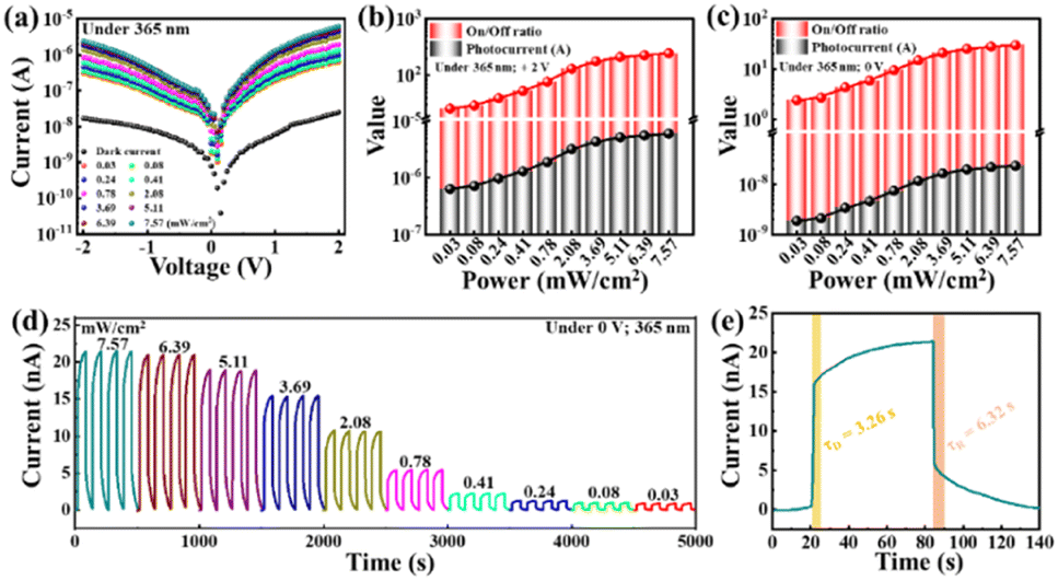 | ||
| Fig. 3 (a) Dark current and photocurrent of PDZP under 365 nm irradiation with external voltage between ±2 V. Summary of on/off ratio and photocurrent at (b) +2 V and (c) 0 V. (d) Time-dependent photocurrent of PDZP under 365 nm at 0 V. (e) Rise/decay time. | ||
Fig. 4 shows a summary of the performances of PDZP under +2 V and 0 V excitation and 365 nm UV radiation (light intensity variation between 0.03 and 7.57 mW cm−2), namely photocurrent, Rp, D*, EQE and LDR. Fig. 4(a and b) further utilizes the formula Ilight = APθ to explain the correlation between the photocurrent and light intensity, regardless of whether the bias voltage is provided, where P represents the excitation intensity of the external light source, A is a constant at a specific wavelength, and θ is also a constant. By fitting, nonlinear relationships of Ilight = AP0.44 and Ilight = AP0.52 can be obtained under +2 V and 0 V excitation, indicating that an increase of photon flux can amplify the photocurrent of the device. In addition, within the same light intensity variation range, Rp, D* and EQE of the device exhibit similar enhancement orders. At a wavelength of 365 nm and light intensity of 7.57 mW cm−2, Rp of ∼227.11 mA W−1 (0.39 mA W−1), D* of ∼7.63 × 10¹¹ Jones (7.53 × 10⁹ Jones) and EQE of ∼77.23% (0.14%) at +2 V (0 V) bias voltage were achieved. Furthermore, LDR test results of the device are shown in Fig. 4(f). The LDR of PDZP increases with the enhancement of light intensity. By fitting, nonlinear relationships of LDR = bP0.11 (for +2 V) and LDR = bP0.24 (for 0 V), where b is a constant, can be obtained. Specifically, under a wavelength of 365 nm and light intensity of 7.57 mW cm−2, the LDR of PDZP is ∼47.81 dB at +2 V and 29.51 dB at 0 V.
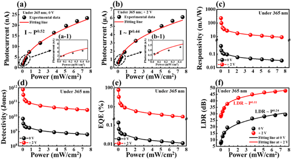 | ||
| Fig. 4 Summary of typical performance indicators of PDZP between 0.03 and 7.57 mW cm−2 at 0 V and + 2 V: (a and b) photocurrent. (a-1, -b-1) Enlarged view of photocurrent of the device between 0.03 and 0.41 mW cm−2. (c) Rp, (d) D* and (e) EQE. (f) Variation of LDR towards different light intensities. | ||
The test results of wavelength-dependent photocurrent generated by PDZP under different bias excitation at a light intensity of 7.57 mW cm−2 are shown in Fig. 5(a). Based on the data provided in Fig. 5(a), it can be observed that the device exhibits different photoresponse to different wavelengths. Similarly, Fig. 5(d) intuitively demonstrates the wavelength selectivity of the designed device. For example, under an excitation of +2 V bias, the device generates a photocurrent of ∼6097.80 nA at 365 nm, ∼3580.01 nA at 405 nm, ∼63.81.10 nA at 530 nm, ∼1870.05 nA at 625 nm, ∼895.12 nA at 730 nm, ∼36.21 nA at 880 nm and ∼25.82 nA at 970 nm. Therefore, the enhancement order of the photocurrent under +2 V bias excitation can be described as: 365 nm > 405 nm > 625 nm > 730 nm > 530 nm > 880 nm > 970 nm. A similar enhancement order is exhibited at 0 V. In addition, regardless of the presence or absence of bias excitation, the on/off ratio and photocurrent histograms at different wavelengths are shown in Fig. 5(b and c), also exhibiting the same trend. The results indicate that the optimal photocurrent and on/off ratio occur at a wavelength of 365 nm. However, once an external bias is applied to the device, the photocurrent and on/off ratio are further amplified, which may be due to the external electric field improving the transport of the charge carriers and effectively avoiding the recombination of the electron–hole pairs. For example, under the same intensity and wavelength, a photocurrent and on/off ratio of ∼6097.80 nA (23.43 nA) and 245.88 (29.88) at +2 V (0 V) can be obtained for PDZP. Compared to 0 V, these values have correspondingly increased by ∼260.26 and 8.23 times. In addition, performance indicators related to an optoelectronic device, Rp, D* and EQE, are shown in Fig. 6. According to test data provided in Fig. 6(a–c), at 0 V, the maximum Rp, D* and EQE of PDZP under a light intensity of 7.57 mW cm−2 appear at a wavelength of 365 nm, reaching ∼0.03 mA W−1, 6.28 × 10⁸ Jones and 0.01%, respectively. However, once a bias voltage is applied to the device, under same conditions, corresponding values increase by ∼297.00, 47.61 and 303.00 times, respectively, which are estimated to be ∼8.91 mA W−1, 2.99 × 10¹⁰ Jones and 3.03%.
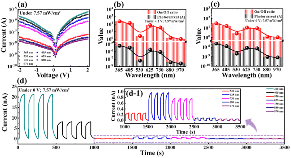 | ||
| Fig. 5 Wavelength-dependent photoresponse of PDZP under light intensity of 7.57 mW cm−2. (a) Current–voltage curves of PDZP between ±2 V. Summary of on/off ratio and photocurrent at (b) +2 V and (c) 0 V. (d) Current–time curves of PDZP at 0 V. (d-1) Enlarged view of current–time curves at 530, 625, 730 and 880 nm. | ||
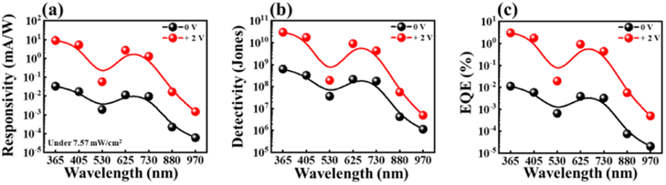 | ||
| Fig. 6 Summary of common photoelectric performances of PDZP. (a) Rp, (b) D* and (c) EQE. | ||
Table 1 compares the performance parameters of various self-powered PDs with different ZnO heterojunctions. The results indicate that under zero bias, the ZnO/CuPc inorganic/organic heterojunction may be able to achieve high-performance photodetector construction. In addition, compared with other heterojunction devices, the heterojunction device exhibits weak light detection ability.
4. Conclusion
In summary, the construction of a p–n junction by introducing organic small molecule CuPc achieved an enhancement of the photoelectric performance of a ZnO-based PD. This is mainly due to the formation of a built-in electric field at the heterojunction interface that can regulate the internal carriers, effectively separate the electron–hole pairs and accelerate carrier transport to the electrode. In addition, the deposition of the CuPc film on the surface of ZnO can modify surface defects. Based on the above discussion, the ZnO/CuPc vertical heterojunction-based PD not only possesses a self-powered characteristic but also exhibits excellent optoelectronic performance. Under light radiation with a wavelength of 365 nm and light intensity of 0.03 mW cm−2, the device achieved an on/off ratio of ∼245.88 (29.88), Rp of ∼227.11 mA W−1 (0.39 mA W−1), D* of ∼7.63 × 10¹¹ Jones (7.53 × 10⁹ Jones) and EQE of ∼77.23% (0.14%) at +2 V (0 V) bias voltage. This difference may be due to the external bias voltage being able to increase the transport rate of the carriers to the electrodes and effectively avoiding carrier recombination. Therefore, the design of the organic/inorganic heterojunction structure may be applied in the optimization of the photodetection ability of optoelectronic devices.Author contributions
Methodology, writing – original draft preparation, L. C.; software, writing – review and editing, C. X.; validation, Z. L.; resources, C. N. All authors have read and agreed to the published version of the manuscript.Conflicts of interest
There are no conflicts to declare.Acknowledgements
The authors are grateful to Anhui University for providing necessary instrumental facilities to carry out the research work.Notes and references
- T. Q. Trung, V. Q. Dang, H.-B. Lee, D.-I. Kim, S. Moon, N.-E. Lee and H. Lee, An Omnidirectionally Stretchable Photodetector Based on Organic-Inorganic Heterojunctions, ACS Appl. Mater. Interfaces, 2017, 9, 35958–35967 CrossRef CAS PubMed.
- A. Martí, Limiting Efficiency of Heterojunction Solar Cells, IEEE J. Photovoltaics, 2019, 9, 1590–1595 Search PubMed.
- İ. Candan, M. Parlak and Ç. Erçelebi, PbS quantum dot enhanced p-CIGS/n-Si heterojunction diode, J. Mater. Sci.: Mater. Electron., 2019, 30, 2127–2135 CrossRef.
- Z. Yang, L. Zhao, S. Zhang and X. Zhao, Ferroelectric-enhanced BiVO4-BiFeO3 photoelectrocatalysis for efficient, stable and large-current-density oxygen evolution, Appl. Mater. Today, 2022, 26, 101374–101384 CrossRef.
- C. Sa, X. X., X. Wu, J. Chen, C. Zuo and X. Fang, A wearable helical organic-inorganic photodetector with thermoelectric generators as the power source, J. Mater. Chem. C, 2019, 7, 13097–13103 RSC.
- F. Teng, L. Zheng, K. Hu, H. Chen, Y. Li, Z. Zhang and X. Fang, Surface oxide thin layer of copper nanowires enhanced UV selective response of ZnO film photodetector, J. Mater. Chem. C, 2016, 4, 8416–8421 RSC.
- J. Saghaei, A. Fallahzadeh and T. Saghaei, Vapor treatment as a new method for photocurrent enhancement of UV photodetectors based on ZnO nanorods, Sens. Actuators, A, 2016, 247, 150–155 CrossRef CAS.
- J. Li, S. Yin, M. M. Shirolkar, M. Li, M. Wang, X. Dong, X. Song and H. Wang, Tuning the properties of a self-powered UV photodetector based on ZnO and poly(3,4-ethylenedioxythiophene): Poly(styrenesulfonate) by hydrogen annealing of ZnO nanorod arrays, Thin Solid Films, 2017, 628, 101–106 CrossRef CAS.
- X. Zhan, D. Du and Y. Zheng, et al., Boosted photocatalytic hydrogen production over two-dimensional/two dimensional Ta3N5/ReS2 van der Waals heterojunctions, J. Colloid Interface Sci., 2023, 629, 455–466 CrossRef CAS PubMed.
- X. Zhan, H. Hou and D. Du, et al., Heterojunction engineering between 2D MoSe2 nanosheets and 1D Ta3N5 nanofibers for boosted photocatalytic hydrogen production, Mater. Today Energy, 2023, 34, 101311–101322 CrossRef CAS.
- S. Riad, Dark and photoelectric conversion properties of p-MgPc/n-Si (Organic/Inorganic) heterojunction cells, Thin Solid Films, 2000, 370, 253–257 CrossRef CAS.
- L. Zhang, Y. Yang, H. Huang, L. Lyu, H. Zhang, N. Cao, H. Xie, X. Gao, D. Niu and Y. Gao, Thickness-Dependent Air-Exposure-Induced Phase Transition of CuPc Ultrathin Films to Well-Ordered One-Dimensional Nanocrystals on Layered Substrates, J. Phys. Chem. C, 2015, 119, 4217–4223 CrossRef CAS.
- T. Fukuma, K. Kobayashi, H. Yamadaa and K. Matsushige, Noncontact atomic force microscopy study of copper-phthalocyanines: Submolecular-scale contrasts in topography and energy dissipation, J. Appl. Phys., 2004, 95, 4742–4746 CrossRef CAS.
- Q. Yuan, K. B. Lohmann, R. D. J. Oliver, A. J. Ramadan, S. Yan, J. M. Ball, M. G. Christoforo, N. K. Noel, H. J. Snaith and L. M. Herz, et al., Thermally Stable Perovskite Solar Cells by All-Vacuum Deposition, ACS Appl. Mater. Interfaces, 2022, 15, 772–781 CrossRef PubMed.
- M. M. Tavakoli, P. Yadav, D. Prochowicz and R. Tavakoli, Efficient, Hysteresis-Free, and Flexible Inverted Perovskite Solar Cells Using All-Vacuum Processing, Sol. RRL, 2020, 5, 2000552–2000559 CrossRef.
- R. R. Cranston, M. C. Vebber, J. F. Berbigier, N. A. Rice, C. Tonnelé, Z. J. Comeau, N. T. Boileau, J. L. Brusso, A. J. Shuhendler and F. Castet, et al., Thin-Film Engineering of Solution-Processable n-Type Silicon Phthalocyanines for Organic Thin-Film Transistors, ACS Appl. Mater. Interfaces, 2020, 13, 1008–1020 CrossRef PubMed.
- G. Hu, H. Zhu, Q. Dai, C. Jiang, Y. Peng, W. Lv, S. Xu, L. Sun, L. Jiang and G. F. Schneider, Operation voltage and illumination intensity dependent space-charge limited current conductions in vertical organic phototransistors based on CuPc/C60 heterojunction and graphene, Appl. Phys. Lett., 2022, 121, 123501–123508 CrossRef CAS.
- J. Xu, Y. Wang, Q. Chen, Y. Lin, H. Shan, V. A. L. Roy and Z. Xu, Enhanced lifetime of organic light-emitting diodes using soluble tetraalkyl-substituted copper phthalocyanines as anode buffer layers, J. Mater. Chem. C, 2016, 4, 7377–7382 RSC.
- C. Stecker, Z. Liu, H. Jeremy, S. Zhang, L. K. Ono, G. Wang and Q. Yabing, Atomic Scale Investigation of the CuPc-MAPbX3 Interface and the Effect of NonStoichiometric Perovskite Films on Interfacial Structures, ACS Nano, 2021, 15, 14813–14821 CrossRef CAS PubMed.
- B. Deka Boruah and A. Misra, Energy-Efficient Hydrogenated Zinc Oxide Nanoflakes for High-Performance Self-Powered Ultraviolet Photodetector, ACS Appl. Mater. Interfaces, 2016, 8, 18182–18188 CrossRef CAS PubMed.
- H. Yang, J. Gao and M. Yang, et al., One-Pot MOFs-Encapsulation Derived In-Doped ZnO@In2O3 Hybrid Photocatalyst for Enhanced Visible-Light-Driven Photocatalytic Hydrogen Evolution, Adv. Sustainable Syst., 2023, 7, 2200443–2200454 CrossRef CAS.
- X. Zhan, H. Zhang and H. Hou, et al., Rationally designed Ta3N5/ZnO Core-shell nanofibers for significantly boosts photocatalytic hydrogen production, Appl. Surf. Sci., 2023, 611, 155788–155800 CrossRef CAS.
- H. Yang, J. Tang and Y. Luo, et al., MOFs-Derived Fusiform In2O3 Mesoporous Nanorods Anchored with Ultrafine CdZnS Nanoparticles for Boosting Visible-Light Photocatalytic Hydrogen Evolution, Small, 2021, 17, 2102307–2102317 CrossRef CAS PubMed.
- X. Zhan, Y. Zheng and B. Li, Rationally designed Ta3N5/ZnIn2S4 1D/2D heterojunctions for boosting Visible-Light-driven hydrogen evolution, Chem. Eng. J., 2022, 431, 134053–134065 CrossRef CAS.
- M. H. Tran, T. Park and J. Hur, Solution-processed ZnO:graphene quantum dot/Poly-TPD heterojunction for high-performance UV photodetectors, Appl. Surf. Sci., 2021, 539, 148222–148232 CrossRef.
- D. Liu, Z. Chen, Z. Huang, Q. Wu, Y. Song, J. Yao, H. Zhang, S. Wei, L. Yang and J. Chen, et al., In Situ Surface Modification Enables High Stability and Optoelectrical Performance for a Self-powered Photodetector, Adv. Opt. Mater., 2023, 11, 2300940–2300950 CrossRef CAS.
- W. Ouyang, J. Chen, Jr-H. He and X. Fang, Improved Photoelectric Performance of UV Photodetector Based on ZnO Nanoparticle-Decorated BiOCl Nanosheet Arrays onto PDMS Substrate: The Heterojunction and Ti3C2Tx MXene Conduction Layer, Adv. Electron. Mater., 2020, 6, 2000168–2000180 CrossRef CAS.
- D. Guo, W. Li and D. Wang, et al., High performance Cu2O film/ZnO nanowires self-powered photodetector by electrochemical deposition, Chin. Phys. B, 2020, 29, 098504–098510 CrossRef CAS.
- M. Yan, N. Yu and S. Du, et al., A self-powered ZnO nanoarrays/GaN heterojunction ultraviolet photodetectors grown on Si(111) substrate, Bull. Mater. Sci., 2022, 45, 105–111 CrossRef CAS.
- Y. Wang, L. Liu and Y. Shi, et al., Fast and High-Performance Self-Powered Photodetector Based on the ZnO/Metal-Organic Framework Heterojunction, ACS Appl. Mater. Interfaces, 2023, 15, 18236–18243 CrossRef CAS PubMed.
- A. Kathirvel, A. Maheswari and M. Sivakumar, Highly sensitive and wavelength-tunable solution-processed BiFeO3 heterojunction based fast-response self-powered white-light photodetector, Thin Solid Films, 2022, 761, 139534–139547 CrossRef CAS.
- D. Chen, Y. Xin and B. Lu, et al., Self-powered ultraviolet photovoltaic photodetector based on graphene/ZnO heterostructure, Appl. Surf. Sci., 2020, 529, 147087–147095 CrossRef CAS.
| This journal is © The Royal Society of Chemistry 2024 |