
 Open Access Article
 This Open Access Article is licensed under a Creative Commons Attribution-Non Commercial 3.0 Unported Licence
Band gap tuning of perovskite solar cells for enhancing the efficiency and stability: issues and prospects
Md. Helal Miah ab,
Mayeen Uddin Khandaker*ac,
Md. Bulu Rahmanb,
Mohammad Nur-E-Alamde and
Mohammad Aminul Islamf
ab,
Mayeen Uddin Khandaker*ac,
Md. Bulu Rahmanb,
Mohammad Nur-E-Alamde and
Mohammad Aminul Islamf
aApplied Physics and Radiation Technologies Group, CCDCU, School of Engineering and Technology, Sunway University, 47500 Bandar Sunway, Selangor, Malaysia
bDepartment of Physics, Bangabandhu Sheikh Mujibur Rahman Science and Technology University, Gopalganj-8100, Bangladesh
cFaculty of Graduate Studies, Daffodil International University, Daffodil Smart City, Birulia, Savar, Dhaka-1216, Bangladesh. E-mail: mayeenk@diu.edu.bd
dInstitute of Sustainable Energy, Universiti Tenaga Nasional, Jalan IKRAM-UNITEN, Kajang 43000, Selangor, Malaysia
eSchool of Science, Edith Cowan University, 270 Joondalup Drive, Joondalup-6027, WA, Australia
fDepartment of Electrical Engineering, Faculty of Engineering, Universiti Malaya, Jalan Universiti, 50603 Kuala Lumpur, Malaysia
First published on 16th May 2024
Abstract
The intriguing optoelectronic properties, diverse applications, and facile fabrication techniques of perovskite materials have garnered substantial research interest worldwide. Their outstanding performance in solar cell applications and excellent efficiency at the lab scale have already been proven. However, owing to their low stability, the widespread manufacturing of perovskite solar cells (PSCs) for commercialization is still far off. Several instability factors of PSCs, including the intrinsic and extrinsic instability of perovskite materials, have already been identified, and a variety of approaches have been adopted to improve the material quality, stability, and efficiency of PSCs. In this review, we have comprehensively presented the significance of band gap tuning in achieving both high-performance and high-stability PSCs in the presence of various degradation factors. By investigating the mechanisms of band gap engineering, we have highlighted its pivotal role in optimizing PSCs for improved efficiency and resilience.
1. Introduction
The demand for renewable energy has greatly expanded globally due to the need for sustainable and environmentally acceptable energy sources. Photovoltaic technology is intriguing and has enormous potential since solar energy is abundant, free, and renewable. In contrast to finite fossil fuels, solar energy is inherently renewable and environmentally friendly, which make it a desirable energy source.1,2 An approximate calculation suggests that the sun emits solar radiation at a rate of 3.8 × 10²³ kW per second, of which around 1.8 × 10¹⁴ kW per second is being utilized by Earth.3 The daily influx of solar energy onto the earth is abundant enough for consumption by the existing global population for 27 years.4 Recently, renewable energy sources have generated around 30% of the total 29![[thin space (1/6-em)]](https://www.rsc.org/images/entities/char_2009.gif) 000 TW h of worldwide electricity output in 2022 (https://www.statista.com/statistics/270281/electricity-generation-worldwide/), to which solar energy contributed 4.5% (https://www.iea.org/energy-system/renewables/solar-pv); this contribution was only 1.6% in 2019.5 Thus, photovoltaic technology is gaining popularity owing to its massive potential for capturing solar energy. This photovoltaic industry encompasses various generations of solar cells with their own sets of advantages and challenges. First-generation cells based on monocrystalline and polycrystalline silicon wafers offer high power conversion efficiency (PCE) and stability; however, the drawback is their high manufacturing cost. Second-generation cells based on thin-film technologies, including CdTe and CIGS, have low manufacturing costs, can use flexible substrates, and broaden the possible application sectors, but they usually have lower efficiency and stability. Third-generation and/or emerging PV technologies, such as CZTS, DSSCs, PSCs, organic photovoltaics, and quantum dot solar cells, are cost-effective and hold promise for higher PCEs with novel applications but face challenges regarding stability and scalability.
000 TW h of worldwide electricity output in 2022 (https://www.statista.com/statistics/270281/electricity-generation-worldwide/), to which solar energy contributed 4.5% (https://www.iea.org/energy-system/renewables/solar-pv); this contribution was only 1.6% in 2019.5 Thus, photovoltaic technology is gaining popularity owing to its massive potential for capturing solar energy. This photovoltaic industry encompasses various generations of solar cells with their own sets of advantages and challenges. First-generation cells based on monocrystalline and polycrystalline silicon wafers offer high power conversion efficiency (PCE) and stability; however, the drawback is their high manufacturing cost. Second-generation cells based on thin-film technologies, including CdTe and CIGS, have low manufacturing costs, can use flexible substrates, and broaden the possible application sectors, but they usually have lower efficiency and stability. Third-generation and/or emerging PV technologies, such as CZTS, DSSCs, PSCs, organic photovoltaics, and quantum dot solar cells, are cost-effective and hold promise for higher PCEs with novel applications but face challenges regarding stability and scalability.
As emerging photovoltaics, PSCs stand as a leading-edge innovation considering their higher PCE, low cost, and easy manufacturing process.6 In addition, perovskite materials retain distinctive characteristics such as tunable band gaps, low exciton binding energy, high absorption coefficients, ambipolar charge transportation, and long charge carrier diffusion lengths.7–10 These valuable features make it possible for researchers to optimize PSCs in ways that are challenging for other types of solar cells. In recent years, there has been remarkable growth in the PCE of PSCs, increasing from 3.8% to an impressive 26.1%.11–13 Furthermore, the PCE of perovskite-based tandem solar cells (PBTSCs) has achieved a notable milestone with a PCE of 33.9%.13 Fig. 1 demonstrates the recent advancements in the PCE of various categories of emerging solar cells.
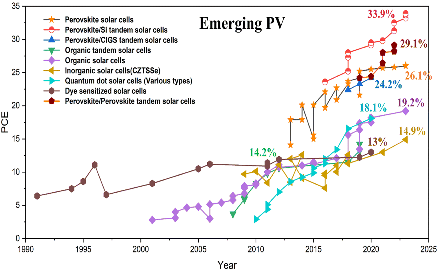 | ||
| Fig. 1 The recent progress of emerging photovoltaic solar cells. Data extracted from NREL (https://www.nrel.gov/). | ||
This rapid improvement implies significant progress in the photovoltaic industry. However, one of the key aspects influencing the performance and applicability of PSCs is stability, which determines their capability to sustain performance over time under various environmental conditions. Stability in PSCs is a multidimensional challenge. These PSCs are naturally vulnerable to moisture, oxygen, heat, and light, which can cause deterioration and loss of performance over time.10,14 Their performance and stability are also affected by crystal defects, ion migration, hysteresis and hydrophobicity.15–19 Band gap tuning through structural modification is a critical aspect of overcoming some of the aforementioned limitations and the optimization of PSCs for high performance and better stability. The band gap governs the range of energy of light that the perovskite materials can absorb efficiently. In an ideal world, the band gap should be modified to match the wavelength of solar energy to maximize light absorption and thus enhance the performance of the PSCs. The common techniques for band gap tuning in perovskite materials are compositional engineering, doping, interface engineering, dimensional modification, and pressure or strain.20–23 Fig. 2 shows the major approaches of band gap tuning towards the enhancement of the PCE of PSCs. By modulating the composition and structure of perovskite materials, researchers aim to modify their optical and electronic properties to achieve optimal performance from PSCs. In addition, by modifying the band gap, along with photovoltaic performance, stability against extrinsic and intrinsic degradation factors can be obtained.24,25
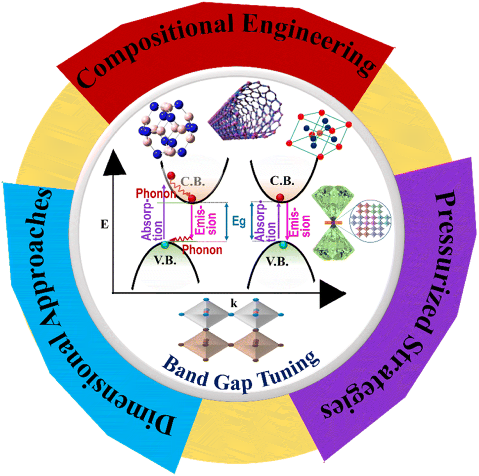 | ||
| Fig. 2 Major processes of band gap tuning towards the enhancement of the PCE of PSCs. | ||
This review extensively delves into the impact of band gap engineering on performance and stability, highlighting the influence and significance of cations, anion replacement in the perovskite structure, dimensional reduction and mixing of the dimensions, and pressure-induced bandgap modulation on material properties. By scrutinizing the structural changes and compositional variations, the review aims to provide a comprehensive understanding of how band gap engineering contributes to advancements in solar cell technology for achieving high performance and stability of PSCs. Specifically, this review makes it possible to comprehend the many tactics used in detail, as well as how well they work to improve the stability and performance of PSCs. It is expected that this review will open the door for a focused study to overcome the existing obstacles and constraints that still need to be addressed towards the maximum potential of perovskite solar cells, as it offers a critical appraisal of the existing level of knowledge.
2. Photon absorption management
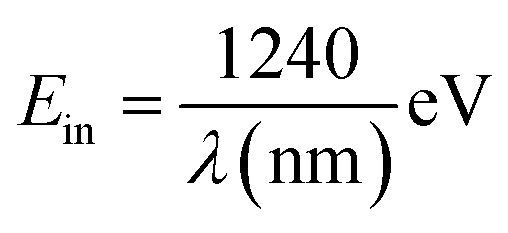
When photons interact with a semiconducting material, they can have three possible outcomes: (a) they may be reflected from the surface depending on the difference in refractive index between the material and surroundings, (b) they may be absorbed within the material depending on its extinction coefficient, or (c) it may be transmitted through the material. In the context of photovoltaic devices, both reflection and transmission are typically considered losses since photons are not absorbed and do not contribute to power generation. However, when a photon is absorbed, it can raise one electron from the valence band to the conduction band. The energy level of photons that will be absorbed can be estimated by using eqn (1):
 | (1) |
This band gap plays a crucial role in dictating which portion of the solar spectrum can be absorbed by a photovoltaic cell.26 A semiconductor will not absorb photons of lower energy than its band gap; a lower energy photon than the band gap energy will not be able to create enough excitation of the valence band electron to reach the conduction band. On the other hand, photons of higher energy than the band gap mostly generate heat by making a transition to the conduction band edge, offering no contribution to the solar cell's performance. For clearer comprehension, the incident photons can be fragmented into three categories based on their energy relative to the semiconductor band gap, and the absorption process is shown in Fig. 3.
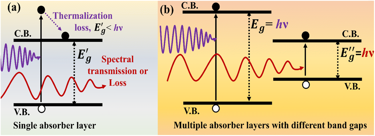 | ||
| Fig. 3 (a) Photon absorption and loss; (b) photon absorption management adopting multiple absorber layers with various band gaps. | ||
(a) If the incident photon energy Ein is smaller than the band gap energy Eg, only minimal interactions with the semiconductor will occur (and such an interaction will not contribute to the photovoltaic process) and will pass through the material as if it is transparent.
(b) For Ein = Eg, the incident photons have just enough energy to produce an electron–hole pair and consequently, the valence band electron can just reach the conduction band.
(c) If the incident photon energy Ein is larger than the band gap energy Eg, strong photon absorption occurs and the electron now stays on the conduction band with some excess energy. However, in photovoltaic applications, additional photon energy with respect to the band gap is lost by the quick non-radiative transition of electrons to the conduction band edge. This non-radiative transition leads to heat generation.
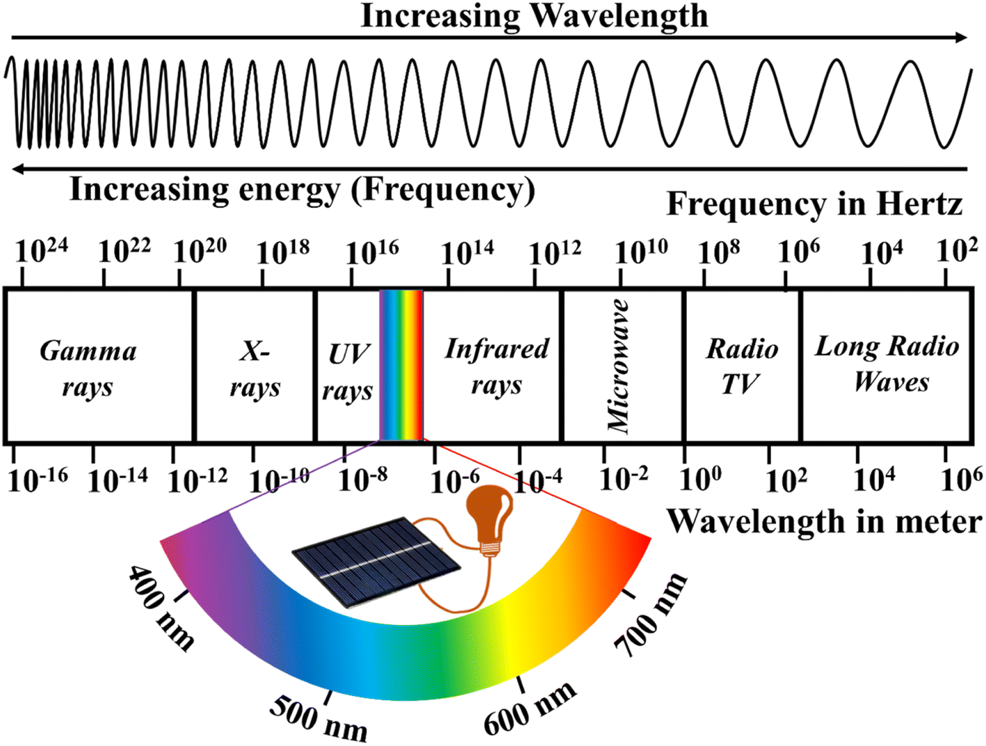
As an example, it is well known that the AM 1.5G sunlight has a wide range of useable energy from ∼0.5 eV to 4.4 eV (wavelengths from 280 nm to 2500 nm).27 The active perovskite materials used in PSCs typically have energy band gaps between 1.48 eV and 1.62 eV, where the optimum bandgap of the best-performing PSCs is almost pinpointed in the range from 1.53 eV to 1.56 eV.28–35 It has been reported that the PSCs with a bandgap of ∼1.5 eV can utilize incident photons in the 300–800 nm region and photon absorption over 800 nm has been reported to be less.21,27 This suggests that a significant portion of the solar energy over the near-infrared region cannot be utilized by the most recognized perovskites. The underutilization of high-energy photons is mainly related to hot carriers.
To address these issues, according to eqn (1), the photon management concept can be employed.39 This approach involves modifying the band gap to align with the solar visible spectrum (shown in Fig. 4), which can tune the absorption profile of the solar-sensitive material, thereby optimizing its performance. In addition, the band-gap fine-tuning optimizes semiconductors for use as bottom or top cell absorbers in PBTSCs for harnessing whole solar spectrum energy.40–42 Various research groups have implemented diverse approaches including compositional engineering, dimensionality reduction, mixing of dimensions, and pressurized tactics to modulate the band gap in materials to align them with the solar spectrum.20,21,43,44 These efforts have resulted in improved absorption, offering enhanced performance and heightened structural stability in solar energy conversion technologies.25
 | ||
| Fig. 4 Solar energy spectrum. | ||
Depending on the electronic band structure, there are two types of solar materials, namely, direct and indirect band-gap materials.45–47 The indirect band gap materials showcase weighty challenges when applied in solar cell applications. In contrast to direct band gap materials, where electron transitions occur without momentum modification, indirect band gap materials necessitate the participation of a phonon to conserve momentum during electronic transitions, as shown in Fig. 5.48,49 This additional requirement may meaningfully decrease the efficiency of photon absorption and the rate of electron–hole pair production, thereby controlling the performance of solar cells based on that material.50 Moreover, the phonon-assisted transitions launch additional non-radiative recombination corridors for the generated electron–hole pairs.51,52 These non-radiative routes can significantly degrade the overall performance of solar cells based on indirect band gap materials.53 Several research groups have undertaken initiatives to transform indirect band gaps into direct band gaps and adjust band structures to better match the solar spectrum.54 The goal of these efforts is to enhance the performance of solar energy conversion technologies by improving the absorption of sunlight and facilitating more efficient charge carrier generation.
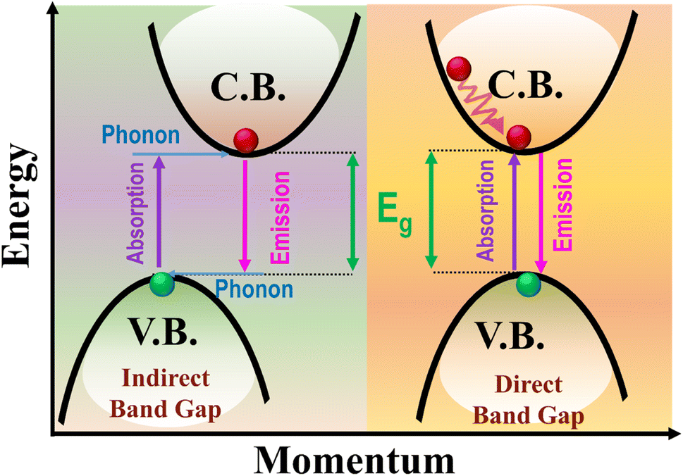 | ||
| Fig. 5 Absorption and emission in direct and indirect band gap semiconducting materials. | ||
3. Structural properties of perovskite materials
Perovskite is the term used to describe any ABX3 stoichiometric structure. This name originated from the discovery of CaTiO3 in 1839 by a German mineralogist Gustav Rose, who named it in honor of a Russian mineralogist Count Lev Alekseyevich von Perovski.55 In the ABX3 stoichiometric structure, A stands for a monovalent inorganic–organic cation, B represents a divalent metal cation and X denotes a halide anion.56 Furthermore, halogens can be replaced by oxygen, nitrogen, and carbon, etc. For example, A and B are often represented as divalent and tetravalent ions, respectively, when oxygen is utilized instead of halogen for charge neutrality.57 The cubic perovskite structure is comprised of corner-sharing BX6 octahedra, which form a 3D network with A-site cations in the 12-fold coordinated (cuboctahedral) vacancies to ensure charge neutrality (shown in Fig. 6).58,59 Conversely, the perovskite material may be viewed as a cubic close-packed AX3 sublattice with divalent B-site cations inside six-fold coordinated (octahedral) cavities.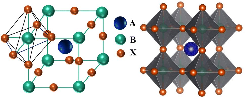 | ||
| Fig. 6 The basic structure of ABX3 with corner-sharing BX6 octahedral. | ||
The Goldschmidt tolerance factor is a dimensionless parameter and is used to predict the geometrical distortion and stability of perovskite structures based on the sizes of the cations and anions in ABX3. The Goldschmidt tolerance factor is defined by 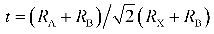 , where RA, RB and RX are the effective ionic radii for A, B, and X atoms respectively. It should be within the range of 0.80 < t < 1.0 to sustain the 3D structure.60 The tolerance factor of a given ABX3 not only serves as an indicator for evaluating its probability to adopt a 3D structure but also serves as a predictive tool for determining whether it will demonstrate a cubic phase (t ≈ 1) or deviate towards tetragonal (0.9 < t < 1.0), or tilted towards orthorhombic (0.8 < t < 0.9) phases.61 Additionally, non-perovskite structures form when the tolerance factor is larger than one or less than 0.8.62 Another crucial parameter known as the octahedral factor, μ, is used to forecast the formation of the BX6 octahedral and the stability of the perovskite structure. This factor is defined as the ratio of the ionic radius of the divalent cation RB to the ionic radius of the anion RX. This octahedral factor needs to be within the range of 0.414 < μ < 0.732 to facilitate the formation of the BX6 octahedral.63 Sustaining this 3D crystal structure is vital for easing the charge transport within the system, ensuring the efficient accumulation of photo-generated charges.64
3.1. The role of tolerance factors on phase stability
Crystal-structure changes can impact the stability of perovskite materials. A central measure for assessing the phase stability of perovskite structures is the Goldschmidt tolerance factor (t), which is based on the effective ionic radii of the elements in the ABX3 or mixed perovskite formula. In Section 3, it has been remarked that the tolerance factor should be in the range of 0.80 < t < 1.0 for a stable perovskite structure.60 In addition, tolerance factor values greater than 1 or less than 0.8 tend to result in non-photovoltaic perovskite structures. Fig. 7 shows the dependence of tolerance factors on the radius of the cation. According to Fig. 7, CsPbI3 and FAPbI3 perovskites are situated on the boundary of the perovskite region.65 It has also been observed that by adopting different size cations, tolerance factors can be balanced for a suitable range in photovoltaic applications.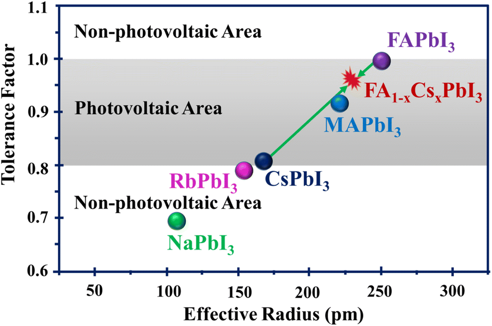 | ||
| Fig. 7 Correlations between the perovskite structure and the Goldschmidt tolerance factor. | ||
Depending on the tolerance factors, perovskite crystal phases can be categorized into cubic (t ≈ 1), tetragonal (0.9 < t < 1.0) and orthorhombic (0.8 < t < 0.9) structures. The α-phase of the perovskite structure is more stable than others. This phase has a cubic or tetragonal crystal structure, which is highly symmetrical and allows for effective charge transport. In comparison to the α-phase, the δ-phase exhibits less stability and symmetry. It does not have the desired perovskite structure and is frequently seen at lower temperatures. Its structure can drastically degrade the material's performance in devices such as solar cells since it doesn't allow charge movement as effectively. For example, there are two phases of FAPbI3, namely the photoactive α-phase with a large tolerance factor and the non-photoactive δ-phase. The δ-phase of FAPbI3 is converted to the stable perovskite α-phase at temperatures higher than room temperature.66 The impressive optical properties and record performance of MAPbI3 are overshadowed due to its phase instability.67 This material undergoes a structural shift from the tetragonal to cubic phase at 54–57 °C, which leads to various issues.68,69 These include the formation of defects, reduced mobility of charge carriers, shorter diffusion lengths, alterations in the band structure, and increased recombination losses within the absorbing material.70,71 An effective method to control phase stability is the balancing of the tolerance factors by compositional engineering. Some reports72,73 have suggested that the performance and the thermal/moisture stability of perovskites can be improved by adjusting the tolerance factors by adopting compositional engineering.
The prominent research group led by F. Valipour systematically investigated the influence of compositional engineering on performance and stability.74 They incorporated Cs+ into FAPbI3 and observed a change in tolerance factor along with phase. The introduction of Cs+ into the perovskite structure resulted in a reduction in the lattice constant and tolerance factor, consequently affecting the band gaps of the perovskite material by altering it from 1.47 eV to 1.53 eV for FAPbI3 to FA0.8Cs0.2PbI3 respectively. The XRD analysis demonstrated the elimination of non-photovoltaic phases and the transformation of the trigonal black phase into a tetragonal structure. Due to the introduction of Cs+ into FAPbI3, the transformation of the α-phase peak to higher 2θ values and the trigonal phase into a tetragonal phase reflects the decrease in the tolerance factor. The incorporation of 15% Cs+ led to notable enhancements, with the average efficiency reaching 7.41% and the highest efficiency peaking at 11.78% at high temperatures. In Fig. 8, the analysis of the XRD patterns of the pure FAPbI3 and the FA0.85Cs0.15PbI3 films showed that the peaks of PbI2 appeared after exposure to 150 °C temperature, which indicated the destruction of the perovskite film. However, more pinholes were observed in the FAPbI3 than in FA0.85Cs0.15PbI3 perovskite films. To compare the thermal stability of MAPbI3 and FA0.85Cs0.15PbI3 perovskite solar cells, both kinds were exposed to 120 °C over seven successive stages, each lasting 20 minutes. The J–V curves demonstrated that FA0.85Cs0.15PbI3 perovskite solar cells were more stable as compared to FAPbI3 and MAPbI3. The MAPbI3 perovskite exhibited a 50% decrease in performance after the first phase, whereas the FA0.85Cs0.15PbI3 perovskite showed a comparable loss after all seven steps of the test. To test moisture stability, samples were subjected to 90% humidity for 100 minutes and photovoltaic characteristics were assessed at 20 minutes intervals. The device with FA0.85Cs0.15PbI3 was more stable than FAPbI3, maintaining around 85% of its performance even after five steps. Thus, compositional engineering aids in achieving compatible tolerance factors for the structural stability of perovskites.
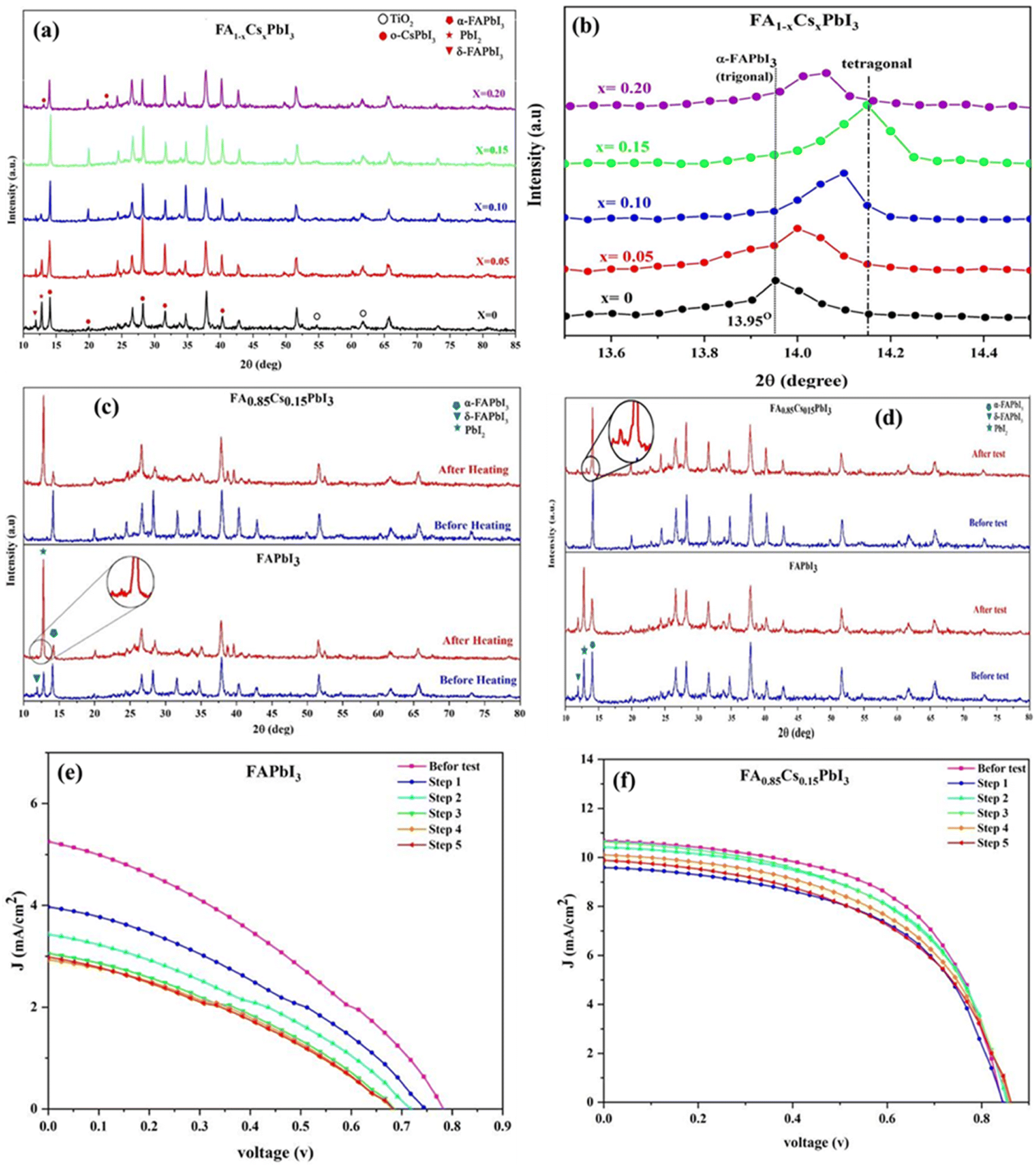 | ||
| Fig. 8 (a) The XRD outlines of the pure FAPbI3 and the Cs+-doped perovskite, and (b) the gradual shifting of the α-phase peak location toward higher 2θ values. (c) XRD analysis revealed the elimination of the yellow phase (δ-phase) after 100 minutes of heating at 150 °C. (d) Comparison of XRD patterns before and after the moisture stability test under 90% humidity. J–V curves during the moisture stability test: (e) FAPbI3 and (f) FA0.85Cs0.15PbI3. Reproduced from ref. 74 with permission from IOP Publishing Ltd, copyright 2020. | ||
4. Band-gap tuning
The band gap is the energy difference between the valence band maximum and the conduction band minimum of a material. Because of its direct influence on optoelectronic characteristics, band-gap adjustment in perovskite materials is crucial. It specifies the range of light wavelengths that a substance may absorb and convert into an electrical signal. The ability to modify the band-gap from low to high range has made perovskites appealing for a diversity of applications including photovoltaics, lasing, light-emitting devices, photodetectors, high energy, and particle detection.75 Metal halide perovskites are an encouraging family of materials for highly efficient PSCs for their tunable band-gap aligning with solar energy. In this section, compositional engineering, pressure-induced band gap modulation, and dimensional reduction and mixing approaches have been discussed.4.1. Compositional engineering
One of the most appealing aspects of perovskites for photovoltaics is the capability to adjust their energy band gap by simple compositional exchange. The perovskite semiconducting materials utilized in high-performing PSCs typically have energy band gaps between 1.48 eV and 1.62 eV.21,36–38 The semiconducting materials with lower band gaps are essential for capturing more of the visible solar spectrum. Utilizing different perovskite materials with varying band gaps enables the formation of PBTSCs, permitting the absorption of a wider spectrum of light. This approach has the potential to exceed the Shockley–Queisser PCE limit observed in single-junction PSCs.76 As an extensively used and high PCE-possessing material, the energy band-gap of methylammonium lead iodide (MAPbI3) may be adjusted from 1.6 eV to 2.3 eV by replacing iodine with bromine at different ratios.20 A similar technique may adjust the band gap of formamidinium lead tri-halide (FAPbX3) from 1.48 eV to 2.23 eV.21 The compositional band-gap fine-tuning optimizes metal halide perovskites for usage as bottom or top cell absorbers in tandem or single junction solar cells. A-site substitution has a relatively less direct impact on the edge of the band structure, i.e., Eg in comparison with B and X-site substitutions in the ABX3 phases.77 However, A-site cations can influence the lattice constant, which might indirectly influence the band structure. These A-site cations can also affect the dielectric characteristics, hydrogen bonding interactions (with halide anions), and/or alter the BX6 octahedral framework. We have outlined the following three factors involved with the compositional changes, which may facilitate the readers' understanding of the band gap engineering of the perovskite materials.(i) The first aspect is related to electronegativity, where Eg is increased when the electronegativity difference between the B-site metal and the X-site halide increases, but the A-site atoms have an indirect effect on Eg.78,79
(ii) The second factor linked to the Eg is the B–X–B angle. Particularly, Eg increases with the B–X–B angle decreases.80,81
(iii) The third factor is the distance between X and B atoms, where Eg is reduced as the distance between the X and B atoms decreases.78,82,83
In general, the influence of the B–X–B angle changes when the Eg tuning is greater than that of the inter-atomic distance. In a simplified manner, it can be asserted that the A-site replacement modifies the distance between the B-centered octahedrons by changing the lattice constant; however, it is anticipated that the B–X–B angle and B–X atomic distance will be relatively less affected by indirect lattice distortion. Only substituting halides does not offer a means to reduce the band-gap energy, especially below 1.48 eV. To attain lower band gaps, more effective strategies involve substituting A, and B cations, especially the B cations. For example, replacing lead cations on the B-site with tin may work as the most effective means for reducing the band-gap energy.84–86 Additionally, while the fractional replacement of halide allows for larger band gaps, several of these mixtures are not photo-stable and exhibit the Hoke effect (specifically in hybrid organic–inorganic perovskites), or segregate into Br-rich and I-rich domains when exposed to light.87,88 This phenomenon makes it challenging for high-band-gap semiconducting perovskite materials to get large open circuit voltage (Voc) in PSCs. Therefore, alternative band-gap tuning procedures are crucial for wide-ranging band-gap perovskite materials. It is essential to emphasize that when replacing atoms at various sites within the ABX3 structure, careful attention must be given to maintaining the Goldschmidt tolerance factor and octahedral factor in order to achieve and preserve the 3D crystal structure. It is generally well-known that the characteristics of a semiconducting material are substantially governed by its crystal structure; hence, geometric distortion considerably contributes to the modifications in the features of perovskite semiconducting materials. Various approaches for achieving high performance and stability of PSCs by band gap alteration are described in the following sub-sections.
 | ||
| Fig. 9 (a) Photovoltaic performance of the PSC with a configuration of FTO/c&m-TiO2/perovskite/spiro-OMeTAD/Au and (b) stability. Reproduced from ref. 101 with permission from Science, copyright 2016. | ||
Researchers have employed a strategy to heighten the stability and photovoltaic performance of perovskite materials by incorporating Bi into their structures. However, the performance is compromised due to less absorption of light, which is linked to their higher band gap. As an illustration, B. W. Park et al. developed two devices with the A3Bi2I9 structure by utilizing Cs and MA in the A-sites.102 They achieved band gaps of 2.2 eV and 2.1 eV, respectively, which exceed the energy range of the visible solar spectrum. The fabricated solar cells had the structure Ag/spiro-OMeTAD/A3Bi2I9/TiO2/FTO. The resulting PCE was 1.09% for Cs3Bi2I9 and 0.12% for MA3Bi2I9. The Sb-based solar cell, containing the A3Sb2I9 structure, revealed a similarly modest performance. Specifically, the devices incorporating Rb3Sb2I9 and MA3Sb2I9 demonstrated efficiencies of 0.66% and 0.49%, respectively, accompanied by relatively high band-gaps of 2.24 eV and 2.14 eV.103,104
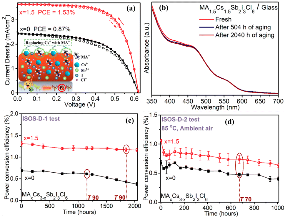
The renowned research team led by J. Xu successfully proved the efficacy of mixed-cation engineering by introducing both organic MA and inorganic Cs cations at the A-sites in mesoporous Sb-based PSCs.25 By changing the quantity of MA used to replace Cs cations at the A-site, they discovered an optimal composition, MA1.5Cs1.5Sb2I3Cl6, which had an equal amount of Cs and MA cations. Surprisingly, despite this modification, the band structure of the optimized material remained almost the same as pristine Cs3Sb2I3Cl6 (∼2.1 eV). This modified material displayed superior characteristics, allowing for enhanced light absorption, reduced series resistance (by a factor of 2.2), and increased shunt resistance (three times higher) as compared to the pristine structure. The configured PSC architecture was FTO/c&m-TiO2/MAxCs3−xSb2I3Cl6/spiro-OMeTAD/Au. The device with MA1.5Cs1.5Sb2I3Cl6 demonstrated an 81% boost in PCE as compared to single-cation devices (Cs3Sb2I3Cl6). Furthermore, the optimized mixed double-cation MA1.5Cs1.5Sb2I3Cl6 cells presented exceptional shelf-life, holding 90% of their initial PCE (1.53%) after 1800 hours of aging without light with a RH of about 30–55% with no encapsulation (a 60% improvement over the Cs3Sb2I3Cl6-based solar cell) and sustained 70% of their initial PCE after 650 hours of aging at 85 °C, demonstrating impressive thermal stability. The performance metrics are displayed in Fig. 10.
 | ||
| Fig. 10 (a) J–V curves for the reverse scan (solid line) and forward scan (dashed line) of the device FTO/c&m-TiO2/MAxCs3−xSb2I3Cl6/spiro-OMeTAD/Au. (b) Absorption spectra for the (a) Cs3Sb2I3Cl6 and (b) MA1.5Cs1.5Sb2I3Cl6 perovskite-inspired films. (c and d) Ambient and thermal stability tests for MAxCs3−xSb2I3Cl6 (x = 0 and 1.5) PSCs with no encapsulation. Reproduced from ref. 25 with permission from ACS, copyright 2024. | ||
The prominent research group led by Zhen Li studied the correlation between the perovskite crystal structure and the tolerance factor in lead halide perovskites, specifically FAPbI3 and CsPbI3.105 They observed that unfavorable yellow phases, such as δH-FAPbI3 and δO-CsPbI3, arise due to large and small tolerance factors, respectively. By the partial substitution of FA+ in FAPbI3 by Cs+ to tune the tolerance factor, the stabilization of the desirable α-phase in mixed perovskites was attained. They obtained 15% of Cs as the optimized amount and a 0.95 tolerance factor for improved performance and device stability as compared to their FAPbI3 counterparts. Adding Cs to FAPbI3 produced FA1−xCsxPbI3 compounds with lower δ-to-α phase transition temperatures as compared to pure FAPbI3 and CsPbI3. High humidity caused the α-to-δH phase transition in FAPbI3 films, but not in Cs-doped FA0.85Cs0.15PbI3 films, which reflects the significance of the tolerance factor on phase stability. The photovoltaic performance is tabulated in Table 1 and the graphical representation of the performance and stability of devices are depicted in Fig. 11.
| Compound | Jsc (mA cm−2) | Voc (volt) | FF (%) | PCE (%) | Band-gap (eV) |
|---|---|---|---|---|---|
| FAPbI3 | 19.69 | 1.06 | 68 | 14.2 | 1.47 |
| FA0.85Cs0.15PbI3 | 20.39 | 1.06 | 74 | 16.1 | 1.52 |
| FA0.70Cs0.30PbI3 | 19.46 | 1.04 | 73 | 14.8 | — |
| FA0.55Cs0.45PbI3 | 18.09 | 0.94 | 56 | 9.60 | — |
| FA0.30Cs0.70PbI3 | 18.08 | 1 | 56 | 10.2 | — |
| δO-CsPbI3 | 0.22 | 0.9 | 61 | 0.12 | 2.7 |
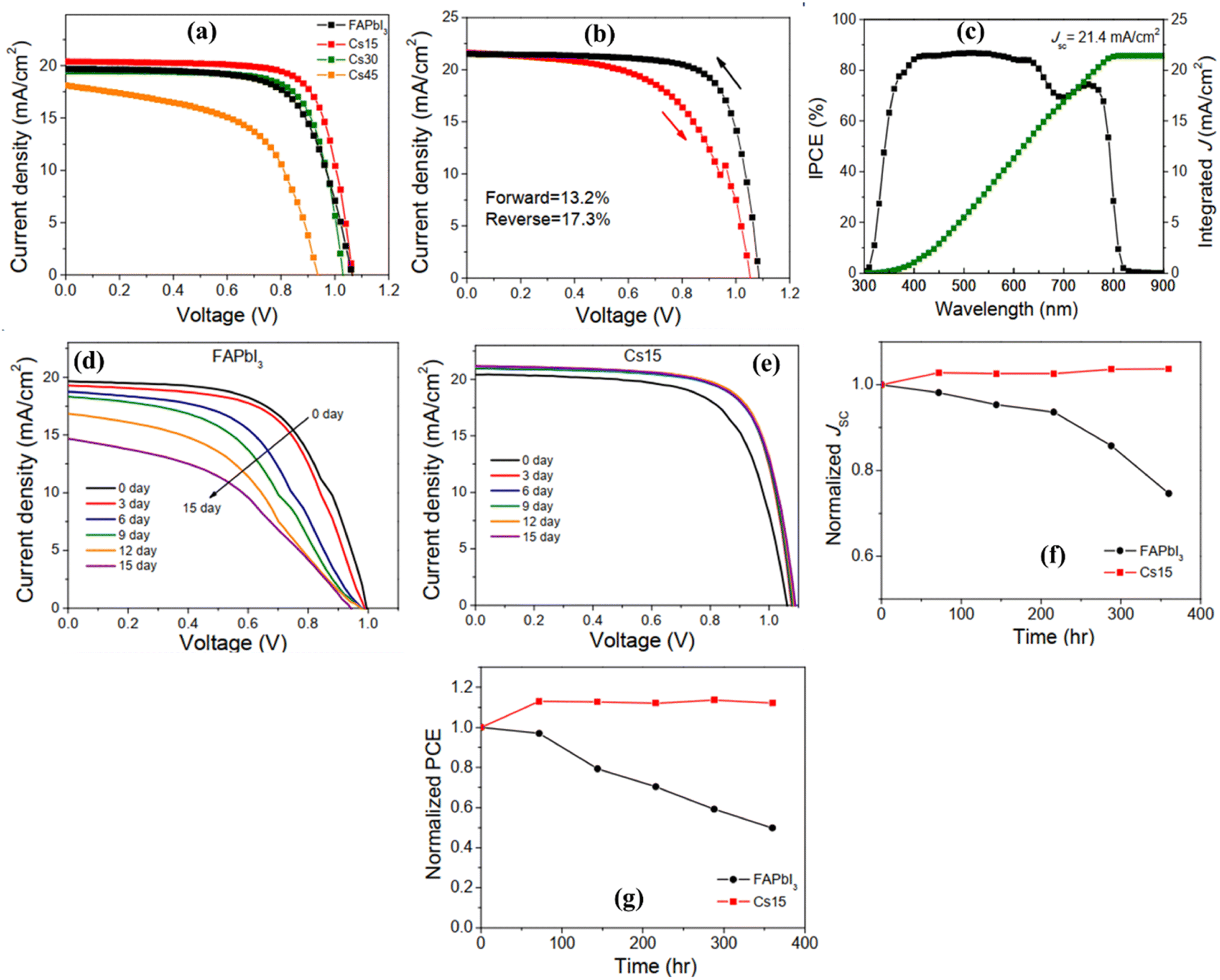 | ||
| Fig. 11 Photovoltaic parameters of FA1−xCsxPbI3-based solar cells. (a) J–V curves of FA1−xCsxPbI3-based solar cells with different concentrations of Cs+. (b) J–V curves of a champion device with composition FA0.85Cs0.15PbI3. (c) IPCE spectrum and the integrated photocurrent of the champion device. A comparison of the stability of FAPbI3 and FA0.85Cs0.15PbI3 solar cells. (d) J–V curves of FAPbI3 and (e) FA0.85Cs0.15PbI3 solar cells at 0–15 days of storage under 15% RH. Normalized (f) Jsc and (g) PCE of FAPbI3 and FA0.85Cs0.15PbI3 solar cells with different storage times. Reproduced from ref. 105 with permission from ACS, copyright 2016. | ||
:2Sn molar ratio have demonstrated promising efficiency, reaching 15.1%.112 It is necessary to note that Sn(II) shows lower chemical stability within an octahedral environment.113,114 The oxidation of Sn(II) to Sn(IV) has been associated with suboptimal performance and increased carrier concentrations in Sn halide perovskites. The distinguished research group comprised of Straus and Cava transformed the band-gap of CsPbBr3 by introducing Sr atoms at the B-site in place of Pb. By replacing as much as 75% of Pb with Sr, they attained a gradual increment in the band gap from 2.29 eV in pure CsPbBr3 to 2.64 eV in CsPb0.25Sr0.75Br3.115 In addition, the well-known research group led by N. Ito prepared a PSC using the FA0.75MA0.25Sn1−xGexI3 hybrid organic–inorganic structure. They adjusted the value of x from 0% to 20%, which led the band gap to shift from 1.40 eV to 1.53 eV. According to their findings, x = 0.05 (band-gap 1.4 eV) was the optimal value for the PSC with the structure ITO/PEDOT:PSS/FA0.75MA0.25Sn1−xGexI3/PCBM/C60/Ag. Their findings indicate that device performance was Voc = 0.42 V, short circuit current density (Jsc) = 19.50 mA cm−2, FF = 0.55%, PCE = 4.48%, Rs = 4.01 ohm cm−2, and Rsh = 227.96 ohm cm−2. It should be noted that the stability of the replacement of Pb by Ge(II) was further compromised due to its inferior binding energy associated with 4s2 electrons, which makes it an odd contender for solar materials. The prominent research group led by M. T. Klug delved into extensive band-gap engineering for the MAPbI3 material (initial band-gap of 1.56 eV) to optimize the performance of PSCs.100 The investigation discovered that the lattice structure of MAPbI3 displays remarkable tolerance to various extrinsic homo-valent species. The compositions, such as those involving Co, Cu, Sn, and Zn, were identified for enhancing photovoltaic performance without causing complete disruption. To be more specific, their systematic approach involved selectively substituting Pb with Co in MAPbI3. By varying the Co percentage from 0% to 6.3%, they effectively reformed the band structure and Fermi level without varying the material's band gap. The PSCs were constructed using the configuration Ag/BCP/PCBM/doped perovskite/spiro-OMeTAD/ITO. Precise performance metrics, especially PCE, were meticulously documented and presented in Table 2. Noteworthily, the device incorporating 1.6% of Co displayed the highest performance with a PCE of 17.2%, aligned with a corresponding band-gap of 1.56 eV.
| Co (%) | Pb (%) | Jsc (mA cm−2) | Voc (volt) | FF (%) | PCE (%) |
|---|---|---|---|---|---|
| 0 | 100 | 21.2 | 0.99 | 78.6 | 16.6 |
| 0.8 | 99.2 | 21.1 | 1.02 | 77.4 | 16.7 |
| 1.6 | 98.4 | 21.1 | 1.05 | 77.7 | 17.2 |
| 3.1 | 96.9 | 17.5 | 1.08 | 75.1 | 14.2 |
| 6.3 | 93.7 | 13.1 | 0.94 | 67.4 | 8.3 |
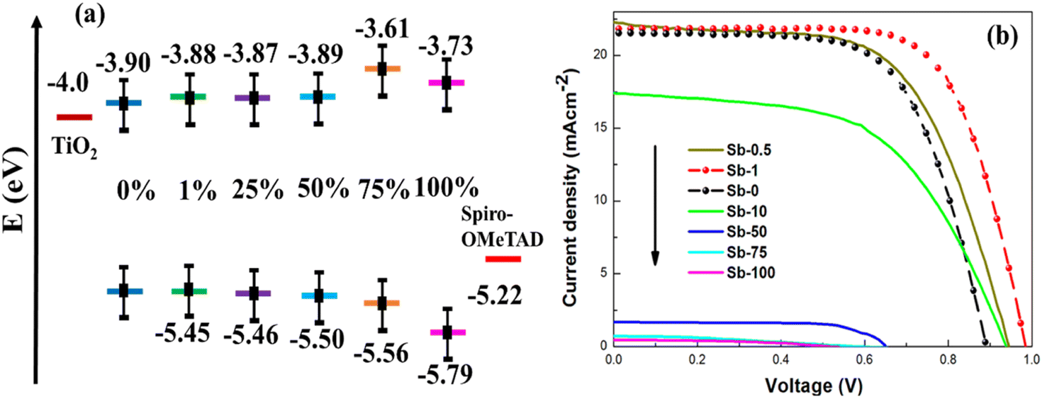
The renowned research group led by J. Zhang conducted an extensive investigation into band-gap engineering to optimize the PSC performance.116 Their tactic involved the systematic partial substitution of Pb with Sb in the MAPbI3 material. By changing the parameter x from 1% to 100% in the MAPb1−xSb2x/3I3 material, they efficiently modified the band gap from 1.55 eV to 2.06 eV. The PSCs were made up using the configuration FTO/TiO2/MAPb1−xSb2x/3I3/spiro-OMeTAD/Ag. The performance metrics, particularly in PCE, were precisely recorded and are presented in Table 3. Notably, the device with Sb-1% demonstrated the best performance with the highest PCE of 15.6% along with its corresponding band-gap of 1.57 eV. The performance metrics are revealed in Fig. 12.
| X (%) | Jsc (mA cm−2) | Voc (volt) | FF (%) | PCE (%) | Band-gap (eV) |
|---|---|---|---|---|---|
| 0 | 21.53 | 0.89 | 65.2 | 13.1 | 1.55 |
| 0.5 | 22.0 | 0.945 | 62 | 13.5 | — |
| 1 | 21.82 | 0.985 | 69.2 | 15.6 | 1.57 |
| 4 | 20.5 | 0.968 | 60 | 12.4 | — |
| 10 | 17.37 | 0.937 | 55.7 | 9.48 | — |
| 25 | 1.53 | 0.700 | 63.6 | 0.712 | 1.59 |
| 50 | 1.68 | 0.648 | 71.8 | 0.818 | 1.61 |
| 75 | 0.72 | 0.587 | 33.2 | 0.147 | 1.95 |
| 100 | 0.465 | 0.513 | 45.4 | 0.113 | 2.06 |
 | ||
| Fig. 12 (a) Band-gap modulation; (b) the influence of band-gap modulation on the photovoltaic performance metrics of the PSCs with MAPb1−xSb2x/3I3. Reproduced from ref. 116 with permission from ACS, copyright 2016. | ||
In double perovskites, the B-site undergoes substitution by two alio-valent ions, one with a higher oxidation state and another with a lower oxidation state. One obvious method is replacing Pb(II) with Bi(III), and Ag(I) with Tl(I), which is expected to lessen the electrical band gap. This reduction is ascribed to the inferior binding energy of Bi (6p orbitals) and the variations in electrostatic potential rising from the mixture of mono-valent and tri-valent ions.117 A notable benefit of this tactic is the capability to selectively influence n-type carrier concentrations (with excess Bi) or p-type carrier concentrations (with excess Ag, Tl) through controlled replacements beyond the 1:1 stoichiometry.
The well-known research team led by Y. Liu has demonstrated a bandgap modulation of Cs2AgBiBr6 by incorporating Sb to substitute Bi using a flexible solution-processing technique in dimethyl sulfoxide at a temperature of 180 °C.118 The resulting structures of Cs2AgSbxBi1−xBr6 (x = 0, 0.25, 0.50, 0.75) thin films displayed excellent crystallinity and thermal stability. Furthermore, the substitution of Sb led to an observable lessening in bandgap from 2.22 eV to 1.97 eV by 0.25 eV. Employing the Cs2AgSb0.25Bi0.75Br6 thin film in PSC fabrication with the configuration FTO/c&m-TiO2/Cs2AgSb0.25Bi0.75Br6/spiro-OMeTAD/Au resulted in improved performance as compared to the reference Cs2AgBiBr6. Specifically, the Cs2AgSb0.25Bi0.75Br6-based PSC showed significant enhancement over the Cs2AgBiBr6-based solar cell, with the average Voc increasing by 64% from 0.39 V to 0.64 V and PCE increasing by approximately 31% from 0.19% to 0.25%.
| Devices with perovskite materials | Jsc (mA cm−2) | Voc (volt) | FF (%) | PCE (%) | Band-gap (eV) |
|---|---|---|---|---|---|
| MAPbI3 | 17.45 | 0.977 | 61.13 | 10.64 | 1.56 |
| MAPb(I0.88Br0.12)3 | 13.89 | 0.890 | 65.31 | 8.13 | 1.62 |
| MAPb(I0.74Br0.26)3 | 10.39 | 0.936 | 61.95 | 6.13 | 1.69 |
| MAPb(I0.58Br0.42)3 | 8.20 | 0.898 | 65.84 | 4.63 | 1.79 |
| MAPb(I0.41Br0.59)3 | 6.35 | 0.834 | 52.40 | 2.80 | 1.96 |
| MAPb(I0.28Br0.72)3 | 3.18 | 0.940 | 48.54 | 1.39 | 2.01 |
| MAPb(I0.05Br0.95)3 | 2.38 | 0.832 | 49.81 | 1.03 | 2.23 |
The distinguished research team led by M. J. Wu developed PSCs by using a composition of MA0.85Cs0.15Pb(I1−xBrx)3 and explored their performance by substituting iodine with bromine at the X-site.122 The device configuration was ITO/PEDOT:PSS/perovskite/PC61BM/BCP/Ag. Their research revealed that the band gap varies as follows: 1.59 eV for x = 0, 1.66 eV for x = 0.15, 1.71 eV for x = 0.25, and 1.78 eV for x = 0.35. The most optimal performance was observed at x = 0.15, with reported photovoltaic parameters of Voc = 1.07 V, Jsc = 15.43 mA cm−2, FF = 61.76%, and PCE = 12.47%. The performance data of the devices are illustrated in both Fig. 13 and Table 5.
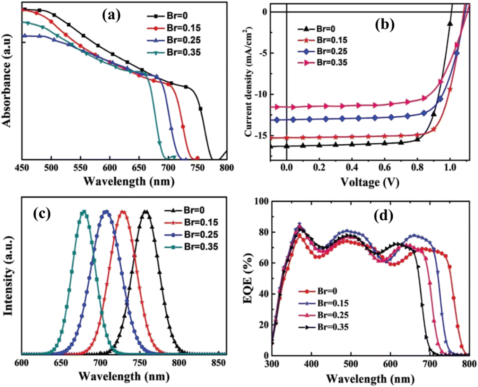 | ||
| Fig. 13 (a) Absorbance; (b) current density; (c) intensity and (d) quantum efficiency of the device with ITO/PEDOT:PSS/MA0.85Cs0.15Pb(I1−xBrx)3/PC61BM/BCP/Ag, measured under 1 sun conditions (100 mW cm−2, AM 1.5G). Reproduced from ref. 122 with permission from WILEY-VCH Verlag GmbH & Co. KGaA, Weinheim, copyright 2019. | ||
| Devices with perovskite materials | Jsc (mA cm−2) | Voc (volt) | FF (%) | PCE (%) | Band-gap (eV) |
|---|---|---|---|---|---|
| MA0.85Cs0.15PbI3 | 16.39 | 0.99 | 76 | 12.44 | 1.59 |
| MA0.85Cs0.15Pb(I0.85Br0.15)3 | 15.43 | 1.07 | 76 | 12.47 | 1.66 |
| MA0.85Cs0.15Pb(I0.75Br0.25)3 | 13.16 | 1.09 | 73 | 10.39 | 1.71 |
| MA0.85Cs0.15Pb(I0.65Br0.35)3 | 11.27 | 1.11 | 69 | 8.56 | 1.78 |
F. Hao and research team undertook a study focusing on band-gap tuning within the structure of MASnI3−xBrx to identify the optimal configuration for PSC applications.123 They methodically increased the Br content at the X-site and observed corresponding modifications in the band structure alongside photovoltaic performance. The most promising results were accomplished with the MASnIBr2 structure, which exhibited a PCE of 5.73% along with a band gap of 1.75 eV. Detailed performance metrics of other structures are provided in Table 6 and Fig. 14.
| Devices with perovskite materials | Jsc (mA cm−2) | Voc (volt) | FF (%) | PCE (%) | Band-gap (eV) |
|---|---|---|---|---|---|
| MASnI3 | 16.60 | 0.68 | 48 | 5.23 | 1.30 |
| MASnI2Br | 13.96 | 0.77 | 50 | 5.48 | 1.56 |
| MASnIBr2 | 11.73 | 0.82 | 57 | 5.73 | 1.75 |
| MASnBr3 | 7.93 | 0.88 | 59 | 4.27 | 2.15 |
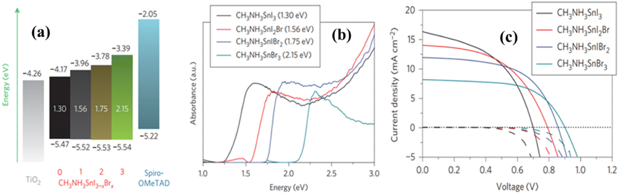 | ||
| Fig. 14 (a) Band-gap modulation; (b) absorbance; and (c) performance with respect to the variation of bromine in the X-site of MASn(I1−xBrx)3 perovskite. Reproduced from ref. 123 with permission from Springer Nature. Copyright 2014. | ||
The renowned research group led by J. Ma conducted an exploration into bandgap tuning within the CsPb(I1−xBrx)3 structure, where x varied from 0% to 66% (x = 0%, 20%, 33%, 50%, 66%), to optimize the structure for PSC applications.124 Their optimization efforts led them to identify the most suitable composition at x = 20%. By integrating chlorine into the structure, they revealed that the CsPb(I0.80Br0.20)3:Cl film exhibited the best performance. The PSC device developed with the configuration of ITO/ZnO/CsPb(I0.80Br0.20)3:Cl film/spiro-OMeTAD/Au accomplished notable results, including a PCE of 17.14%, a Voc of 1.21 V, a Jsc of 17.57 mA cm−2, and a FF of 80.36%. Z. Fang and colleagues pioneered the development of successful all-inorganic PSCs based on a 50–50% mixing halide approach in their groundbreaking work.125 Their approach utilized CsPbI1.5Br1.5 as the active material within the PSC structure, which was configured as Ag/MoO3/spiro-OMeTAD/SMH/perovskite/SnO2/ITO layers. Remarkably, the champion device combining SMH realized a remarkable PCE of 14.11%. This attainment represents the highest reported PCE to date for all inorganic CsPbI1.5Br1.5-based PSCs, representing the potential of their innovative design. Notably, even after 1000 hours of storage without encapsulation, the device sustained an impressive 85% of its initial efficiency, displaying not only high performance but also robust stability. Furthermore, H. Wang and his research team recently fabricated a PSC device utilizing mixed halide CsPbIBr2.126 Their efforts resulted in an impressive efficiency of 12.57%. Their exploration involved testing these PSCs under 1 m of water. Despite the challenging situations, they witnessed a minor degradation in the green and blue spectrum (400–600 nm) of the incident light. Nevertheless, the PSCs sustained a high PCE of 14.18%, exhibiting the robustness of their design even in underwater settings.
PBTSCs are a novel approach to photovoltaics that blends the unique features of perovskite materials with conventional solar cell technologies such as silicon and CIGS. In PBTSCs, two or more sub-cells with differing bandgaps are layered on top of one another, resulting in more efficient light absorption and higher PCEs than single-junction cells. A PBTSC normally consists of a bottom cell, which is commonly built from silicon/CIGS owing to its well-established technology and high efficiency, and a top or top and middle cell composed of a perovskite material. Sometimes all sub-cells can be made of perovskite materials. The perovskite materials have benefits such as adjustable bandgaps aligned with the solar spectrum, high absorption coefficients, and low-cost production processes, making them a good choice for PBTSCs.
Very recently, the eminent research group led by M. Heydarian developed a multi-absorber layer perovskite–perovskite–silicon tandem solar cell by adopting compositional engineering to adjust the band gaps of the top and middle cells made from perovskite materials in the tandem structure.127 In their design, the top perovskite absorber was Cs0.05(FA0.55MA0.45)0.95Pb(I0.55Br0.45)3 with a band gap of 1.83 eV. Meanwhile, the middle perovskite absorber was a triple-cation with a composition Cs0.05(FA0.9MA0.1)0.95Pb(I0.95Br0.05)3, which exhibited a band gap of 1.56 eV. The bottom cell consisted of a silicon heterojunction. Their champion cell accomplished a PCE of 20.1% with a FF of 78.1%, a Jsc of 8.9 mA cm−2, and a Voc of 2.87 V. These impressive structures demonstrate the potential of PBTSCs as a feasible technique for producing high-efficiency photovoltaic devices by combining the complementary light absorption capabilities of multiple materials with a suitable band gap inside the tandem structure. Recently, Wang et al. reported the development of the first certified all perovskite layer-based triple-junction PBTSCs.128 They modulated the band gap of the perovskite materials by compositional engineering. The three different perovskite absorbers were Rb0.15Cs0.85PbI1.75Br1.25 with a bandgap of 2.00 eV, Cs0.05FA0.90MA0.05Pb(I0.90Br0.10)3 with a bandgap of 1.60 eV, and Cs0.05FA0.70MA0.25Pb0.50Sn0.50I3 with 5% SnF2 with a bandgap of 1.22 eV. Their certified PBTSC exhibited remarkable performance metrics, including a PCE of 23.3%, a Jsc of 9.6 mA cm−2, a Voc of 3.20 V, and a fill FF of 76.2%. The encapsulated device confirmed excellent stability by retaining 80% of its original PCE after 450 hours of measurement in an ambient atmosphere. This groundbreaking accomplishment represents a significant advancement in the field of perovskite photovoltaics by demonstrating the viability of utilizing all perovskite materials in the PBTSC configurations with high efficiency and stability. Another research group formed by Isikgor and his co-workers developed a perovskite tandem solar cell where they utilized compositional engineering to modify the band gaps of the top cell and middle perovskite layers.129 Their modified perovskite absorber layers were Cs0.15MA0.15FA0.70Pb(I0.15Br0.85)3 with a band gap of 2.05 eV, and Cs0.15MA0.15FA0.70Pb(I0.85Br0.15)3 with a band gap of 1.62 eV. For the bottom cell, they used a ternary organic bulk heterojunction comprised of PM6:BTP-eC9:PC71BM with a band gap of 1.33 eV. Their PBTSC device with perovskite–perovskite–organic structure attained a PCE of 19.4%, with Voc of 3.03 V, a Jsc of 9.1 mA cm−2, and FF of 70.4%. The cell revealed satisfactory stability, as measured for 600 seconds at the maximum power point in a nitrogen environment.
4.2. Band-gap tuning by pressure
Pressure-driven bandgap engineering in perovskite materials is another potential approach for modifying their band-gap, which leads to manipulation of the optoelectronic characteristics.130 By subjecting perovskite structures to controlled external pressure, researchers can induce structural distortions and alter the electronic band structure. This phenomenon has important consequences in various applications, including photovoltaics, light-emitting diodes, and sensors. The capability to modulate the bandgap via pressure manipulation allows for the manufacture of perovskite devices with improved performance and stability over wide-ranging operating conditions. Understanding the multifaceted interactions between pressure-induced structural modifications and the consequent electrical features provides vital insights into the underlying physics of perovskite materials. As progress in both experimental approaches and theoretical modeling continues, pressure-driven bandgap engineering has shown enormous potential for opening new paths in the development of novel optoelectronic devices.To efficiently transform the bandgaps of perovskite materials, researchers usually apply satisfactory hydrostatic pressure using a diamond anvil cell (DAC). This approach is reasonable due to the relatively low bulk modulus of most perovskites in their ambient stages, typically under 30 GPa.131 Specifically, organic–inorganic hybrid perovskites like FAPbI3 have a bulk modulus of almost 14.66 GPa, which makes them particularly flexible to pressure-induced reform.22 Different findings on pressure-induced bandgap engineering in various perovskites provide several key points: firstly, high pressure can induce significant modifications in the band structure of perovskites, however, the exact behavior varies depending on the substance. Secondly, for most perovskites, changes in the bandgap occur continuously under pressure, which leads them to both blue shifts and red shifts in their absorption spectra.132,133 Lastly, high pressure often results in amorphization in perovskite crystals.134 Remarkably, this disorder is normally reversible upon decompression.131 Some representative works are revealed in Fig. 15.
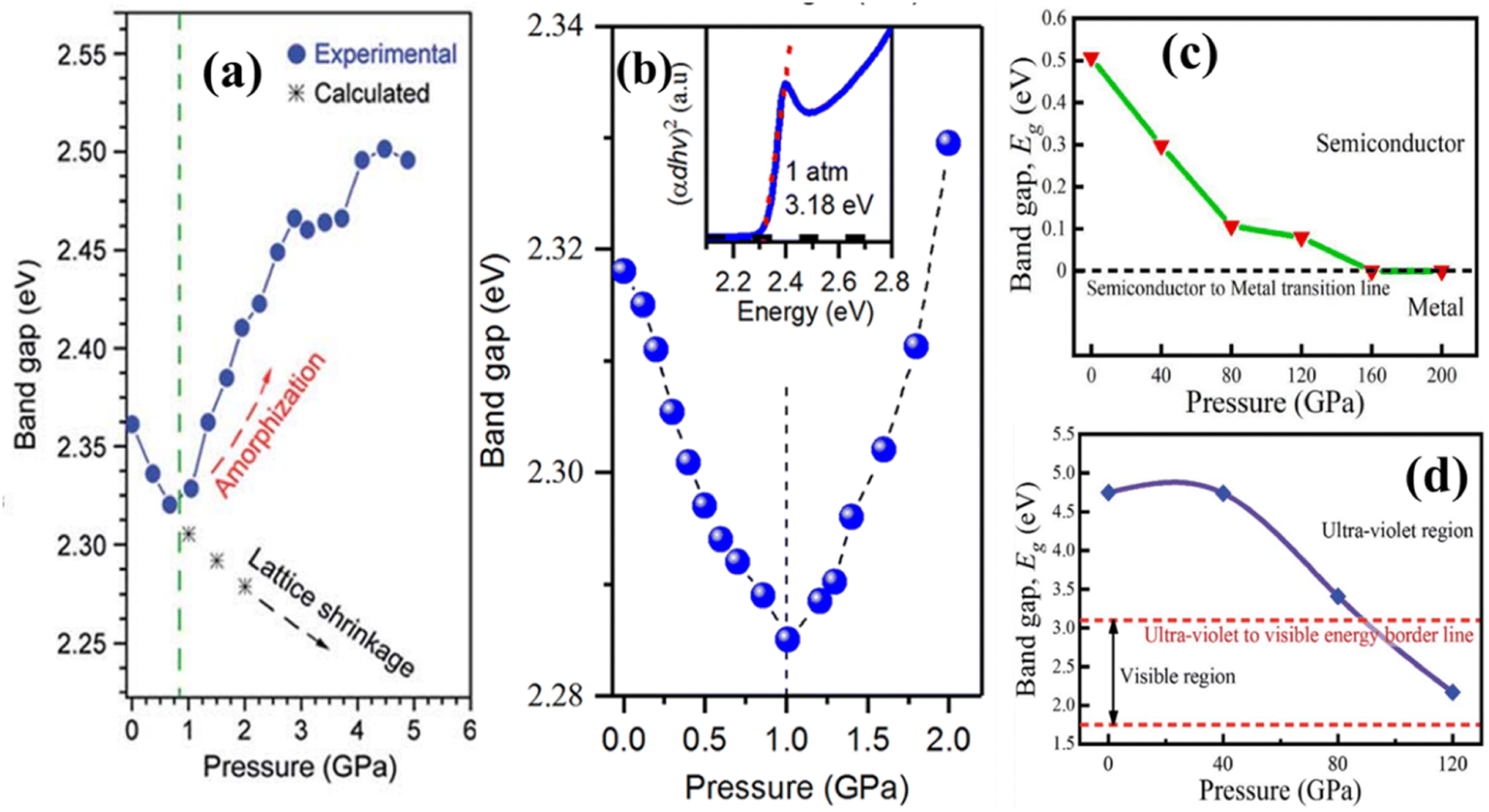 | ||
| Fig. 15 Pressure-induced band-gaps for MAPbBr3, CsPbBr3, CsYbCl3 and KCaCl3.135–138 (a) Reproduced from ref. 135 with permission from ACS. copyright 2015. (b) Reproduced from ref. 136 with permission from ACS. copyright 2017. (c) Reproduced from ref. 137 with permission from Elsevier, copyright 2022. (d) Reproduced from ref. 138 with permission from RSC, copyright 2021. | ||
The influence of cell volume on the semiconductor bandgap may be represented by the deformation potential αv, as shown in eqn (2).
 | (2) |
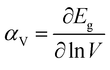
The renowned researcher H. Zhu and team conducted a comprehensive study on pressure-induced band-gap engineering.144 Their investigation inquired into the reasons behind the occurrence of red shifts, blue shifts, and amorphization under pressure. Their research focused on analyzing the optical properties of FAPbI3 perovskite materials under varying pressure conditions. Employing in situ absorption and photoluminescence measurements, they perceived a close relationship between changes in optical properties and pressure-driven phase transitions and amorphization of FAPbI3 nanocrystals. Initially, as pressure escalated from 0 to 2.3 GPa, both absorption and PL spectra exhibited continuous red shifts (PL spectra from 1.51 eV to 1.42 eV and absorption from 1.57 eV to 1.44 eV), which indicated a contraction of the Pb–I bonds and a consequential reduction of the band-gap due to increased orbital wave function overlap.145,146 However, after 5 GPa, further compression resulted in a blue shift in both the absorption band and the PL peak, as well as a significant fall in PL intensity caused by pressure-induced band-gap widening and the appearance of non-radiative relaxation pathways (deep intra-band trap states).147,148 During decompression, the absorption band continued to blue-shift until it reached 0.9 GPa and a broad PL peak emerged around 2.1 eV, indicating the onset of an amorphous phase in the FAPbI3 NCs. The genesis of this amorphous state in PL is unknown but it is likely linked to a short-range order of strongly tilted [PbI6]4− octahedra inside the amorphous FAPbI3 NCs. Releasing pressure below 1.0 GPa alleviates strain on the NC surface, resulting in fewer defects and shallower surface-related exciton trap states, which leads to enhanced emission from the amorphous state.149–151 Upon further pressure release, reversible red shifts were witnessed in both the absorption and PL spectra, with the PL peak center reverting to its initial position of 1.56 eV once pressure was totally removed. Although the compression typically increases charge carrier lifetime in most perovskite crystals by reducing shallow defect states in the vicinity of the valence band maximum, the atomic distortion owing to the mismatch among the crystal constants of perovskite films and substrates can generate additional defects, resulting in a significant increase in non-radiative carrier recombination.142 They also reported the carrier life by analyzing PL data. The PL profile displayed a higher energy level (approximately 50 meV), a wider linewidth (around 100% broader), and shorter-lived charge carriers (with a lifetime of 57.0 compared to 79.1 ns) compared to the initial PL of the FAPbI3 nanocrystals before pressurization (shown in Fig. 16). These findings can be attributed to the reduced crystallinity, less organized surface atoms, and the presence of ligand states in the final nanocrystals following pressure treatment.
 | ||
| Fig. 16 (A) Snapshots of FAPbI3 NCs in a DAC at various pressures. (B) Absorption and (C) PL spectra under pressure. (D) PL peak intensity evolution before complete amorphization. (E) PL peak position evolution before complete amorphization. (F) PL lifetime decay curves of the FAPbI3 NCs before and after pressure. Reproduced from ref. 144 with permission from ACS, copyright 2018. | ||
The pressure-induced transitions from indirect to direct bandgaps represent an alternative method applicable to semiconductors.152–154 Different research groups theoretically investigated how indirect band-gaps are transformed into direct band-gaps.43,155–157 For example, M. A. Haq et al. conducted a theoretical study on KCaCl3 perovskite materials, revealing that under 120 GPa, the indirect bandgap was transformed into a direct one by reducing its band-gap from 4.75 eV to 2.17 eV.43 Although the hybrid perovskite MAPbI3 is typically considered a direct bandgap semiconductor, it has been confirmed to retain a slightly indirect bandgap nearly 60 meV below the direct gap. This slight indirectness arises from the Rashba-splitting of the conduction band induced by the local electric field produced due to the deficiency of inversion symmetry around the lead site. Pressure can change the Pb framework structure, which is governed by the order of MA cations in the tetragonal phase. Wang et al. applied pressure exceeding 325 MPa to modify the Pb framework structure, transitioning the somewhat indirect bandgap into a highly direct one.158 This resulted in a nearly 30 meV redshift in the bandgap under 325 MPa pressure. However, this alteration was reversible even after the phase change, indicating the process's reversibility. Additionally, pressures higher than 325 MPa for MAPbI3 led to bandgap widening. Furthermore, there is limited experimental data on the effects of applied pressure on the position of the valence band maximum and conduction band minimum in the k-space for perovskites, necessitating further investigation to understand the potential indirect-to-direct transition. This is because the features observed under high pressure are typically reversible upon decompression. As a result, when using this approach in photovoltaics, substrates with matching crystal constants and moduli are required. The complete device may need to be stored at high pressure to retain its performance.
4.3. Band-gap tuning by reducing dimension
Reducing the dimensionality of perovskite materials has enormous potential for bandgap engineering, which leads to altering their electrical and optical characteristics.23 Quantum confinement effects become more prominent when perovskite structures are limited to two, one or even zero dimensions, resulting in tunable bandgaps and distinctive electrical characteristics.159 Quantum dots, nanowires, and 2D perovskite layers have size and thickness-dependent bandgaps, which allows for fine control over light absorption and emission spectra.160 The capability to modify the bandgap of the perovskite via dimensionality reduction opens up new possibilities for applications comprising solar cells, photodetectors, and LED, where precise control of optical and electronic properties is critical for device performance.In perovskite structures, the normal 3D framework is disrupted if the A-site cation is larger in comparison to the optimal size required by the tolerance factor.161 This size mismatch results in the formation of a 2D layered structure, where the large A-site cation acts as a spacer and divides the crystal along a specific direction. The octahedral BX64− units provide inorganic layers that alternate with layers of bigger organic cations in this modified 2D structure. The electrostatic forces hold these layers together and ensure a stable 2D perovskite structure.89 The existence of massive organic ions in the structure of 2D layered perovskites improves their stability. Even though these bulky cation layers might inhibit carrier transportation within the 2D layer, these layers play an important role in modulating the electrostatic forces acting on electron–hole pairs. Due to both quantum and dielectric confinement effects, the layered perovskites possess high exciton binding energy.162 In these 2D structures, the organic cation layers that function as dielectric spacers are mentioned as barriers while the semiconductor inorganic layers comprising numerous perovskite plates are denoted as wells.163,164 The dielectric confinement is developed inside the 2D structure due to the difference in dielectric constants between barriers and wells.161,162 The band gaps of these materials are influenced by the 2D confinement effect and vary with the number of perovskite layers (n), which is crucial for their optical properties.165 The electronic structure of various quantum wells is produced by alternating organic and inorganic layers with variable formation energies.166,167 The exciton binding energy in 3D perovskites is substantially lower than in quasi-2D perovskites, which has a substantial impact on exciton dissociation in electric fields.168 The massive organic cations in the insulating interlayer control charge transportation among the inorganic layers, which leads to limited carrier mobility and a relatively high band gap; therefore the performance of quasi-2D PSCs remains poor.169 The transportation mechanism is deeply dependent on electronic coupling between nearby quantum wells, hence modifying spacer cations is an effective way to enhance carrier transportation in 2D perovskites for efficient PSCs.
Researchers are investigating the 2D–3D mixed perovskite heterojunctions to address the issue of instability in 3D perovskites while making use of their inherent high efficiency. This approach assimilates the strengths of both 2D and 3D perovskites, in which the 3D component ensures efficient absorption across a broad spectrum of light, and the 2D structure enhances the longevity of PSCs in harsh environments.161 Picking the right organic cations to form mixed 2D–3D perovskites is essential for making the compatible energy level alignment between the perovskite and the charge transport layers for enhancing charge transportation through layers. With illumination by sunlight, the perovskite layer produces charge carriers that move towards the electrodes and establish a current in the external circuit. The efficient transportation of electron–holes at these interfaces strongly depends on how well the alignment of the energy levels at these interfaces match. This matching directly impacts the efficiency of charge collection and consequently influences the overall PCE of the devices. According to various reports, the inclusion of a 2D perovskite layer can expand the band gap at the interface of a 3D perovskite and thus fine-tuning of the energy levels can be done. Moreover, a thin 2D capping layer can inhibit electron recombination by putting its conduction band energy lower than that of the 3D. The research group led by Ma reported that a 2D capping layer containing conjugated cations improves carrier extraction efficiency due to better energy level matching.170 Furthermore, increasing the maximum valence band on the cation surface through multifunctional capping layer modifications substantially lowers the energy disparity between the perovskite and the HTL. This reduction decreases the barrier for hole extraction at the interface of the HTL/perovskite, which significantly boosts the hole extraction efficiency. Thus, cations with conjugated structures are frequently chosen to adjust the energy level matching in 2D–3D mixed PSCs. Large organic cations on the surface may migrate into the bulk perovskite film, where a gradient distribution of 2D perovskites is formed inside the 3D structure. This gradient can lead to a gradual narrowing of the bandgap as it approaches the bulk perovskite and forms a smooth energy level gradient rather than a linear change. This alignment reduces surface recombination and boosts the open-circuit voltage of the PSCs.171
Grain boundaries and surfaces within 3D perovskites assist as the primary pathways for ion migration. Additionally, ion migration at interfaces between the perovskite and carrier transport layers can initiate irreversible chemical reactions with the charge transfer layer or metal electrode that can lead to the degradation of the device. For instance, the migration of I− ions from the bulk perovskite to the HTL interface can cause an irreversible chemical reaction with the oxidized spiro-OMeTAD+ to form the neutral spiro-OMeTAD-iodine. The formation of the conjugated spiro-OMeTAD-iodine gradually reduces the conductivity of HTL. Furthermore, mobile I-ions can react not only with organic HTL but also with metal electrodes even in well-sealed devices, which leads to corrosion. Fortuitously, research has confirmed that the incorporation of a 2D perovskite layer with large organic ligands into a 3D perovskite can reduce cross-layer ion migration in PSCs.172,173 The well-known research team of Chen et al. found that the inclusion of a 2D perovskite layer in a 3D perovskite layer can minimize ion migration by introducing fluorine atoms into the benzene structure.174 This stimulates parallel π interaction and decreases ion migration. Moreover, the formation of 2D perovskites at the grain boundaries of 3D perovskites can effectively passivate ion diffusion channels by boosting the potential barrier for I-ion migration and hindering migration to both the hole transport layer and the metal electrode. This greatly improves the internal stability of perovskite solar cells.
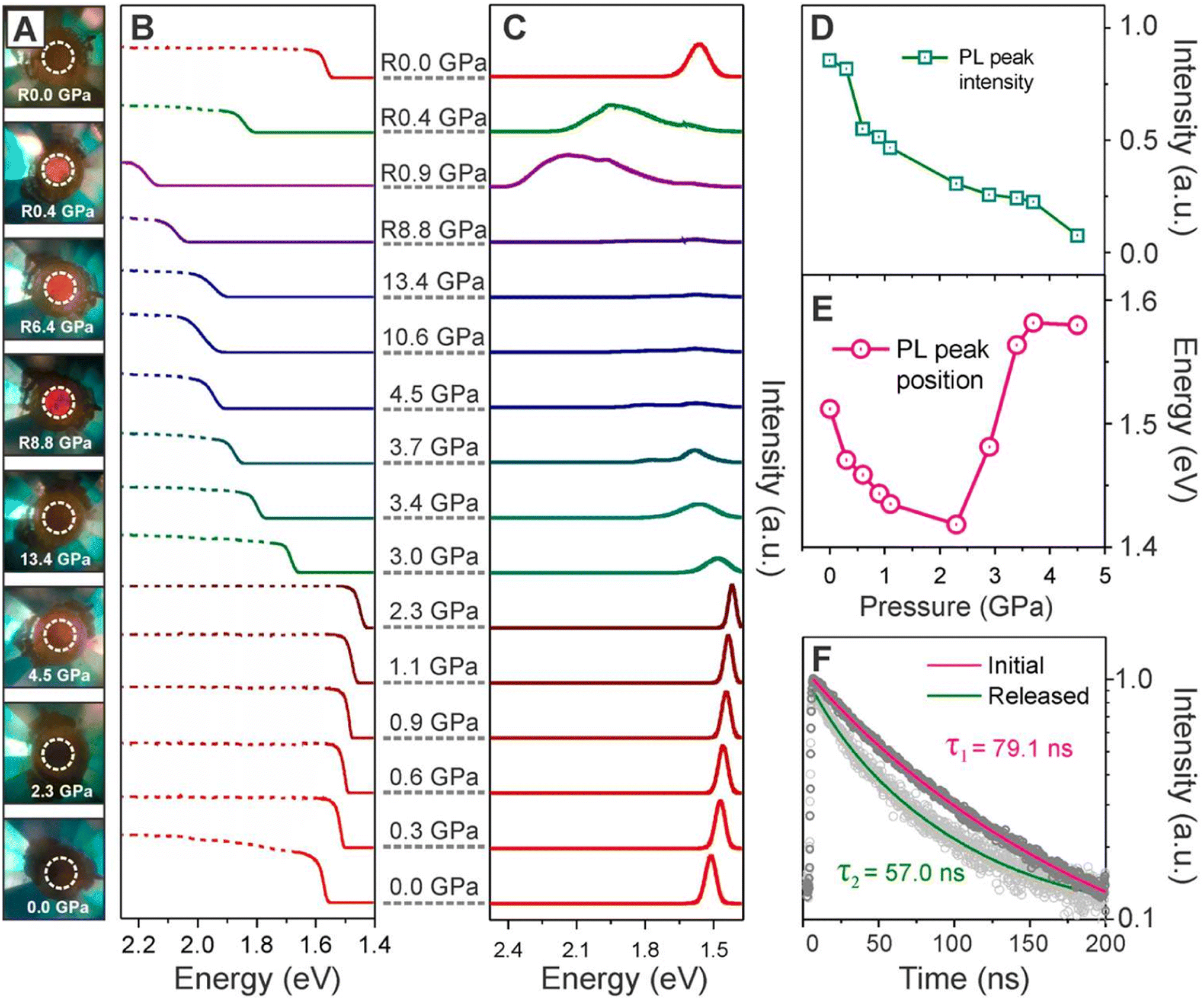
The quantum confinement effect causes a low-dimensional perovskite's bandgap energy to rise relative to its bulk equivalent. This is followed by altering the geometrical size of perovskite nanostructures, which will further modify the bandgap. As demonstrated in Fig. 17(a and b), PL emission wavelengths were continually modified by gradually reducing the size of FAPbI3 NCs (7.5–13 nm edge length). The estimated bandgap energy was enlarged from 1.5 eV in the bulk to over 1.7 eV for perovskite NCs with ∼8 nm edge length.175 Different researchers also confirmed a wide modulation in the bandgap of the representative MAPbX3, CsPbI3, and CsPbBr3 NCs and quantum dots.176–179 The 2D perovskites that have recently attracted much study interest have several distinct optical and electrical features compared to the bulk perovskites and other 2D materials.180–183 2D perovskites use ionic bonding in their crystal lattice, whereas inorganic 2D materials like TMDCs use covalent bonds. Organic molecules sandwiching a 2D hybrid perovskite crystal plane provide extra functionality, including the ability to alter the quantum well shape by adjusting the length and type of the organic chains.184–186 Fig. 17(c) demonstrates the layer number-dependent PL spectra of 2D BA2(MA)n−1PbnI3n+1 perovskites. These perovskites have a significant wavelength fine-tuning range of ∼520 nm to 650 nm (<130 nm difference, corresponding to a ∼0.47 eV shift).187 In another study, it was found that the bandgap energy gradually decreases with increasing layers in 2D perovskites with organic (MA, PEA) and inorganic (Cs) cations, as shown in Fig. 17(d). The energy difference between one unit cell and five unit cell crystals reached ∼0.6 eV.44
 | ||
| Fig. 17 Bandgap engineering by modifying the dimensionality. (a) Size-dependent PL spectra of FAPbI3 NCs. (b) Bandgap versus edge length of FAPbI3 NCs. Reproduced from ref. 175 with permission from Springer Nature, copyright 2018. (c) PL spectra of exfoliated monolayers for 2D BA2(MA)n−1PbnI3n+1 Ruddlesden–Popper perovskites of n = 1 to 4 homologues. Reproduced from ref. 187 with permission from Springer Nature, copyright 2018. (d) The bandgap of PEA2A1.5Pb2.5Br8.5 (A = MA and Cs) perovskites with different numbers of layers. Reproduced from ref. 44 with permission from Springer Nature, copyright 2018. | ||
The prominent research group led by Y. Xia successfully made a thermally stable quasi-2D perovskite by employing 3-(trifluoromethyl)benzylammonium iodide (3-TFMBAI) as a novel fluorinated spacer in Cs0.17FA0.83Pb(I0.83Br0.17)3.24 By integrating 3-TFMBAI, researchers were able to form molecular planes with significant hydrophobic characteristics, thereby protecting the perovskite phase from hydrolysis and degradation in ambient air. Furthermore, the introduction of 3-TFMBAI spacers promoted the formation of the Ruddlesden–Popper perovskite phase with quantum well structures, allowing trap states to be passivated and ionic mobility to be inhibited inside the perovskite lattice. Additionally, the inclusion of Cs+ ions enhanced the bandgap and improved the thermal stability of the resulting perovskite sheets. The resultant (3-TFMBA)2(Cs0.17FA0.83)n−1Pbn(I0.83Br0.17)3n−1I2 layer showed different band-gaps with respect to the variation of n, which are shown in Fig. 18. The champion devices, (3-TFMBA)2(Cs0.17FA0.83)n−1Pbn(I0.83Br0.17)3n−1I2-based PSCs, have an extraordinary PCE of 20.89% and a high Voc of 1.22 V at n = 40. Notably, these quasi-2D PSCs without encapsulation revealed amazing thermal and moisture durability, retaining 90.7% of their initial PCE even after 1000 hours of continuous exposure to 60 °C and 60% RH.
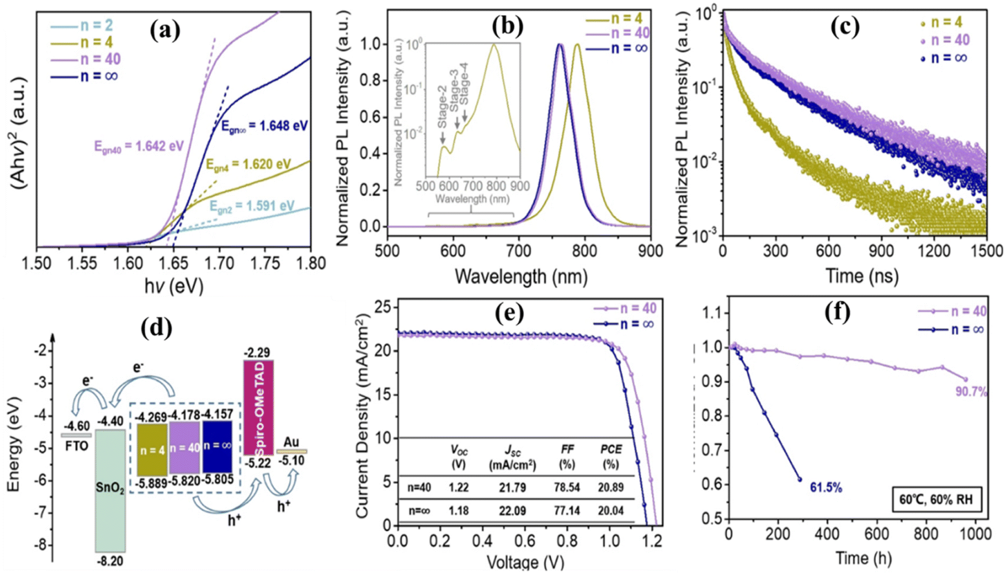 | ||
| Fig. 18 Film properties: (a) (Ahν)2 vs. hν curves, (b) steady PL spectra, and (c) TRPL spectra of (3-TFMBA)2(Cs0.17FA0.83)n−1Pbn(I0.83Br0.17)3n−1I2 perovskite films. Device performance: (d) The corresponding energy level alignment diagrams of glass/FTO/SnO2/perovskite/spiro-OMeTAD/Au. (e) Typical J–V plots: (f) Normalized PCE retentions of different PSCs with no encapsulation under continuous heating at 60 °C and simultaneous exposure to an RH of 60%. Reproduced from ref. 24 with permission from Elsevier, copyright 2023. | ||
In a recent study, H. Jiao et al. introduced a molecule known as tributyl(methyl)phosphonium iodide (TPI) into the FA0.91Cs0.09PbI3 perovskite precursor solution, which has the remarkable ability to transform conventional perovskite materials into 1D highly stable, mechanically robust, and water-insoluble forms.188 When TPI was combined with the perovskite precursor solution, the researchers noticed a novel grain-wrapping behavior during the perovskite film development. This wrapping efficiently turned both grain surfaces and boundaries into thin 1D TPPbI3, increasing moisture resistance and lowering iodine leakage under light exposure. The resultant perovskite films with wrapped grains exhibited outstanding stability under a variety of stressors including heat, light, and moisture. Surprisingly, the best-performing device retained 92.2% of its peak PCE even after 1900 hours of exposure to 1-sun illumination at 55 °C. Furthermore, the grain wrapping method considerably decreased iodide-related defect production, resulting in higher stability and performance. Specifically, the devices made utilizing this method attained a PCE of 22.9% along with a Voc of 1.150 V, Jsc of 24.70 mA cm−2 and FF of 81%, and maintained an 80% efficiency even after 3783 hours of light soaking.
The well-known research group formed by B. Zhao et al. introduced a novel approach to interface modification in PSCs by focusing on the utilization of fluorinated CsPbI3 perovskite quantum dots (PQDs).189 They also modified CsPbI3 PQDs by adding perfluorooctanoic acid (optimal 20% molar ratio) with oleic acid, designated as F–CsPbI3 PQDs. These F–CsPbI3 PQDs demonstrated superior performance compared to the traditional oleic acid (OLA)/oleylamine (OAm) ligand-capped PQDs due to their enhanced binding affinity and hydrophobic nature. The synthesis process of F–CsPbI3 PQDs involves optimization to reduce surface defect states, enhance PL quantum yields, and improve stability. Both CsPbI3 PQDs and F–CsPbI3 PQDs serve as interface engineering layers in n-i-p PSCs with the mixed Cs0.05FA0.85MA0.10Pb(I0.90Br0.10)3 perovskite absorber. The devices incorporating F–CsPbI3 PQDs achieved a significantly higher efficiency of 23.42% compared to the control devices with CsPbI3 PQD (21.99%) and 3D CsPbI3 (20.37%). Moreover, the F–CsPbI3 PQD-based devices revealed outstanding ambient storage stability, holding over 80% of their initial PCE after 1500 hours of aging at 25 °C and an RH of 35–45%. Recently, H. Liu and colleagues successfully introduced 0D-Cs4Pb(IBr)6 into 3D CsPbI3−xBrx perovskite films, forming mixed-dimensional structures of 0D–3D.190 This was attained by integrating excess n-CsBr into the precursor solution at low temperatures (120 °C). The incorporation of Cs4Pb(IBr)6 boosted the crystallinity of the CsPbI3−xBrx film and passivated grain boundary defects, which offered increased photovoltaic performance of the all-inorganic perovskite. In addition, the inclusion of Cs4Pb(IBr)6 perovskites converted tensile stress into compressive stress in the perovskite film, successfully preventing crack expansion and significantly enhancing the mechanical ductility of CsPbI3−xBrx PSCs. Due to the addition of different amounts of CsBr to the solution, the band-gaps of the 3D structure were changed as follows: 2.710 eV for CsPbI3 (0 M CsBr), 1.771 eV for CsPbI2.93Br0.07 (0.3 M CsBr), 1.788 eV for CsPbI2.81Br0.190 (0.5 M CsBr), and 1.801 eV for CsPbI2.72Br0.280 (0.7 M CsBr). Among these, the CsPbI2.81Br0.19-based PSCs achieved the highest PCE of 14.25% with a Jsc of 18.47 mA cm−2, Voc of 1.09 V, and FF of 70.67%. The fabricated devices confirmed excellent mechanical durability, holding over 97% of their original PCE, even after 60000 bending cycles at a radius of curvature R = 5 mm. For bending cycles of R = 3 mm, the devices sustained over 97% of their original PCE after 15000 cycles, underlining exceptional mechanical robustness. The incorporation of all-inorganic lower-dimensional perovskites excellently enhanced the bending durability of the PSCs, suggesting a promising avenue for enhancing the mechanical durability of all-inorganic PSCs. The photovoltaic performance metrics are presented in Table 7.
| Concentration of CsBr (M) | Device with perovskite materials | Jsc (mA cm−2) | Voc (volt) | FF (%) | PCE (%) | Band-gap (eV) |
|---|---|---|---|---|---|---|
| 0 | Cs4Pb(IBr)6/CsPbI3 | 11.12 | 0.76 | 52.91 | 4.48 | 2.710 |
| 0.3 | Cs4Pb(IBr)6/CsPbI2.93Br0.07 | 15.96 | 1.06 | 59.67 | 10.12 | 1.771 |
| 0.5 | Cs4Pb(IBr)6/CsPbI2.81Br0.190 | 18.47 | 1.09 | 70.67 | 14.25 | 1.788 |
| 0.7 | Cs4Pb(IBr)6/CsPbI2.72Br0.280 | 15.88 | 0.99 | 59.81 | 9.41 | 1.801 |
5. Relative discussion on various approaches to band gap tuning
This review investigates the various methods for modifying the band gap to better utilize the solar energy spectrum. It discusses compositional engineering, dimensional approaches including dimension reduction and mixing dimensions, and pressure-induced band gap modification. Compositional engineering involves replacing elements in different sites in ABX3, where B and X-site modifications have more pronounced effects on the electronic band gap structure as compared to A-site replacement. While A-site replacements mainly influence the spatial arrangement of octahedral structures, B and X-site replacements directly impact the conduction and valence bands of the perovskite materials, respectively. Consequently, strategies focusing on B and X-site modifications are more effective for attaining desired band gap adjustments. One of the renowned research groups efficiently modified the band gap and power PCE of MAPbI3 by swapping lead cations with antimony.116 They systematically varied the amount of inserted antimony and observed a significant 33% modification in band gap and 99% variation in PCE with complete substitution of Pb by Sb. This highlights the substantial influence of B-site replacements on the electronic band structure and performance metrics. One prominent research group attained improved efficiency of 14.1% and stability by mixing halides at the X-site, where they employed a 50% iodine and 50% bromine composition in CsPbI1.5Br1.5.125 Their approach confirmed promising stability by maintaining efficiency at 85% after 1000 hours of storage without encapsulation, which reflects not only high-performance metrics but also ensures stability. However, it has been reported that great performance, in terms of PCE and stability by adopting the multiple cations approach at the A-site, has been accomplished.101 Another prominent report by Wang et al. indicated the development of the first certified all perovskite layer-based triple-junction PBTSCs.128 They modulated the band gap of the perovskite materials by compositional engineering. The three different perovskite absorbers were Rb0.15Cs0.85PbI1.75Br1.25 with a bandgap of 2.00 eV, Cs0.05FA0.90MA0.05Pb(I0.90Br0.10)3 with a bandgap of 1.60 eV, and Cs0.05FA0.70MA0.25Pb0.50Sn0.50I3 with 5% SnF2 with a bandgap of 1.22 eV. Their certified PBTSC exhibited a remarkable PCE of 23.3%. The encapsulated device confirmed excellent stability by retaining 80% of its original PCE after 450 hours of measurement in an ambient atmosphere. As shown in Fig. 17 and 18, various research groups have employed dimensional modifications to achieve a size-dependent band gap alignment with the solar energy spectrum. Specifically, one eminent research group successfully modified the band gap by 35%, which led to a substantial increase in efficiency from 4.48% to 14.25%.190 This dimensional approach not only enhanced the efficiency but also demonstrated remarkable mechanical durability by retaining over 97% of the original PCE even after undergoing 60000 bending cycles at a radius of curvature of 5 mm. Another research team developed n-i-p PSCs with the mixed Cs0.05FA0.85MA0.10Pb(I0.90Br0.10)3 perovskite absorber, where they adopted CsPbI3 PQDs as interfacial layers.189 The devices incorporating CsPbI3 PQDs achieved a significantly higher efficiency of 23.42% as compared to the control device with 3D CsPbI3 (20.37%). Moreover, the CsPbI3 PQD-based devices revealed outstanding ambient storage stability, holding over 80% of their initial PCE after 1500 hours of aging at 25 °C and an RH of 35–45%. By adopting another innovative method called pressure-induced band gap tuning, renowned researcher H. Zhu modified the bandgap of FAPbI3 perovskite materials from 1.57 eV to 1.44 eV by applying pressure ranging from 0 to 2.3 GPa.144 However, it is noteworthy that beyond 5 GPa, an amorphous nature was observed in the material. This pressure-induced bandgap modification approach offers an alternative route for tuning the properties of perovskite materials in photovoltaic applications. However, for maintaining optimal device performance, it might be necessary to store the complete device under appropriate pressure conditions.
From our perspective, compositional engineering, particularly concentrating on B-site and X-site compositions, has significant potential to influence the band structure of perovskite materials. This compositional tuning can be deliberately utilized to align the bandgap with the solar energy spectrum, thereby offering better performance metrics and stability in photovoltaic applications. Dimensional approaches, including dimension reduction and mixing dimensional strategies, provide an encouraging contemporary avenue for improving the stability and performance of perovskite solar cells. However, although pressure-induced bandgap tailoring effectively modifies the bandgap of perovskite materials, there are issues connected with maintaining a consistent pressure during the device's application to attain optimal performance levels. This drawback raises concerns about the practical viability and long-term stability of devices relying solely on pressure-induced modulation.
In summary, composition engineering and dimensional approaches offer promising routes for optimizing band gaps with the alignment of the solar energy spectrum for tuning the performance and stability of PSCs. These methods provide paths for tailoring material properties to better suit photovoltaic applications. However, careful attention must be given to the practical challenges linked with certain band gap tuning techniques, such as pressure-induced bandgap tuning, to confirm the long-term feasibility and trustworthiness of perovskite-based solar devices. A comparative overview of the reviewed bandgap tuning approaches has been tabulated in Table 8.
| Compositional engineering | Dimensional approaches | Pressure-induced band gap tuning | |
|---|---|---|---|
| Principle | Compositional engineering involves modifying the chemical composition of perovskite materials by replacing different appropriate ions within the structure of ABX3 to control the band structure and optoelectronic properties20,21,122 | Dimensional approaches involve adjusting the dimensionality of perovskite materials to exploit quantum confinement effects to control optoelectronic properties.23,159,160 This can be achieved by fabricating perovskite materials into 0D, 1D, and 2D perovskites, which can exhibit quantum size effects and bandgap modulation176–179 | Pressure-induced band gap tuning involves applying external uniform pressure to perovskite materials to modify their optoelectronic properties.191,192 This can alter the interatomic distances, bond angles, and electronic configurations, leading to changes in the bandgap and other material properties140 |
| Advantages | This technique is relatively facile. It offers precise control over the bandgap and other material properties, including charge carrier transportation, defect and stability.25,101,116 It also enables the optimization of the material for specific solar spectrum regions | This method exploits quantum confinement effects for precise bandgap modification and confined specific light absorption44,160. Specifically, it provides size-dependent absorption and emission.24,175 It also provides increased surface area and interfaces for efficient charge extraction and reduced recombination losses.188,189 As a result, lower-dimensional material-based PSCs show better stability and performance193,194 | This approach is a reversible and non-destructive technique for bandgap tuning. It delivers up to a certain level of modification of optoelectronic features; however, after a certain pressure, modification is linked with amorphization, which is not desirable for photovoltaic applications144,147–151 |
| Challenges | It requires precise control over the synthesis process to attain the desired composition and avoid phase segregation.195–198 Introducing new elements or modifying the composition can impact material stability and long-term device performance.196,199 Comprehensive characterization techniques and equipment are needed to fully comprehend the effects of compositional changes | Fabrication methods for lower-dimensional perovskites often involve intricate processing stages and may suffer from reproducibility concerns.200–204 However, the increase in surface-to-volume ratio in low-dimensional structured perovskites can lead to higher densities of surface defects and affect device performance and stability | It involves specialized equipment (DAC) capable of applying pressure accurately and uniformly.205,206 Characterization techniques are needed to fully understand the effects of pressure on material properties and device performance |
| Practical implementation in solar cell devices may be challenging due to the requirement of storing the complete device under appropriate pressure conditions | |||
| Accomplishment | It was reported that by modulating A-site cations of (Rb+Cs+MA+FA+)PbI3 perovskite, a high PCE of 21.6% and high thermal stability was achieved.101 The device revealed that it maintained 95% of its initial performance after 500 hours of aging under steady AM 1.5G illumination at 85 °C in a nitrogen environment | One research team adopted CsPbI3 PQDs to attain a higher efficiency of 23.42% compared to the control device with 3D CsPbI3 (20.37%).189 The CsPbI3 PQD-based devices revealed outstanding ambient storage stability, holding over 80% of their initial PCE after 1500 hours of aging at 25 °C and an RH of 35–45% | By adopting pressure-induced band gap tuning, one research group modified the bandgap of FAPbI3 perovskite materials from 1.57 eV to 1.44 eV by applying pressure ranging from 0 to 2.3 GPa.144 However, it should be mentioned that beyond 5 GPa, an amorphous nature was observed in the material |
The stability and high performance of PSCs are intricately dependent on multifaceted factors ranging from material engineering to fabrication techniques, post-treatment processes, and device design.207,208 Material engineering plays a fundamental role in tailoring the composition, structure, and properties of perovskite materials to accomplish desired optoelectronic features; this has been explained in detail in this study.209 Precise control over fabrication procedures, including solution processing, vapor deposition, and printing methods, affects film morphology, crystallinity, and defect density, which are crucial aspects that determine device performance.210–213 Moreover, post-treatment techniques, including thermal annealing and solvent engineering, further polish film quality and optimize the perovskite layer for enhancing charge transportation and light harvesting.214–217 Device architectures, which include the selection of charge transport layers, interfacial engineering, and passivation strategies, are essential for reducing the losses due to recombination and increasing the charge extraction efficiency.212,218 Effective encapsulation strategies shield PSCs from environmental degradation factors like moisture, oxygen, and light exposure, which preserve their stability and prolong their operational lifetime.218,219 The interplay of these factors, spanning from film morphology to encapsulation, ultimately determines PSC stability and long-term high performance, which make them attractive contenders for widespread utilization in renewable energy applications.
6. Conclusions
We have conducted a comprehensive study on bandgap tuning and a critical review of existing research to identify strategies and approaches employed to mitigate degradation and enhance the overall performance of PSCs. More specifically, this review has investigated the impact of band gap engineering on performance and stability, emphasizing the role of cation and anion replacements in perovskite structures, dimensional mixing and reduction, and pressure-induced band gap modulation on the optoelectronic properties of materials. In brief, the composition engineering and dimensional approaches offer promising routes for optimizing band gaps with the alignment of the solar energy spectrum for enhancing PSC performance and stability. These approaches provide routes for tailoring material properties to better suit photovoltaic applications. However, careful attention must be given to the practical challenges linked with certain band gap tuning techniques, such as pressure-induced bandgap tuning, to confirm the long-term viability and reliability of perovskite-based solar devices. In order to advance the mass production and commercialization of the PSC, it is imperative to achieve stability against extrinsic and intrinsic issues along with photovoltaic performance. Several remarkable approaches have been demonstrated to accomplish stable and highly efficient PSCs, signaling promising paths for future research and development in this field.Consent for publication
All authors of this work have agreed and are ready to sign the Transfer of Copyright which empowers the Publisher to protect the work against unauthorized use and to maintain the integrity of the work from a bibliographical and archival standpoint.Data availability
All data are available in the manuscript.Author contributions
Md. Helal Miah: conceptualization, literature review, performed study, data analysis and writing of original draft, Md. Bulu Rahman and Mohammad Aminul Islam: data curation, discussion, software and validation, Mayeen Uddin Khandaker: supervision, and reviewing and editing of the manuscript.Conflicts of interest
The authors declare that they have no known competing financial interests or personal relationships that could have appeared to influence the work reported in this paper.Acknowledgements
Sunway University Scholarship support received by Md. Helal Miah is acknowledged.References
- Z. Yang, et al., Roles of Interfacial Tension in Regulating Internal Organization of Low Bandgap Polymer Bulk Heterojunction Solar Cells by Polymer Additives, Adv. Mater. Interfaces, 2018, 5(15), 1800435, DOI:10.1002/ADMI.201800435.
- N. K. Noel, et al., Lead-free organic–inorganic tin halide perovskites for photovoltaic applications, Energy Environ. Sci., 2014, 7(9), 3061–3068, 10.1039/C4EE01076K.
- M. Thirugnanasambandam, S. Iniyan and R. Goic, A review of solar thermal technologies, Renewable Sustainable Energy Rev., 2010, 14(1), 312–322, DOI:10.1016/J.RSER.2009.07.014.
- N. Li, X. Niu, Q. Chen and H. Zhou, Towards commercialization: the operational stability of perovskite solar cells, Chem. Soc. Rev., 2020, 49(22), 8235–8286, 10.1039/D0CS00573H.
- H. Zsiborács, et al., Intermittent Renewable Energy Sources: The Role of Energy Storage in the European Power System of 2040, Electron, 2019, 8, 729, DOI:10.3390/ELECTRONICS8070729.
- M. Helal Miah, et al., Optimization and detail analysis of novel structure Pb-free CsGeI3-based all-inorganic perovskite solar cells by SCAPS-1D, Optik, 2023, 281, 170819, DOI:10.1016/J.IJLEO.2023.170819.
- A. Guerrero, E. J. Juarez-Perez, J. Bisquert, I. Mora-Sero and G. Garcia-Belmonte, Electrical field profile and doping in planar lead halide perovskite solar cells, Appl. Phys. Lett., 2014, 105(13), 133902, DOI:10.1063/1.4896779.
- B. Salhi, Y. S. Wudil, M. K. Hossain, A. Al-Ahmed and F. A. Al-Sulaiman, Review of recent developments and persistent challenges in stability of perovskite solar cells, Renewable Sustainable Energy Rev., 2018, 90, 210–222, DOI:10.1016/J.RSER.2018.03.058.
- M. B. Rahman, N. Noor-E-Ashrafi, M. H. Miah, M. U. Khandaker and M. A. Islam, Selection of a compatible electron transport layer and hole transport layer for the mixed perovskite FA0.85Cs0.15Pb (I0.85Br0.15)3, towards achieving novel structure and high-efficiency perovskite solar cells: a detailed numerical study by SCAPS-1D, RSC Adv., 2023, 13(25), 17130–17142, 10.1039/D3RA02170J.
- M. H. Miah, et al., Understanding the Degradation Factors, Mechanism and Initiatives for Highly Efficient Perovskite Solar Cells, ChemNanoMat, 2023, 9(3), e202200471, DOI:10.1002/CNMA.202200471.
- H. Min, et al., Perovskite solar cells with atomically coherent interlayers on SnO2 electrodes, Nature, 2021, 598(7881), 444–450, DOI:10.1038/s41586-021-03964-8.
- A. Kojima, K. Teshima, Y. Shirai and T. Miyasaka, Organometal halide perovskites as visible-light sensitizers for photovoltaic cells, J. Am. Chem. Soc., 2009, 131(17), 6050–6051, DOI:10.1021/JA809598R/SUPPL_FILE/JA809598R_SI_001.PDF.
- M. A. Green, et al., Solar cell efficiency tables (Version 63), Prog. Photovolt.: Res. Appl., 2024, 32(1), 3–13, DOI:10.1002/PIP.3750.
- T. A. Chowdhury, M. A. Bin Zafar, M. Sajjad-Ul Islam, M. Shahinuzzaman, M. A. Islam and M. U. Khandaker, Stability of perovskite solar cells: issues and prospects, RSC Adv., 2023, 13(3), 1787–1810, 10.1039/D2RA05903G.
- H. J. Snaith, et al., Anomalous hysteresis in perovskite solar cells, J. Phys. Chem. Lett., 2014, 5(9), 1511–1515, DOI:10.1021/JZ500113X/SUPPL_FILE/JZ500113X_SI_001.PDF.
- J. M. Azpiroz, E. Mosconi, J. Bisquert and F. De Angelis, Defect migration in methylammonium lead iodide and its role in perovskite solar cell operation, Energy Environ. Sci., 2015, 8(7), 2118–2127, 10.1039/C5EE01265A.
- N. K. Elumalai and A. Uddin, Hysteresis in organic-inorganic hybrid perovskite solar cells, Sol. Energy Mater. Sol. Cells, 2016, 157, 476–509, DOI:10.1016/J.SOLMAT.2016.06.025.
- L. M. Pazos-Outón, T. P. Xiao and E. Yablonovitch, Fundamental Efficiency Limit of Lead Iodide Perovskite Solar Cells, J. Phys. Chem. Lett., 2018, 9(7), 1703–1711, DOI:10.1021/ACS.JPCLETT.7B03054/ASSET/IMAGES/LARGE/JZ-2017-030546_0008.JPEG.
- B. Chen, P. N. Rudd, S. Yang, Y. Yuan and J. Huang, Imperfections and their passivation in halide perovskite solar cells, Chem. Soc. Rev., 2019, 48(14), 3842–3867, 10.1039/C8CS00853A.
- J. H. Noh, S. H. Im, J. H. Heo, T. N. Mandal and S. Il Seok, Chemical management for colorful, efficient, and stable inorganic-organic hybrid nanostructured solar cells, Nano Lett., 2013, 13(4), 1764–1769, DOI:10.1021/NL400349B/SUPPL_FILE/NL400349B_SI_001.PDF.
- G. E. Eperon, S. D. Stranks, C. Menelaou, M. B. Johnston, L. M. Herz and H. J. Snaith, Formamidinium lead trihalide: a broadly tunable perovskite for efficient planar heterojunction solar cells, Energy Environ. Sci., 2014, 7(3), 982–988, 10.1039/C3EE43822H.
- G. Liu, L. Kong, W. Yang and H. Kwang Mao, Pressure engineering of photovoltaic perovskites, Mater. Today, 2019, 27, 91–106, DOI:10.1016/J.MATTOD.2019.02.016.
- Q. Ou, et al., Band structure engineering in metal halide perovskite nanostructures for optoelectronic applications, Nano Mater. Sci., 2019, 1(4), 268–287, DOI:10.1016/J.NANOMS.2019.10.004.
- Y. Xia, et al., Organic-Inorganic Hybrid Quasi-2d Perovskites Incorporated with Fluorinated Additive for Efficient and Stable Four-Terminal Tandem Solar Cells, Energy Mater., 2023, 3(1), 300004, DOI:10.20517/energymater.2022.55.
- J. Xu, L. A. Castriotta, A. Di Carlo and T. M. Brown, Air-Stable Lead-Free Antimony-Based Perovskite Inspired Solar Cells and Modules, ACS Energy Lett., 2024, 9(2), 671–678, DOI:10.1021/ACSENERGYLETT.3C02409.
- A. (Adolf) Goetzberger, J. Knobloch, and B. Voss, Crystalline Silicon Solar Cells, Wiley, 1998, p. , p. 237, accessed: Feb. 21, 2024, [Online], available, https://www.wiley.com/en-us/Crystalline+Silicon+Solar+Cells-p-9780471971443 Search PubMed.
- Y. Lei, Y. Li and Z. Jin, Photon energy loss and management in perovskite solar cells, Energy Rev., 2022, 1(1), 100003, DOI:10.1016/J.ENREV.2022.100003.
- S. K. Jung, N. G. Park and J. W. Lee, Light management in perovskite solar cells, Mater. Today Energy, 2023, 37, 101401, DOI:10.1016/J.MTENER.2023.101401.
- M. I. Hossain, et al., Near field control for enhanced photovoltaic performance and photostability in perovskite solar cells, Nano Energy, 2021, 89, 106388, DOI:10.1016/J.NANOEN.2021.106388.
- H. Fujiwara, M. Kato, M. Tamakoshi, T. Miyadera and M. Chikamatsu, Optical Characteristics and Operational Principles of Hybrid Perovskite Solar Cells, Phys. Status Solidi, 2018, 215(12), 1700730, DOI:10.1002/PSSA.201700730.
- Y. Miao, et al., Construction of efficient perovskite solar cell through small-molecule synergistically assisted surface defect passivation and fluorescence resonance energy transfer, Chem. Eng. J., 2021, 426, 131358, DOI:10.1016/J.CEJ.2021.131358.
- D. Y. Son, et al., Self-formed grain boundary healing layer for highly efficient CH3NH3PbI3 perovskite solar cells, Nat. Energy, 2016, 1(7), 1–8, DOI:10.1038/nenergy.2016.81.
- W. S. Yang, et al., High-performance photovoltaic perovskite layers fabricated through intramolecular exchange, Science, 2015, 348(6240), 1234–1237, DOI:10.1126/SCIENCE.AAA9272/SUPPL_FILE/YANG-SM.PDF.
- M. Saliba, et al., Cesium-containing triple cation perovskite solar cells: Improved stability, reproducibility and high efficiency, Energy Environ. Sci., 2016, 9(6), 1989–1997, 10.1039/C5EE03874J.
- H. Fujiwara, M. Kato, M. Tamakoshi, T. Miyadera and M. Chikamatsu, Optical Characteristics and Operational Principles of Hybrid Perovskite Solar Cells, Phys. Status Solidi, 2018, 215(12), 1700730, DOI:10.1002/PSSA.201700730.
- D. Y. Son, et al., Self-formed grain boundary healing layer for highly efficient CH3NH3PbI3 perovskite solar cells, Nat. Energy, 2016, 1(7), 1–8, DOI:10.1038/nenergy.2016.81.
- M. Saliba, et al., Cesium-containing triple cation perovskite solar cells: improved stability, reproducibility and high efficiency, Energy Environ. Sci., 2016, 9(6), 1989–1997, 10.1039/C5EE03874J.
- W. S. Yang, et al., High-performance photovoltaic perovskite layers fabricated through intramolecular exchange, Science, 2015, 348(6240), 1234–1237, DOI:10.1126/SCIENCE.AAA9272.
- A. R. Zanatta, The Shockley–Queisser limit and the conversion efficiency of silicon-based solar cells, Results Opt., 2022, 9, 100320, DOI:10.1016/J.RIO.2022.100320.
- S. Jiang, R. Wang, M. Li, R. Yu, F. Wang and Z. Tan, Synergistic electrical and light management enables efficient monolithic inorganic perovskite/organic tandem solar cells with over 24% efficiency, Energy Environ. Sci., 2024, 17(1), 219–226, 10.1039/D3EE02940A.
- E. Aydin, et al., Pathways toward commercial perovskite/silicon tandem photovoltaics, Science, 2024, 383(6679) DOI:10.1126/science.adh3849.
- E. Priyanka and D. Muchahary, Performance improvement of perovskite/CIGS tandem solar cell using barium stannate charge transport layer and achieving PCE of 39 % numerically, Sol. Energy, 2024, 267, 112218, DOI:10.1016/J.SOLENER.2023.112218.
- M. A. Haq, M. Saiduzzaman, T. I. Asif, I. K. Shuvo and K. M. Hossain, Ultra-violet to visible band gap engineering of cubic halide KCaCl3 perovskite under pressure for optoelectronic applications: insights from DFT, RSC Adv., 2021, 11(58), 36367–36378, 10.1039/D1RA06430D.
- J. Xing, et al., Color-stable highly luminescent sky-blue perovskite light-emitting diodes, Nat. Commun., 2018, 9(1), 1–8, DOI:10.1038/s41467-018-05909-8.
- A. Welte, C. Waldauf, C. Brabec and P. J. Wellmann, Application of optical absorbance for the investigation of electronic and structural properties of sol–gel processed TiO2 films, Thin Solid Films, 2008, 516(20), 7256–7259, DOI:10.1016/J.TSF.2007.12.025.
- D. Monllor-Satoca, R. Gómez, M. González-Hidalgo and P. Salvador, The ‘Direct–Indirect’ model: An alternative kinetic approach in heterogeneous photocatalysis based on the degree of interaction of dissolved pollutant species with the semiconductor surface, Catal. Today, 2007, 129(1–2), 247–255, DOI:10.1016/J.CATTOD.2007.08.002.
- O. I. Malyi and C. M. Acosta, Amorphization of Indirect Band Gap Semiconductors to Tune Their Optoelectronic Properties, J. Phys. Chem. C, 2020, 124(27), 14432–14438, DOI:10.1021/ACS.JPCC.0C02332/SUPPL_FILE/JP0C02332_SI_001.PDF.
- J. Kangsabanik, M. K. Svendsen, A. Taghizadeh, A. Crovetto and K. S. Thygesen, Indirect Band Gap Semiconductors for Thin-Film Photovoltaics: High-Throughput Calculation of Phonon-Assisted Absorption, J. Am. Chem. Soc., 2022, 144(43), 19872–19883, DOI:10.1021/JACS.2C07567/SUPPL_FILE/JA2C07567_SI_001.PDF.
- D. Liang and J. E. Bowers, Recent progress in lasers on silicon, Nat. Photonics, 2010, 4(8), 511–517, DOI:10.1038/nphoton.2010.167.
- E. M. Hutter, et al., Direct–indirect character of the bandgap in methylammonium lead iodide perovskite, Nat. Mater., 2016, 16(1), 115–120, DOI:10.1038/nmat4765.
- A. Haug, Non-radiative recombination of electron-hole drops by means of phonon-assisted Auger recombination, J. Lumin., 1979, 20(2), 173–177, DOI:10.1016/0022-2313(79)90048-6.
- M. H. Pilkuhin, Non-radiative recombination and luminescence in silicon, J. Lumin., 1979, 18–19(PART 1), 81–87, DOI:10.1016/0022-2313(79)90078-4.
- M. A. Green, A. Ho-Baillie and H. J. Snaith, The emergence of perovskite solar cells, Nat. Photonics, 2014, 8(7), 506–514, DOI:10.1038/nphoton.2014.134.
- A. Kuc, N. Zibouche and T. Heine, Influence of quantum confinement on the electronic structure of the transition metal sulfide TS2, Phys. Rev. B: Condens. Matter Mater. Phys., 2011, 83(24), 245213, DOI:10.1103/PHYSREVB.83.245213/FIGURES/6/MEDIUM.
- M. H. Miah, et al., Understanding the Degradation Factors, Mechanism and Initiatives for Highly Efficient Perovskite Solar Cells, ChemNanoMat, 2023, 9(3), e202200471, DOI:10.1002/CNMA.202200471.
- M. B. Rahman, N.-E. Ashrafi, M. H. Miah, M. U. Khandaker and M. A. Islam, Selection of a compatible electron transport layer and hole transport layer for the mixed perovskite FA0.85Cs0.15Pb (I0.85Br0.15)3, towards achieving novel structure and high-efficiency perovskite solar cells: a detailed numerical study by SCAPS-1D, RSC Adv., 2023, 13(25), 17130–17142, 10.1039/D3RA02170J.
- N. G. Park, Perovskite solar cells: an emerging photovoltaic technology, Mater. Today, 2015, 18(2), 65–72, DOI:10.1016/J.MATTOD.2014.07.007.
- A. Aftab and M. I. Ahmad, A review of stability and progress in tin halide perovskite solar cell, Sol. Energy, 2021, 216, 26–47, DOI:10.1016/J.SOLENER.2020.12.065.
- N. Suresh Kumar and K. Chandra Babu Naidu, A review on perovskite solar cells (PSCs), materials and applications, J. Mater., 2021, 7(5), 940–956, DOI:10.1016/J.JMAT.2021.04.002.
- F. Valipour, E. Yazdi, N. Torabi, B. F. Mirjalili and A. Behjat, Improvement of the stability of perovskite solar cells in terms of humidity/heat via compositional engineering, J. Phys. D Appl. Phys., 2020, 53(28), 285501, DOI:10.1088/1361-6463/AB8511.
- W. Gao, et al., A-Site Cation Engineering of Metal Halide Perovskites: Version 3.0 of Efficient Tin-Based Lead-Free Perovskite Solar Cells, Adv. Funct. Mater., 2020, 30(34), 2000794, DOI:10.1002/ADFM.202000794.
- C. C. Stoumpos and M. G. Kanatzidis, The Renaissance of Halide Perovskites and Their Evolution as Emerging Semiconductors, Acc. Chem. Res., 2015, 48(10), 2791–2802, DOI:10.1021/ACS.ACCOUNTS.5B00229/ASSET/IMAGES/MEDIUM/AR-2015-002292_0014.GIF.
- C. J. Bartel, et al., New tolerance factor to predict the stability of perovskite oxides and halides, Sci. Adv., 2019, 5(2), 1–9, DOI:10.1126/SCIADV.AAV0693/SUPPL_FILE/AAV0693_TABLE_S4.CSV.
- L. Etgar, The merit of perovskite's dimensionality; can this replace the 3D halide perovskite?, Energy Environ. Sci., 2018, 11(2), 234–242, 10.1039/C7EE03397D.
- Y. Wang, et al., A mixed-cation lead iodide MA1−xEAxPbI3 absorber for perovskite solar cells, J. Energy Chem., 2018, 27(1), 215–218, DOI:10.1016/J.JECHEM.2017.09.027.
- V. L. Pool, et al., Thermal engineering of FAPbI3 perovskite material via radiative thermal annealing and in situ XRD, Nat. Commun., 2017, 8(1), 1–8, DOI:10.1038/ncomms14075.
- A. Kogo, Y. Sanehira, Y. Numata, M. Ikegami and T. Miyasaka, Amorphous Metal Oxide Blocking Layers for Highly Efficient Low-Temperature Brookite TiO2-Based Perovskite Solar Cells, ACS Appl. Mater. Interfaces, 2018, 10(3), 2224–2229, DOI:10.1021/ACSAMI.7B16662/SUPPL_FILE/AM7B16662_SI_001.PDF.
- N. Onoda-Yamamuro, T. Matsuo and H. Suga, Calorimetric and IR spectroscopic studies of phase transitions in methylammonium trihalogenoplumbates (II), J. Phys. Chem. Solids, 1990, 51(12), 1383–1395, DOI:10.1016/0022-3697(90)90021-7.
- T. Baikie, et al., Synthesis and crystal chemistry of the hybrid perovskite (CH3NH3)PbI3 for solid-state sensitised solar cell applications, J. Mater. Chem. A, 2013, 1(18), 5628–5641, 10.1039/C3TA10518K.
- F. Arabpour Roghabadi, et al., Stability progress of perovskite solar cells dependent on the crystalline structure: From 3D ABX3 to 2D Ruddlesden–Popper perovskite absorbers, J. Mater. Chem. A, 2019, 7(11), 5898–5933, 10.1039/C8TA10444A.
- J. M. Ball and A. Petrozza, Defects in perovskite-halides and their effects in solar cells, Nat. Energy, 2016, 1(11), 1–13, DOI:10.1038/nenergy.2016.149.
- M. Saliba, et al., Cesium-containing triple cation perovskite solar cells: improved stability, reproducibility and high efficiency, Energy Environ. Sci., 2016, 9(6), 1989–1997, 10.1039/C5EE03874J.
- Z. Li, M. Yang, J. S. Park, S. H. Wei, J. J. Berry and K. Zhu, Stabilizing Perovskite Structures by Tuning Tolerance Factor: Formation of Formamidinium and Cesium Lead Iodide Solid-State Alloys, Chem. Mater., 2016, 28(1), 284–292, DOI:10.1021/ACS.CHEMMATER.5B04107/SUPPL_FILE/CM5B04107_SI_001.PDF.
- F. Valipour, E. Yazdi, N. Torabi, B. F. Mirjalili and A. Behjat, Improvement of the stability of perovskite solar cells in terms of humidity/heat via compositional engineering, J. Phys. D Appl. Phys., 2020, 53(28), 285501, DOI:10.1088/1361-6463/AB8511.
- M. H. Miah, M. U. Khandaker, M. A. Islam, M. Nur-E-Alam, H. Osman and M. H. Ullah, Perovskite materials in X-ray detection and imaging: recent progress, challenges, and future prospects, RSC Adv., 2024, 14(10), 6656–6698, 10.1039/D4RA00433G.
- W. Shockley and H. J. Queisser, Detailed Balance Limit of Efficiency of p-n Junction Solar Cells, J. Appl. Phys., 1961, 32(3), 510–519, DOI:10.1063/1.1736034.
- A. J. Lehner, et al., Crystal and Electronic Structures of Complex Bismuth Iodides A3Bi2I9 (A = K, Rb, Cs) Related to Perovskite: Aiding the Rational Design of Photovoltaics, Chem. Mater., 2015, 27(20), 7137–7148, DOI:10.1021/ACS.CHEMMATER.5B03147/SUPPL_FILE/CM5B03147_SI_001.PDF.
- J. Kim, S. C. Lee, S. H. Lee and K. H. Hong, Importance of orbital interactions in determining electronic band structures of organo-lead iodide, J. Phys. Chem. C, 2015, 119(9), 4627–4634, DOI:10.1021/JP5126365/SUPPL_FILE/JP5126365_SI_001.PDF.
- J. Kim, S. H. Lee, C. H. Chung and K. H. Hong, Systematic analysis of the unique band gap modulation of mixed halide perovskites, Phys. Chem. Chem. Phys., 2016, 18(6), 4423–4428, 10.1039/C5CP05982H.
- M. R. Filip, G. E. Eperon, H. J. Snaith and F. Giustino, Steric engineering of metal-halide perovskites with tunable optical band gaps, Nat. Commun., 2014, 5(1), 1–9, DOI:10.1038/ncomms6757.
- A. Amat, et al., Cation-induced band-gap tuning in organohalide perovskites: Interplay of spin-orbit coupling and octahedra tilting, Nano Lett., 2014, 14(6), 3608–3616, DOI:10.1021/NL5012992/SUPPL_FILE/NL5012992_SI_001.PDF.
- C. Grote and R. F. Berger, Strain Tuning of Tin-Halide and Lead-Halide Perovskites: A First-Principles Atomic and Electronic Structure Study, J. Phys. Chem. C, 2015, 119(40), 22832–22837, DOI:10.1021/ACS.JPCC.5B07446/SUPPL_FILE/JP5B07446_SI_001.PDF.
- L. Kong, et al., Simultaneous band-gap narrowing and carrier-lifetime prolongation of organic-inorganic trihalide perovskites, Proc. Natl. Acad. Sci. U. S. A., 2016, 113(32), 8910–8915, DOI:10.1073/PNAS.1609030113/SUPPL_FILE/PNAS.1609030113.SAPP.PDF.
- J. Im, C. C. Stoumpos, H. Jin, A. J. Freeman and M. G. Kanatzidis, Antagonism between Spin-Orbit Coupling and Steric Effects Causes Anomalous Band Gap Evolution in the Perovskite Photovoltaic Materials CH3NH3Sn1-xPbxI3, J. Phys. Chem. Lett., 2015, 6(17), 3503–3509, DOI:10.1021/ACS.JPCLETT.5B01738.
- Z. Yang, et al., Stable low-bandgap Pb-Sn binary perovskites for tandem solar cells, Adv. Mater., 2016, 28(40), 8990–8997, DOI:10.1002/ADMA.201602696.
- D. Zhao, et al., Low-bandgap mixed tin–lead iodide perovskite absorbers with long carrier lifetimes for all-perovskite tandem solar cells, Nat. Energy, 2017, 2(4), 1–7, DOI:10.1038/nenergy.2017.18.
- D. J. Slotcavage, H. I. Karunadasa and M. D. McGehee, Light-Induced Phase Segregation in Halide-Perovskite Absorbers, ACS Energy Lett., 2016, 1(6), 1199–1205, DOI:10.1021/ACSENERGYLETT.6B00495/ASSET/IMAGES/MEDIUM/NZ-2016-004953_0008.GIF.
- E. T. Hoke, D. J. Slotcavage, E. R. Dohner, A. R. Bowring, H. I. Karunadasa and M. D. McGehee, Reversible photo-induced trap formation in mixed-halide hybrid perovskites for photovoltaics, Chem. Sci., 2014, 6(1), 613–617, 10.1039/C4SC03141E.
- C. C. Stoumpos, et al., Ruddlesden-Popper Hybrid Lead Iodide Perovskite 2D Homologous Semiconductors, Chem. Mater., 2016, 28(8), 2852–2867, DOI:10.1021/ACS.CHEMMATER.6B00847/SUPPL_FILE/CM6B00847_SI_003.CIF.
- T. Jesper Jacobsson, et al., Exploration of the compositional space for mixed lead halogen perovskites for high efficiency solar cells, Energy Environ. Sci., 2016, 9(5), 1706–1724, 10.1039/C6EE00030D.
- C. Ferrara, et al., Wide band-gap tuning in Sn-based hybrid perovskites through cation replacement: the FA1−xMAxSnBr3 mixed system, J. Mater. Chem. A, 2017, 5(19), 9391–9395, 10.1039/C7TA01668A.
- M. H. Miah, et al., First-principles study of the structural, mechanical, electronic, optical, and elastic properties of non-toxic XGeBr3 (X=K, Rb, and Cs) perovskite for optoelectronic and radiation sensing applications, Mater. Chem. Phys., 2024, 129377, DOI:10.1016/J.MATCHEMPHYS.2024.129377.
- W. S. Yang, et al., High-performance photovoltaic perovskite layers fabricated through intramolecular exchange, Science, 2015, 348(6240), 1234–1237, DOI:10.1126/SCIENCE.AAA9272/SUPPL_FILE/YANG-SM.PDF.
- N. Pellet, et al., Mixed-Organic-Cation Perovskite Photovoltaics for Enhanced Solar-Light Harvesting, Angew. Chem., Int. Ed., 2014, 53(12), 3151–3157, DOI:10.1002/ANIE.201309361.
- N. J. Jeon, et al., Compositional engineering of perovskite materials for high-performance solar cells, Nature, 2015, 517(7535), 476–480, DOI:10.1038/nature14133.
- T. M. Koh, et al., Formamidinium-containing metal-halide: An alternative material for near-IR absorption perovskite solar cells, J. Phys. Chem. C, 2014, 118(30), 16458–16462, DOI:10.1021/JP411112K/SUPPL_FILE/JP411112K_SI_001.PDF.
- G. E. Eperon, S. D. Stranks, C. Menelaou, M. B. Johnston, L. M. Herz and H. J. Snaith, Formamidinium lead trihalide: a broadly tunable perovskite for efficient planar heterojunction solar cells, Energy Environ. Sci., 2014, 7(3), 982–988, 10.1039/C3EE43822H.
- M. Pazoki, et al., Bismuth Iodide Perovskite Materials for Solar Cell Applications: Electronic Structure, Optical Transitions, and Directional Charge Transport, J. Phys. Chem. C, 2016, 120(51), 29039–29046, DOI:10.1021/ACS.JPCC.6B11745/SUPPL_FILE/JP6B11745_SI_001.PDF.
- Z. Huang, et al., Stable, Bromine-Free, Tetragonal Perovskites with 1.7 eV Bandgaps via A-Site Cation Substitution, ACS Mater. Lett., 2020, 2(7), 869–872, DOI:10.1021/ACSMATERIALSLETT.0C00166/SUPPL_FILE/TZ0C00166_SI_001.PDF.
- M. T. Klug, et al., Tailoring metal halide perovskites through metal substitution: influence on photovoltaic and material properties, Energy Environ. Sci., 2017, 10(1), 236–246, 10.1039/C6EE03201J.
- M. Saliba, et al., Incorporation of rubidium cations into perovskite solar cells improves photovoltaic performance, Science, 2016, 354(6309), 206–209, DOI:10.1126/SCIENCE.AAH5557/SUPPL_FILE/SALIBA.SM.PDF.
- B. W. Park, B. Philippe, X. Zhang, H. Rensmo, G. Boschloo and E. M. J. Johansson, Bismuth Based Hybrid Perovskites A3Bi2I9 (A: Methylammonium or Cesium) for Solar Cell Application, Adv. Mater., 2015, 27(43), 6806–6813, DOI:10.1002/ADMA.201501978.
- J. C. Hebig, I. Kühn, J. Flohre and T. Kirchartz, Optoelectronic Properties of (CH3NH3)3Sb2I9 Thin Films for Photovoltaic Applications, ACS Energy Lett., 2016, 1(1), 309–314, DOI:10.1021/ACSENERGYLETT.6B00170/SUPPL_FILE/NZ6B00170_SI_001.PDF.
- P. C. Harikesh, et al., Rb as an Alternative Cation for Templating Inorganic Lead-Free Perovskites for Solution Processed Photovoltaics, Chem. Mater., 2016, 28(20), 7496–7504, DOI:10.1021/ACS.CHEMMATER.6B03310/SUPPL_FILE/CM6B03310_SI_001.PDF.
- Z. Li, M. Yang, J. S. Park, S. H. Wei, J. J. Berry and K. Zhu, Stabilizing Perovskite Structures by Tuning Tolerance Factor: Formation of Formamidinium and Cesium Lead Iodide Solid-State Alloys, Chem. Mater., 2016, 28(1), 284–292, DOI:10.1021/ACS.CHEMMATER.5B04107/SUPPL_FILE/CM5B04107_SI_001.PDF.
- A. Walsh, Principles of chemical bonding and band gap engineering in hybrid organic-inorganic halide perovskites, J. Phys. Chem. C, 2015, 119(11), 5755–5760, DOI:10.1021/JP512420B/ASSET/IMAGES/LARGE/JP-2014-12420B_0002.JPEG.
- H. Min, et al., Perovskite solar cells with atomically coherent interlayers on SnO2 electrodes, Nature, 2021, 598(7881), 444–450, DOI:10.1038/s41586-021-03964-8.
- F. Giustino and H. J. Snaith, Toward Lead-Free Perovskite Solar Cells, ACS Energy Lett., 2016, 1(6), 1233–1240, DOI:10.1021/ACSENERGYLETT.6B00499/ASSET/IMAGES/LARGE/NZ-2016-00499F_0004.JPEG.
- F. Hao, C. C. Stoumpos, R. P. H. Chang and M. G. Kanatzidis, Anomalous band gap behavior in mixed Sn and Pb perovskites enables broadening of absorption spectrum in solar cells, J. Am. Chem. Soc., 2014, 136(22), 8094–8099, DOI:10.1021/JA5033259/SUPPL_FILE/JA5033259_SI_001.PDF.
- C. C. Stoumpos, C. D. Malliakas and M. G. Kanatzidis, Semiconducting tin and lead iodide perovskites with organic cations: Phase transitions, high mobilities, and near-infrared photoluminescent properties, Inorg. Chem., 2013, 52(15), 9019–9038, DOI:10.1021/IC401215X/SUPPL_FILE/IC401215X_SI_004.CIF.
- F. Zuo, S. T. Williams, P. W. Liang, C. C. Chueh, C. Y. Liao and A. K. Y. Jen, Binary-Metal Perovskites Toward High-Performance Planar-Heterojunction Hybrid Solar Cells, Adv. Mater., 2014, 26(37), 6454–6460, DOI:10.1002/ADMA.201401641.
- W. Liao, et al., Fabrication of Efficient Low-Bandgap Perovskite Solar Cells by Combining Formamidinium Tin Iodide with Methylammonium Lead Iodide, J. Am. Chem. Soc., 2016, 138(38), 12360–12363, DOI:10.1021/JACS.6B08337/SUPPL_FILE/JA6B08337_SI_001.PDF.
- N. K. Noel, et al., Lead-free organic–inorganic tin halide perovskites for photovoltaic applications, Energy Environ. Sci., 2014, 7(9), 3061–3068, 10.1039/C4EE01076K.
- A. Walsh and G. W. Watson, Influence of the Anion on Lone Pair Formation in Sn(II) Monochalcogenides: A DFT Study, J. Phys. Chem. B, 2005, 109(40), 18868–18875, DOI:10.1021/JP051822R.
- D. B. Straus and R. J. Cava, Tuning the Band Gap in the Halide Perovskite CsPbBr3through Sr Substitution, ACS Appl. Mater. Interfaces, 2022, 14(30), 34884–34890, DOI:10.1021/ACSAMI.2C09275/SUPPL_FILE/AM2C09275_SI_001.PDF.
- J. Zhang, et al., N-Type Doping and Energy States Tuning in CH3NH3Pb1-xSb2x/3I3 Perovskite Solar Cells, ACS Energy Lett., 2016, 1(3), 535–541, DOI:10.1021/ACSENERGYLETT.6B00241/SUPPL_FILE/NZ6B00241_SI_001.PDF.
- A. Walsh, Principles of chemical bonding and band gap engineering in hybrid organic-inorganic halide perovskites, J. Phys. Chem. C, 2015, 119(11), 5755–5760, DOI:10.1021/JP512420B/ASSET/IMAGES/LARGE/JP-2014-12420B_0002.JPEG.
- Y. Liu, et al., Bandgap-tunable double-perovskite thin films by solution processing, Mater. Today, 2019, 28, 25–30, DOI:10.1016/J.MATTOD.2019.04.023.
- D. M. Jang, et al., Reversible Halide Exchange Reaction of Organometal Trihalide Perovskite Colloidal Nanocrystals for Full-Range Band Gap Tuning, Nano Lett., 2015, 15(8), 5191–5199, DOI:10.1021/ACS.NANOLETT.5B01430/SUPPL_FILE/NL5B01430_SI_002.AVI.
- S. A. Kulkarni, T. Baikie, P. P. Boix, N. Yantara, N. Mathews and S. Mhaisalkar, Band-gap tuning of lead halide perovskites using a sequential deposition process, J. Mater. Chem. A, 2014, 2(24), 9221–9225, 10.1039/C4TA00435C.
- G. E. Eperon, S. D. Stranks, C. Menelaou, M. B. Johnston, L. M. Herz and H. J. Snaith, Formamidinium lead trihalide: a broadly tunable perovskite for efficient planar heterojunction solar cells, Energy Environ. Sci., 2014, 7(3), 982–988, 10.1039/C3EE43822H.
- M. J. Wu, C. C. Kuo, L. S. Jhuang, P. H. Chen, Y. F. Lai and F. C. Chen, Bandgap Engineering Enhances the Performance of Mixed-Cation Perovskite Materials for Indoor Photovoltaic Applications, Adv. Energy Mater., 2019, 9(37), 1901863, DOI:10.1002/AENM.201901863.
- F. Hao, C. C. Stoumpos, D. H. Cao, R. P. H. Chang and M. G. Kanatzidis, Lead-free solid-state organic–inorganic halide perovskite solar cells, Nat. Photonics, 2014, 8(6), 489–494, DOI:10.1038/nphoton.2014.82.
- J. Ma, et al., Unraveling the impact of halide mixing on crystallization and phase evolution in CsPbX3 perovskite solar cells, Matter, 2021, 4(1), 313–327, DOI:10.1016/j.matt.2020.10.023.
- Q. Ye, et al., Constructing a Surface Multi-cationic Heterojunction for CsPbI1.5Br1.5 Perovskite Solar Cells with Efficiency beyond 14%, J. Phys. Chem. Lett., 2023, 14(5), 1140–1147, DOI:10.1021/ACS.JPCLETT.2C03876/SUPPL_FILE/JZ2C03876_SI_001.PDF.
- H. Wang, M. Yang, W. Cai and Z. Zang, Suppressing Phase Segregation in CsPbIBr2Films via Anchoring Halide Ions toward Underwater Solar Cells, Nano Lett., 2023, 23(10), 4479–4486, DOI:10.1021/ACS.NANOLETT.3C00815/SUPPL_FILE/NL3C00815_SI_004.MP4.
- M. Heydarian, et al., Monolithic Two-Terminal Perovskite/Perovskite/Silicon Triple-Junction Solar Cells with Open Circuit Voltage >2.8 V, ACS Energy Lett., 2023, 8(10), 4186–4192, DOI:10.1021/ACSENERGYLETT.3C01391/ASSET/IMAGES/LARGE/NZ3C01391_0005.JPEG.
- Z. Wang, et al., Suppressed phase segregation for triple-junction perovskite solar cells, Nature, 2023, 618(7963), 74–79, DOI:10.1038/s41586-023-06006-7.
- F. H. Isikgor, et al., Monolithic Perovskite-Perovskite-Organic Triple-Junction Solar Cells with a Voltage Output Exceeding 3 v, ACS Energy Lett., 2022, 7(12), 4469–4471, DOI:10.1021/ACSENERGYLETT.2C02340/SUPPL_FILE/NZ2C02340_SI_001.PDF.
- X. Lü, W. Yang, Q. Jia and H. Xu, Pressure-induced dramatic changes in organic–inorganic halide perovskites, Chem. Sci., 2017, 8(10), 6764–6776, 10.1039/C7SC01845B.
- Z. Hu, Z. Lin, J. Su, J. Zhang, J. Chang and Y. Hao, A Review on Energy Band-Gap Engineering for Perovskite Photovoltaics, Sol. RRL, 2019, 3(12), 1900304, DOI:10.1002/SOLR.201900304.
- P. Postorino and L. Malavasi, Pressure-Induced Effects in Organic-Inorganic Hybrid Perovskites, J. Phys. Chem. Lett., 2017, 8(12), 2613–2622, DOI:10.1021/ACS.JPCLETT.7B00347/ASSET/IMAGES/MEDIUM/JZ-2017-00347B_0012.GIF.
- M. Szafrański and A. Katrusiak, Photovoltaic Hybrid Perovskites under Pressure, J. Phys. Chem. Lett., 2017, 8(11), 2496–2506, DOI:10.1021/ACS.JPCLETT.7B00520/ASSET/IMAGES/LARGE/JZ-2017-005203_0013.JPEG.
- M. Coduri, et al., Origin of pressure-induced band gap tuning in tin halide perovskites, Mater. Adv., 2020, 1(8), 2840–2845, 10.1039/D0MA00731E.
- Y. Wang, et al., Pressure-Induced Phase Transformation, Reversible Amorphization, and Anomalous Visible Light Response in Organolead Bromide Perovskite, J. Am. Chem. Soc., 2015, 137(34), 11144–11149, DOI:10.1021/JACS.5B06346/SUPPL_FILE/JA5B06346_SI_001.PDF.
- L. Zhang, Q. Zeng and K. Wang, Pressure-Induced Structural and Optical Properties of Inorganic Halide Perovskite CsPbBr3, J. Phys. Chem. Lett., 2017, 8(16), 3752–3758, DOI:10.1021/ACS.JPCLETT.7B01577/SUPPL_FILE/JZ7B01577_SI_001.PDF.
- M. R. Molla, M. Saiduzzaman, T. I. Asif, W. A. Dujana and K. M. Hossain, Electronic phase transition from semiconducting to metallic in cubic halide CsYbCl3 perovskite under hydrostatic pressure, Phys. B, 2022, 630, 413650, DOI:10.1016/J.PHYSB.2021.413650.
- M. A. Haq, M. Saiduzzaman, T. I. Asif, I. K. Shuvo and K. M. Hossain, Ultra-violet to visible band gap engineering of cubic halide KCaCl 3 perovskite under pressure for optoelectronic applications: insights from DFT, RSC Adv., 2021, 11(58), 36367–36378, 10.1039/D1RA06430D.
- T. Wang, et al., Indirect to direct bandgap transition in methylammonium lead halide perovskite, Energy Environ. Sci., 2017, 10(2), 509–515, 10.1039/C6EE03474H.
- Z. Hu, Z. Lin, J. Su, J. Zhang, J. Chang and Y. Hao, A Review on Energy Band-Gap Engineering for Perovskite Photovoltaics, Sol. RRL, 2019, 3(12), 1900304, DOI:10.1002/SOLR.201900304.
- L. Zhang, C. Liu, L. Wang, C. Liu, K. Wang and B. Zou, Pressure-Induced Emission Enhancement, Band-Gap Narrowing, and Metallization of Halide Perovskite Cs3Bi2I9, Angew. Chem., Int. Ed., 2018, 57(35), 11213–11217, DOI:10.1002/ANIE.201804310.
- X. Lü, W. Yang, Q. Jia and H. Xu, Pressure-induced dramatic changes in organic–inorganic halide perovskites, Chem. Sci., 2017, 8(10), 6764–6776, 10.1039/C7SC01845B.
- Q. Li, et al., High-Pressure Band-Gap Engineering in Lead-Free Cs2AgBiBr6 Double Perovskite, Angew. Chem., Int. Ed., 2017, 56(50), 15969–15973, DOI:10.1002/ANIE.201708684.
- H. Zhu, et al., Pressure-Induced Phase Transformation and Band-Gap Engineering of Formamidinium Lead Iodide Perovskite Nanocrystals, J. Phys. Chem. Lett., 2018, 9(15), 4199–4205, DOI:10.1021/ACS.JPCLETT.8B01852/SUPPL_FILE/JZ8B01852_SI_001.PDF.
- X. Lü, W. Yang, Q. Jia and H. Xu, Pressure-induced dramatic changes in organic–inorganic halide perovskites, Chem. Sci., 2017, 8(10), 6764–6776, 10.1039/C7SC01845B.
- G. Liu, et al., Pressure-Induced Bandgap Optimization in Lead-Based Perovskites with Prolonged Carrier Lifetime and Ambient Retainability, Adv. Funct. Mater., 2017, 27(3), 1604208, DOI:10.1002/ADFM.201604208.
- A. Jaffe, Y. Lin, C. M. Beavers, J. Voss, W. L. Mao and H. I. Karunadasa, High-pressure single-crystal structures of 3D lead-halide hybrid perovskites and pressure effects on their electronic and optical properties, ACS Cent. Sci., 2016, 2(4), 201–209, DOI:10.1021/ACSCENTSCI.6B00055/SUPPL_FILE/OC6B00055_SI_006.CIF.
- L. Wang, K. Wang and B. Zou, Pressure-Induced Structural and Optical Properties of Organometal Halide Perovskite-Based Formamidinium Lead Bromide, J. Phys. Chem. Lett., 2016, 7(13), 2556–2562, DOI:10.1021/ACS.JPCLETT.6B00999/SUPPL_FILE/JZ6B00999_SI_001.PDF.
- J. S. Manser, M. I. Saidaminov, J. A. Christians, O. M. Bakr and P. V. Kamat, Making and Breaking of Lead Halide Perovskites, Acc. Chem. Res., 2016, 49(2), 330–338, DOI:10.1021/ACS.ACCOUNTS.5B00455/ASSET/IMAGES/LARGE/AR-2015-004557_0007.JPEG.
- Y. Tian, et al., Enhanced Organo-Metal Halide Perovskite Photoluminescence from Nanosized Defect-Free Crystallites and Emitting Sites, J. Phys. Chem. Lett., 2015, 6(20), 4171–4177, DOI:10.1021/ACS.JPCLETT.5B02033/SUPPL_FILE/JZ5B02033_SI_003.AVI.
- Y. Nagaoka, K. Hills-Kimball, R. Tan, R. Li, Z. Wang and O. Chen, Nanocube Superlattices of Cesium Lead Bromide Perovskites and Pressure-Induced Phase Transformations at Atomic and Mesoscale Levels, Adv. Mater., 2017, 29(18), 1606666, DOI:10.1002/ADMA.201606666.
- S. B. Desai, et al., Strain-induced indirect to direct bandgap transition in multilayer WSe 2, Nano Lett., 2014, 14(8), 4592–4597, DOI:10.1021/NL501638A/SUPPL_FILE/NL501638A_SI_001.PDF.
- G. Murtaza and I. Ahmad, Shift of indirect to direct bandgap and optical response of LaAlO 3 under pressure, J. Appl. Phys., 2012, 111(12), 123116, DOI:10.1063/1.4729264/147841.
- C. J. Lee, A. Mizel, U. Banin, M. L. Cohen and A. P. Alivisatos, Observation of pressure-induced direct-to-indirect band gap transition in InP nanocrystals, J. Chem. Phys., 2000, 113(5), 2016–2020, DOI:10.1063/1.482008.
- M. Saiduzzaman, et al., Band gap tuning of non-toxic Sr-based perovskites CsSrX3 (X = Cl, Br) under pressure for improved optoelectronic applications, Mater. Today Commun., 2023, 34, 105188, DOI:10.1016/J.MTCOMM.2022.105188.
- M. Saiduzzaman, K. M. Hossain, T. I. Asif, S. K. Mitro and S. Ahmad, Red shift of lead-free halide perovskite RbCaCl3 under pressure for enhancing optoelectronic performance, Phys. Scr., 2023, 98(3), 035806, DOI:10.1088/1402-4896/ACB671.
- A. Batool, M. A. Faridi, Q. Mahmood, B. Ul Haq, A. Laref and S. E. Awan, The pressure-induced indirect to direct bandgap transition and thermoelectric response in SrTiO3: An ab-initio study, J. Phys. Chem. Solids, Dec. 2018, 123, 70–75, DOI:10.1016/J.JPCS.2018.07.008.
- T. Wang, et al., Indirect to direct bandgap transition in methylammonium lead halide perovskite, Energy Environ. Sci., 2017, 10(2), 509–515, 10.1039/C6EE03474H.
- R. F. Kahwagi, S. T. Thornton, B. Smith and G. I. Koleilat, Dimensionality engineering of metal halide perovskites, Front. Optoelectron., 2020, 13(3), 196–224, DOI:10.1007/S12200-020-1039-6/METRICS.
- J. M. Hoffman, et al., From 2D to 1D Electronic Dimensionality in Halide Perovskites with Stepped and Flat Layers Using Propylammonium as a Spacer, J. Am. Chem. Soc., 2019, 141(27), 10661–10676, DOI:10.1021/JACS.9B02846/SUPPL_FILE/JA9B02846_SI_010.CIF.
- D. Li, Z. Xing, X. Meng, X. Hu, T. Hu and Y. Chen, Selection of Functional Spacer Cations for Efficient 2D/3D Perovskite Solar Cells, CCS Chem., 2023, 5(4), 71–801, DOI:10.31635/CCSCHEM.023.202202409.
- C. Katan, N. Mercier and J. Even, Quantum and Dielectric Confinement Effects in Lower-Dimensional Hybrid Perovskite Semiconductors, Chem. Rev., 2019, 119(5), 3140–3192, DOI:10.1021/ACS.CHEMREV.8B00417/ASSET/IMAGES/MEDIUM/CR-2018-00417Q_0053.GIF.
- S. Peng, J. Ma, P. Li, S. Zang, Y. Zhang and Y. Song, Regulation of Quantum Wells Width Distribution in 2D Perovskite Films for Photovoltaic Application, Adv. Funct. Mater., 2022, 32(43), 2205289, DOI:10.1002/ADFM.202205289.
- L. Pedesseau, et al., Advances and Promises of Layered Halide Hybrid Perovskite Semiconductors, ACS Nano, 2016, 10(11), 9776–9786, DOI:10.1021/ACSNANO.6B05944/ASSET/IMAGES/MEDIUM/NN-2016-059449_0007.GIF.
- D. H. Cao, C. C. Stoumpos, O. K. Farha, J. T. Hupp and M. G. Kanatzidis, 2D Homologous Perovskites as Light-Absorbing Materials for Solar Cell Applications, J. Am. Chem. Soc., 2015, 137(24), 7843–7850, DOI:10.1021/JACS.5B03796/SUPPL_FILE/JA5B03796_SI_001.PDF.
- Y. Jiang, et al., Reduced-dimensional α-CsPbX3 perovskites for efficient and stable photovoltaics, Joule, 2018, 2(7), 1356–1368, DOI:10.1016/j.joule.2018.05.004.
- C. M. M. Soe, et al., New Type of 2D Perovskites with Alternating Cations in the Interlayer Space, (C(NH2)3)(CH3NH3)nPbnI3n+1: Structure, Properties, and Photovoltaic Performance, J. Am. Chem. Soc., 2017, 139(45), 16297–16309, DOI:10.1021/JACS.7B09096/SUPPL_FILE/JA7B09096_SI_004.PDF.
- H. Kim, et al., Proton-transfer-induced 3D/2D hybrid perovskites suppress ion migration and reduce luminance overshoot, Nat. Commun., 2020, 11(1), 1–13, DOI:10.1038/s41467-020-17072-0.
- D. Thrithamarassery Gangadharan and D. Ma, Searching for stability at lower dimensions: current trends and future prospects of layered perovskite solar cells, Energy Environ. Sci., 2019, 12(10), 2860–2889, 10.1039/C9EE01591D.
- K. Ma, et al., Multifunctional Conjugated Ligand Engineering for Stable and Efficient Perovskite Solar Cells, Adv. Mater., 2021, 33(32), 2100791, DOI:10.1002/ADMA.202100791.
- G. Yang, et al., Stable and low-photovoltage-loss perovskite solar cells by multifunctional passivation, Nat. Photonics, 2021, 15(9), 681–689, DOI:10.1038/s41566-021-00829-4.
- J. Hu, et al., Spontaneously Self-Assembly of a 2D/3D Heterostructure Enhances the Efficiency and Stability in Printed Perovskite Solar Cells, Adv. Energy Mater., 2020, 10(17), 2000173, DOI:10.1002/AENM.202000173.
- C. Zhang, et al., Fabrication Strategy for Efficient 2D/3D Perovskite Solar Cells Enabled by Diffusion Passivation and Strain Compensation, Adv. Energy Mater., 2020, 10(43), 2002004, DOI:10.1002/AENM.202002004.
- X. Chen, et al., Tailoring the Dimensionality of Hybrid Perovskites in Mesoporous Carbon Electrodes for Type-II Band Alignment and Enhanced Performance of Printable Hole-Conductor-Free Perovskite Solar Cells, Adv. Energy Mater., 2021, 11(18), 2100292, DOI:10.1002/AENM.202100292.
- M. Li, et al., Low threshold and efficient multiple exciton generation in halide perovskite nanocrystals, Nat. Commun., 2018, 9(1), 1–7, DOI:10.1038/s41467-018-06596-1.
- F. Zhang, et al., Brightly luminescent and color-tunable colloidal CH3NH3PbX3 (X = Br, I, Cl) quantum dots: Potential alternatives for display technology, ACS Nano, 2015, 9(4), 4533–4542, DOI:10.1021/ACSNANO.5B01154/SUPPL_FILE/NN5B01154_SI_001.PDF.
- H. Huang, et al., Control of Emission Color of High Quantum Yield CH3NH3PbBr3 Perovskite Quantum Dots by Precipitation Temperature, Adv. Sci., 2015, 2(9), 1500194, DOI:10.1002/ADVS.201500194.
- M. C. Brennan, et al., Origin of the Size-Dependent Stokes Shift in CsPbBr3 Perovskite Nanocrystals, J. Am. Chem. Soc., 2017, 139(35), 12201–12208, DOI:10.1021/JACS.7B05683/SUPPL_FILE/JA7B05683_SI_001.PDF.
- P. Vashishtha, et al., Shape-, Size-, and Composition-Controlled Thallium Lead Halide Perovskite Nanowires and Nanocrystals with Tunable Band Gaps, Chem. Mater., 2018, 30(9), 2973–2982, DOI:10.1021/ACS.CHEMMATER.8B00421/SUPPL_FILE/CM8B00421_SI_001.PDF.
- E. Shi, Y. Gao, B. P. Finkenauer, A. Akriti, A. H. Coffey and L. Dou, Two-dimensional halide perovskite nanomaterials and heterostructures, Chem. Soc. Rev., 2018, 47(16), 6046–6072, 10.1039/C7CS00886D.
- C. Huo, B. Cai, Z. Yuan, B. Ma and H. Zeng, Two-Dimensional Metal Halide Perovskites: Theory, Synthesis, and Optoelectronics, Small Methods, 2017, 1(3), 1600018, DOI:10.1002/SMTD.201600018.
- X. Qi, et al., Photonics and Optoelectronics of 2D Metal-Halide Perovskites, Small, 2018, 14(31), 1800682, DOI:10.1002/SMLL.201800682.
- L. Dou, et al., Atomically thin two-dimensional Organic-inorganic hybrid perovskites, Science, 2015, 349(6255), 1518–1521, DOI:10.1126/SCIENCE.AAC7660/SUPPL_FILE/AAC7660-DOU.SM.PDF.
- J. C. Blancon, et al., Extremely efficient internal exciton dissociation through edge states in layered 2D perovskites, Science, 2017, 355(6331), 1288–1292, DOI:10.1126/SCIENCE.AAL4211/SUPPL_FILE/AAL4211.SM.PDF.
- M. Yuan, et al., Perovskite energy funnels for efficient light-emitting diodes, Nat. Nanotechnol., 2016, 11(10), 872–877, DOI:10.1038/nnano.2016.110.
- N. Wang, et al., Perovskite light-emitting diodes based on solution-processed self-organized multiple quantum wells, Nat. Photonics, 2016, 10(11), 699–704, DOI:10.1038/nphoton.2016.185.
- K. Leng, et al., Molecularly thin two-dimensional hybrid perovskites with tunable optoelectronic properties due to reversible surface relaxation, Nat. Mater., 2018, 17(10), 908–914, DOI:10.1038/s41563-018-0164-8.
- H. Jiao, et al., Perovskite grain wrapping by converting interfaces and grain boundaries into robust and water-insoluble low-dimensional perovskites, Sci. Adv., 2022, 8(48), 4524, DOI:10.1126/SCIADV.ABQ4524/SUPPL_FILE/SCIADV.ABQ4524_DATA_S1.ZIP.
- B. Zhao, et al., Design and Synthesis of Fluorinated Quantum Dots for Efficient and Stable 0D/3D Perovskite Solar Cells, Adv. Funct. Mater., 2023, 33(44), 2304161, DOI:10.1002/ADFM.202304161.
- H. Liu, et al., A 0D Additive for Flexible All-Inorganic Perovskite Solar Cells to Go Beyond 60 000 Flexible Cycles, Adv. Mater., 2023, 35(28), 2300302, DOI:10.1002/ADMA.202300302.
- X. Lü, W. Yang, Q. Jia and H. Xu, Pressure-induced dramatic changes in organic–inorganic halide perovskites, Chem. Sci., 2017, 8(10), 6764–6776, 10.1039/C7SC01845B.
- L. Zhang, Q. Zeng and K. Wang, Pressure-Induced Structural and Optical Properties of Inorganic Halide Perovskite CsPbBr3, J. Phys. Chem. Lett., 2017, 8(16), 3752–3758, DOI:10.1021/ACS.JPCLETT.7B01577/SUPPL_FILE/JZ7B01577_SI_001.PDF.
- I. C. Smith, E. T. Hoke, D. Solis-Ibarra, M. D. McGehee and H. I. Karunadasa, A Layered Hybrid Perovskite Solar-Cell Absorber with Enhanced Moisture Stability, Angew. Chem., Int. Ed., 2014, 53(42), 11232–11235, DOI:10.1002/ANIE.201406466.
- D. H. Cao, C. C. Stoumpos, O. K. Farha, J. T. Hupp and M. G. Kanatzidis, 2D Homologous Perovskites as Light-Absorbing Materials for Solar Cell Applications, J. Am. Chem. Soc., 2015, 137(24), 7843–7850, DOI:10.1021/JACS.5B03796/SUPPL_FILE/JA5B03796_SI_001.PDF.
- J. Huang, P. Xu, J. Liu and X. Z. You, Sequential Introduction of Cations Deriving Large-Grain CsxFA1−xPbI3 Thin Film for Planar Hybrid Solar Cells: Insight into Phase-Segregation and Thermal-Healing Behavior, Small, 2017, 13(10), 1603225, DOI:10.1002/SMLL.201603225.
- Z. Yang, et al., Stabilized Wide Bandgap Perovskite Solar Cells by Tin Substitution, Nano Lett., 2016, 16(12), 7739–7747, DOI:10.1021/ACS.NANOLETT.6B03857/SUPPL_FILE/NL6B03857_SI_001.PDF.
- D. Di Girolamo, et al., Ion Migration-Induced Amorphization and Phase Segregation as a Degradation Mechanism in Planar Perovskite Solar Cells, Adv. Energy Mater., 2020, 10(25), 2000310, DOI:10.1002/AENM.202000310.
- K. A. Bush, et al., Compositional Engineering for Efficient Wide Band Gap Perovskites with Improved Stability to Photoinduced Phase Segregation, ACS Energy Lett., 2018, 3(2), 428–435, DOI:10.1021/ACSENERGYLETT.7B01255/SUPPL_FILE/NZ7B01255_SI_001.PDF.
- N. J. Jeon, et al., Compositional engineering of perovskite materials for high-performance solar cells, Nature, 2015, 517(7535), 476–480, DOI:10.1038/nature14133.
- J. Zhang, et al., Low-Dimensional Halide Perovskites and Their Advanced Optoelectronic Applications, Nano-Micro Lett., 2017, 9(3), 1–26, DOI:10.1007/S40820-017-0137-5.
- L. Chao, Z. Wang, Y. Xia, Y. Chen and W. Huang, Recent progress on low dimensional perovskite solar cells, J. Energy Chem., 2018, 27(4), 1091–1100, DOI:10.1016/J.JECHEM.2017.10.013.
- I. Levchuk, et al., Brightly Luminescent and Color-Tunable Formamidinium Lead Halide Perovskite FAPbX3 (X = Cl, Br, I) Colloidal Nanocrystals, Nano Lett., 2017, 17(5), 2765–2770, DOI:10.1021/ACS.NANOLETT.6B04781/SUPPL_FILE/NL6B04781_SI_002.MOV.
- F. Zhao, et al., Highly flexible organometal halide perovskite quantum dot based light-emitting diodes on a silver nanowire–polymer composite electrode, J. Mater. Chem. C, 2017, 5(3), 531–538, 10.1039/C6TC04934F.
- L. Protesescu, et al., Nanocrystals of Cesium Lead Halide Perovskites (CsPbX3, X = Cl, Br, and I): Novel Optoelectronic Materials Showing Bright Emission with Wide Color Gamut, Nano Lett., 2015, 15(6), 3692–3696, DOI:10.1021/NL5048779/SUPPL_FILE/NL5048779_SI_001.PDF.
- Z. Hu, Z. Lin, J. Su, J. Zhang, J. Chang and Y. Hao, A Review on Energy Band-Gap Engineering for Perovskite Photovoltaics, Sol. RRL, 2019, 3(12), 1900304, DOI:10.1002/SOLR.201900304.
- H. Zhu, et al., Pressure-Induced Phase Transformation and Band-Gap Engineering of Formamidinium Lead Iodide Perovskite Nanocrystals, J. Phys. Chem. Lett., 2018, 9(15), 4199–4205, DOI:10.1021/ACS.JPCLETT.8B01852/SUPPL_FILE/JZ8B01852_SI_001.PDF.
- P. Roy, N. Kumar Sinha, S. Tiwari and A. Khare, A review on perovskite solar cells: Evolution of architecture, fabrication techniques, commercialization issues and status, Sol. Energy, 2020, 198, 665–688, DOI:10.1016/J.SOLENER.2020.01.080.
- Z. Li, et al., Scalable fabrication of perovskite solar cells, Nat. Rev. Mater., 2018, 3(4), 1–20, DOI:10.1038/natrevmats.2018.17.
- J. Prakash, et al., Progress in tailoring perovskite based solar cells through compositional engineering: Materials properties, photovoltaic performance and critical issues, Mater. Today Energy, 2018, 9, 440–486, DOI:10.1016/J.MTENER.2018.07.003.
- S. Bhattarai, et al., A detailed review of perovskite solar cells: Introduction, working principle, modelling, fabrication techniques, future challenges, Micro Nanostruct., 2022, 172, 207450, DOI:10.1016/J.MICRNA.2022.207450.
- M. S. Jamal, et al., Fabrication techniques and morphological analysis of perovskite absorber layer for high-efficiency perovskite solar cell: A review, Renewable Sustainable Energy Rev., 2018, 98, 469–488, DOI:10.1016/J.RSER.2018.09.016.
- B. G. Krishna, G. S. Rathore, N. Shukla and S. Tiwari, Perovskite solar cells: A review of architecture, processing methods, and future prospects, Hybrid Perovskite Compos. Mater., 2021, 375–412, DOI:10.1016/B978-0-12-819977-0.00018-4.
- A. Dubey, et al., A strategic review on processing routes towards highly efficient perovskite solar cells, J. Mater. Chem. A, 2018, 6(6), 2406–2431, 10.1039/C7TA08277K.
- J. Liu, et al., Improved Crystallization of Perovskite Films by Optimized Solvent Annealing for High Efficiency Solar Cell, ACS Appl. Mater. Interfaces, 2015, 7(43), 24008–24015, DOI:10.1021/ACSAMI.5B06780/SUPPL_FILE/AM5B06780_SI_001.PDF.
- M. Kim, et al., High-Temperature-Short-Time Annealing Process for High-Performance Large-Area Perovskite Solar Cells, ACS Nano, 2017, 11(6), 6057–6064, DOI:10.1021/ACSNANO.7B02015/SUPPL_FILE/NN7B02015_SI_001.PDF.
- A. Dualeh, N. Tétreault, T. Moehl, P. Gao, M. K. Nazeeruddin and M. Grätzel, Effect of Annealing Temperature on Film Morphology of Organic–Inorganic Hybrid Pervoskite Solid-State Solar Cells, Adv. Funct. Mater., 2014, 24(21), 3250–3258, DOI:10.1002/ADFM.201304022.
- J. J. van Franeker, K. H. Hendriks, B. J. Bruijnaers, M. W. G. M. Verhoeven, M. M. Wienk and R. A. J. Janssen, Monitoring Thermal Annealing of Perovskite Solar Cells with In Situ Photoluminescence, Adv. Energy Mater., 2017, 7(7), 1601822, DOI:10.1002/AENM.201601822.
- M. H. Miah, et al., Understanding the Degradation Factors, Mechanism and Initiatives for Highly Efficient Perovskite Solar Cells, ChemNanoMat, 2023, 9(3), e202200471, DOI:10.1002/CNMA.202200471.
- R. Singh, S. Ghosh, A. S. Subbiah, N. Mahuli and S. K. Sarkar, ALD Al2O3 on hybrid perovskite solar cells: Unveiling the growth mechanism and long-term stability, Sol. Energy Mater. Sol. Cells, 2020, 205, 110289, DOI:10.1016/J.SOLMAT.2019.110289.
| This journal is © The Royal Society of Chemistry 2024 |