DOI:
10.1039/D4RA01559B
(Paper)
RSC Adv., 2024,
14, 18957-18969
Numerical simulation to optimize power conversion efficiency of an FTO/GO/Cs2AgBiBr6/Cu2O solar cell
Received
29th February 2024
, Accepted 3rd June 2024
First published on 13th June 2024
Abstract
Efficient conversion of solar power to electrical power through the development of smart, reliable, and environmentally friendly materials is a key focus for the next-generation renewable energy sector. The involvement of degradable and toxic elements present in hybrid perovskites presents serious concerns regarding the commercial viability of these materials for the solar cell industry. In this study, a solar cell with a stable, nondegradable, and lead-free halide-based double perovskite Cs2AgBiBr6 as the absorber layer, Cu2O as a hole transport layer, and GO as the electron transport layer has been simulated using SCAPS 1D. The thickness of the absorber, electron transport, and hole transport layers are tuned to optimize the performance of the designed solar cell. Notably, perovskite solar cells functioned most efficiently with an electron affinity value of 4.0 eV for Cu2O. In addition, the effect of variation of series resistance and temperature on generation and recombination rates, current density, and quantum efficiency has been elaborated in detail. The findings of this study provide valuable insight and encouragement toward the realization of a non-toxic, inorganic perovskite solar device and will be a significant step forward in addressing environmental concerns associated with perovskite solar cell technology.
1. Introduction
In the 21st century, humanity stands at the precipice of an unprecedented energy crisis, confronting a global challenge that transcends borders, economies, and ideologies. The rapid depletion of finite fossil fuel reserves, coupled with escalating environmental concerns, has spurred a global quest for innovative and efficient renewable energy sources.1 Among these, solar energy emerges as a preeminent contender, offering a tantalizing solution to our energy woes. Solar cells, the vanguard of solar energy conversion technology, encapsulate the audacious promise of harnessing the sun's inexhaustible energy reservoir.2 Through the marvels of semiconductor physics, these photovoltaic devices transmute photons into electricity, providing a clean and boundless power source.3 Over the decades, relentless research and technological advancements have propelled solar cells from nascent prototypes to commercially viable energy generators. Today, they adorn rooftops, power remote communities, and even propel spacecraft into the cosmic expanse, a testament to their transformative potential.4
In this context, perovskite-based solar cells have developed as a groundbreaking innovation in photovoltaic technology. The versatility of perovskite materials allows for low-cost and higher-efficiency solar cell production through relatively simple manufacturing processes, making them a formidable contender in the renewable energy arena.5 With the prospective to surpass the efficiency of traditional Si-based solar cells (26.7%), perovskite-based technologies promise to democratize access to clean energy, rendering it more affordable and accessible to diverse populations worldwide.6 In current ages, perovskite solar cells (PSCs) have garnered noteworthy research interest as an innovative methodology in solar photovoltaic technology, primarily owing to their notable improvement in power conversion efficiency (PCE), which has surged from 3.8% to 32.72% till 2022.7 The general formulation of perovskite compounds is ABX3, here A represents a cation, typically a larger organic or inorganic ion, B represents another cation, usually a smaller metallic ion and X represents an anion, often a halide such as iodide (I), bromide (Br), or chloride (Cl). From the perspective of perovskite solar cells, the most commonly used material is a hybrid organic-inorganic perovskite, which involves an organic cation like formamidinium (HC(NH2)2+) or methylammonium (CH3NH3+), and an inorganic cation like lead (Pb2+).8 This leads to the general formula CH3NH3PbX3, where X might be I, Br, or Cl. Among these, the most widely studied and utilized perovskite material for solar cell formation is methylammonium lead triiodide (CH3NH3PbI3).9 This compound has shown exceptional photovoltaic properties, including high light absorption, long carrier lifetimes, and good charge carrier mobility.10 These characteristics contribute to its high-power conversion efficiency, crafting it as a leading candidate for commercial solar cell device applications. However, it's worth noting that the use of Pb in perovskite solar cells has raised environmental and health concerns.11 Due to an escalating demand for environmentally safe, lead-free perovskite solar cells, scientists have embarked on a quest to pioneer a range of lead-free perovskite materials. Researchers are actively exploring lead-free alternatives to address these issues while maintaining high-efficiency levels.12,13 This endeavor involves substituting Pb2+ with non-toxic counterparts, most notably bivalent elements like Ge2+ and Sn2+, in contrast to conventional lead-based perovskites. Yet, it's crucial to note that Ge2+ and Sn2+ in lead-free PSCs present a vulnerability to oxidation, thus exhibiting diminished stability.14 To circumvent this challenge, an innovative approach has emerged wherein Pb2+ is replaced by hetero-valent M3+ ions, particularly Bi3+. Bi3+ stands out for its non-toxic nature, its iso-electronic resemblance to Pb2+, and its ability to form stable semiconducting halides.15 Bi-centered perovskite solar cells showcase enhanced charge carriers' diffusion capabilities attributed to their inherently low trap density and reduced defect states. Nevertheless, it's worth mentioning that the introduction of high-charged bismuth (Bi3+) ions into 3D A1+M2+X3 crystal structure leads to a notable decline in optoelectronic performance when compared to their lead-based counterparts. In a strategic move to address these shortcomings, the elpasolite structure, also identified as a double perovskite crystal structure, has emerged as a promising solution.16,17 This entails the inclusion of a Bi3+ anion, fundamentally altering the structural composition. The elpasolite structure adheres to the general formula A2M1+M3+X6, wherein A, X, M1+, and M3+ correspond to monovalent cations, halide anions (Br−, Cl−, I−), inorganic cations (Ag+, Cu+, Rb+, Au+, Na+, K+ and In+), and either organic/inorganic cations (Bi3+ or Sb3+), respectively. Furthermore, some promising lead-free perovskite materials include tin-based perovskites (e.g., Sn-based) and double perovskites (e.g., Cs2AgBiBr6). Though, these materials show potential, still they undergoing extensive research and development to achieve the efficiency levels observed with Pb-based perovskites. Additionally, Cs2AgBiBr6 exhibits a stable crystal structure, a vital characteristic for ensuring the long-term performance and reliability of solar cells. This stability not only enhances the material's efficiency but also extends its operational lifespan, making it a viable candidate for widespread solar energy deployment. Furthermore, the tunable band gap of Cs2AgBiBr6 offers a versatile platform for optimizing its light-absorbing properties, paving the way for tailored solar cell designs optimized for specific environmentally friendly conditions and energy conversion efficiency. In essence, Cs2AgBiBr6 represents a significant advancement in the pursuit of cleaner, safer, and more sustainable solar energy technologies.18
Consequently, the research endeavors in this domain are advancing at an astonishing rate, with a multitude of studies focused on exploring novel perovskite materials. In the study of Ahmed et al., they examined the enhancement of performance of CH3NH3Pb(I1−xBrx)3-based perovskite solar cells by investigating various electron transport layer (ETL) materials. Through conduction band offset, the researchers aimed to optimize the device's efficiency. Their findings shed light on the crucial role of ETL materials in enhancing the efficiency of PSCs, offering valuable insights for further advancements in this promising renewable energy technology.19 In the study of Alias et al., the influence of aluminum (Al) incorporation into the ZnO electron transport layer (ETL) has been examined in PSCs. This research focused on the effects of Al on the performance of the ETL. Through their investigation, the authors aimed to improve the stability and efficiency of PSCs. The findings revealed the potential benefits of incorporating Al into the ZnO layer, offering valuable insights for the advancement of perovskite-based photovoltaic technology. This work represents a significant step towards optimizing electron transport layers for more efficient solar cell devices.20 Rai et al. conducted a study on the optimization of the hole transporting layer (HTL) for improving the performance of Pb-free double PSCs. Utilizing numerical simulations, the researchers aimed to identify the most effective HTL material and its thickness. Their findings revealed that careful selection of the HTL significantly improved the cell's performance. The report gives important visions for the expansion of environmentally friendly and efficient solar cell methodologies.21 Das et al. conducted a study focused on optimizing HTL material for enhancing the efficiency of Pb-free double perovskite Cs2AgBiBr6 solar cells. Through numerical simulations, the researchers aimed to identify the most effective HTL material. Their findings emphasized the crucial role of proper HTL selection in improving the cell's performance. This study provides a significant understanding of the progress of effective and eco-friendly solar cell technologies.22 Alam et al. conducted a numerical simulation of Cs2AgBiBr6 PSCs, employing ZnO nanorods (ZnO-NR) as the ETL and CuI as the HTL. Their study aimed to evaluate the performance of this configuration. The simulation results demonstrated promising efficiency and stability, showcasing the potential of Cs2AgBiBr6 perovskite in solar cell technology. This research offers valuable insights for the advancement of effective and sustainable photovoltaic device applications.23
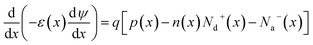
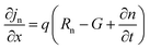
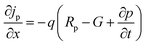
This study delves into the efficiency of Pb-free Cs2AgBiBr6 halide perovskite solar cells (PSCs) using 1D solar cell capacitance simulator (SCAPS-1D) software. The investigation encompasses the employment of graphene oxide (GO) as an ETL and copper oxide (Cu2O) as an HTL, with gold (Au) serving as the back contact metal. The hetero-structure design of FTO/GO/Cs2AgBiBr6/Cu2O/Au for the device, band diagram, grading of energy parameters, and J–V plot is demonstrated in Fig. 1(a–d). Moreover, the ultimate model incorporates an absorber layer with a thickness of 1500 nm and a defect density of 3.678 × 1016 cm−3. Additionally, doping levels for HTL and ETL are established at 9 × 10¹⁵ and 1 × 1015 cm−3. As illustrated in Fig. 1, it showcases distinctive characteristics of perovskite solar cells, specifically depicting the final J–V plot. Notably, open circuit voltage (Voc) is measured as 1.25 V, while short circuit current density (Jsc) is reached at 7.69 mA cm−2. Furthermore, the value of the Fill Factor (FF) is recorded as 41.31%, leading to the power conversion efficiency (PCE) of 3.99% as cited in Table 1.24 Additionally, an exploration into the influence of ETL and HTL layers performance, with absorber, HTL, and ETL thickness, series resistance, operational temperature, and quantum efficiency (QE) response was conducted.
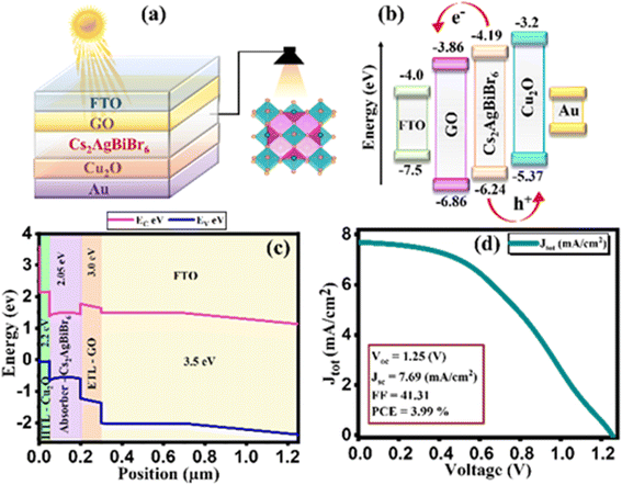 |
| | Fig. 1 (a) Device configuration of simulated perovskite solar cell, (b) energy-band diagram without contact between layers (c) energy-band diagram after contacts between layers (d) current density–voltage curve. | |
Table 1 Our simulation results of current density–voltage curves, for FTO/GO/Cs2AgBiBr6/Cu2O/Au cell
| FTO/GO/Cs2AgBiBr6/Cu2O |
| VOC (V) |
JSC (mA cm−2) |
FF (%) |
PCE (%) |
| 1.25 |
7.69 |
41.31 |
3.99 |
2. Simulation methodology
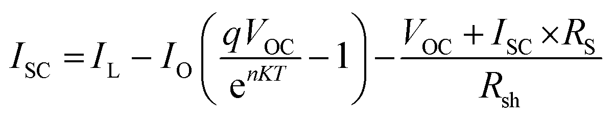
The simulation of solar cells using Solar Cell Capacitance Simulator (SCAPS 1-D) required various input parameters including the thickness of involving layers, bandgap, dielectric constant, electron affinity, carrier density, temperature, etc., and all these parameters are enlisted in Table 2. These input parameters have a direct influence on simulation outcomes. Key factors like material parameters, device geometry, and operational conditions directly impact the accuracy and relevance of simulated results such as carrier transport, recombination rates, and electrical characteristics. The sequence and summary of the simulation method are presented in Fig. 2. This software was developed at the Department of Electronics and Information Systems at the University of Gent, Belgium.25 This software is written in C programming language and allows for the calculation of various device architecture parameters, including grading, generation and recombination rates, and defects. Previous studies have already utilized SCAPS 1-D for simulating PSCs.26 This software employs numerical methods to solve Poisson's and continuity equations, enabling the calculation of parameters such as open-circuit voltage (VOC), photogenerated current density (JSC), fill factor (FF), and PCE.27,28 Below are the expressions for Poisson's equation (eqn (1)), electron continuity equation (eqn (2)) and hole continuity equation (eqn (3)):29| |
 | (1) |
| |
 | (2) |
| |
 | (3) |
Here, ε represents permittivity, q signifies the charge of an electron, ψ symbolizes electrostatic potential, n denotes overall electron density, p stands for total hole density, Nd+ represents the concentration of ionized donor as doping, Na− indicates the concentration of ionized acceptor as doping. Additionally, jn and jp are utilized to denote electron and hole current densities, while Rn and Rp correspond to net recombination rates for electrons and holes/unit volume, respectively. Finally, G represents generation rate/unit volume.
Table 2 Physical parameters of the PSC used in the simulation study
| Parameters |
Cu2O (HTL) |
Cs2AgBiBr6 |
GO (ETL) |
FTO |
| Thickness (nm) |
100 |
150 |
100 |
400 |
| Bandgap (eV) |
2.17 |
2.05 |
3.0 |
3.5 |
| Electron affinity (eV) |
3.2 |
4.19 |
3.86 |
4.0 |
| Dielectric permittivity |
7.1 |
5.8 |
9.0 |
9.0 |
| CB effective density of state (cm−3) |
2.5 × 10¹⁸ |
1.000 × 10¹⁶ |
2.2 × 10¹⁸ |
2.2 × 10¹⁷ |
| VB effective density of state (cm−3) |
2.5 × 10¹⁸ |
1.000 × 10¹⁶ |
1.8 × 10¹⁹ |
1.8 × 10¹⁷ |
| Electron thermal velocity (cm s−1) |
1.000 × 10⁷ |
1.000 × 10⁷ |
1.000 × 10⁷ |
1.000 × 10⁷ |
| Electron thermal velocity (cm s−1) |
1.000 × 10⁷ |
1.000 × 10⁷ |
1.000 × 10⁷ |
1.000 × 10⁷ |
| Electron mobility (cm2 V−1 s−1) |
2.0 × 10² |
11.81 |
1.0 × 10² |
2.0 × 101 |
| Hole mobility (cm2 V−1 s−1) |
8.0 × 10² |
0.49 |
3.0 × 101 |
1.0 × 101 |
| Shallow uniform donor density ND (cm−3) |
0 |
1.000 × 10¹⁹ |
1 × 10¹⁵ |
2.0 × 10¹⁷ |
| Shallow uniform acceptor density NA (cm−3) |
9.0 × 10¹⁵ |
1.000 × 10¹⁹ |
0 |
0 |
| Total density (Nt) |
1.0 × 10¹⁴ |
3.678 × 10¹⁶ |
1.0 × 10¹⁴ |
1.0 × 10¹⁵ |
| Ref. |
30 |
31 |
30 |
30 |
 |
| | Fig. 2 SCAPS simulation procedure. | |
3. Results and discussion
3.1. Effect of thickness of hole and electron transport layer
During this simulation, we tuned the thickness of the hole and electron transport layer to optimize the performance of solar cells.32 The optimization of transport layer thickness stands as a crucial endeavor in enhancing the efficiency of PSCs. In this pursuit, we finely tuned the thickness of the hole transport layer in the range of 0–200 nm and plotted the current density versus voltage graph at different thicknesses as depicted in Fig. 3(a). Furthermore, the values of JSC, and PCE exhibit discernible increments in response to varying hole transport layer thicknesses as tabulated in Table 3. This suggests that a thicker HTL enhances charge transport and collection within the device, leading to higher current generation and overall device performance. However, there is a decrease in open-circuit voltage (VOC) and fill factor (FF) as the HTL thickness increases, which could be attributed to increased series resistance and recombination losses within the device.33
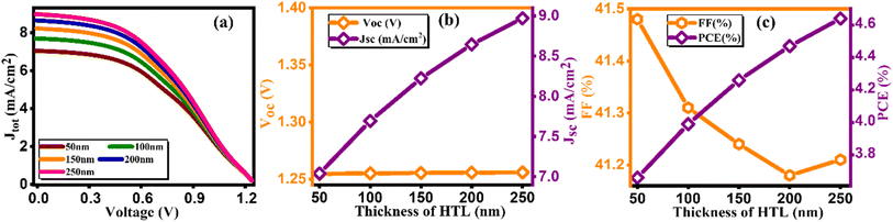 |
| | Fig. 3 Variation of (a) current density versus voltage, (b) Voc and Jsc, and (c) FF and PCE with thicknesses of HTL. | |
Table 3 Variation of performance indicators with thickness of HTL
| Thickness (nm) |
VOC (V) |
JSC (mA cm−2) |
FF (%) |
PCE (%) |
| 0 |
1.35 |
6.24 |
41.71 |
3.54 |
| 50 |
1.25 |
7.04 |
41.48 |
3.66 |
| 100 |
1.25 |
7.69 |
41.31 |
3.99 |
| 150 |
1.25 |
8.22 |
41.24 |
4.26 |
| 200 |
1.25 |
8.64 |
41.18 |
4.47 |
Notably, the paramount parameter, power conversion efficiency (PCE) (Fig. 3(c)), demonstrates a noteworthy increase, achieving a peak of 4.47% at an optimal thickness of 200 nm.34 Conversely, in tuning the thickness of the electron transport layer (ETL), the J–V curve along with other key factors are presented in Fig. 4(a–c) and computed key parameters, including VOC, JSC, FF, and PCE, are exhibited in Table 4. It is clearly seen that the increase in the thickness of the ETL leads to the degradation in the PV parameters for ETL, thereby leading to a decrement in PCE. This is due to the inefficient transport of charge carriers to the electrodes, the increase in series resistance that degrades the FF, and the increase in the probability of recombination with increasing ETL thickness. The same kind of behavior is reported by Hossain et al.35
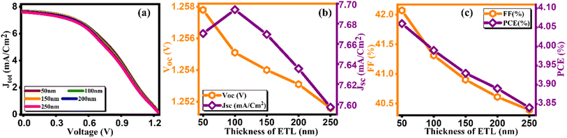 |
| | Fig. 4 Variation of (a) current density versus voltage, (b) Voc and Jsc, and (c) FF and PCE with thicknesses of ETL. | |
Table 4 Variation of performance indicators with thickness of ETL
| Thickness (nm) |
VOC (V) |
JSC (mA cm−2) |
FF (%) |
PCE (%) |
| 0 |
1.26 |
7.62 |
43.18 |
4.15 |
| 50 |
1.25 |
7.67 |
42.07 |
4.06 |
| 100 |
1.25 |
7.69 |
41.31 |
3.99 |
| 150 |
1.25 |
7.66 |
40.9 |
3.93 |
| 200 |
1.25 |
7.63 |
40.61 |
3.89 |
3.2. Effect of thickness of absorber layer
Perovskite, serving as an absorber layer, performs a pivotal part in dictating the overall performance of solar cells. Among various parameters influencing the device's functionality, the thickness of the absorber layer stands out as a critical factor.36 From Fig. 5(a) we observed the response of current density versus voltage plot of the absorber layer at different thicknesses. In our computational analysis, our primary focus revolves around evaluating key device performance metrics such as Jsc, VOC, FF, and PCE with varying absorber thicknesses, which span the range from 100 to 1000 nm as cited in Table 5.37 It's important to note that all other parameters remain constant. As visually represented in Fig. 5(b and c), outcomes of our simulations clearly demonstrate that an increase in absorber thickness leads to a noticeable rise in Jsc, peaking at approximately 9.57 mA cm−2 around the 500 nm thickness mark before experiencing a slight decline. In the context of a thin perovskite absorber, the charge carrier's diffusion length surpasses the thickness of the absorber, enabling the majority of excess carriers to efficiently reach their respective electrodes, thereby generating electrical power. The increment in thickness subsequently results in enhanced light absorption and an increased concentration of excess carriers, which in turn elevates Jsc values.38 This phenomenon is primarily attributed to the remarkably high absorption coefficient inherent in perovskite materials, which can often reach up to 105 cm−1. Consequently, thin absorber configurations tend to yield considerably high Jsc and PCE values, as demonstrated in Fig. 5(b and c). The behavior of Voc follows a distinct pattern, attaining an optimal value of 1.27 V at 100 nm thickness, after which it exhibits a steep decline, as depicted in Fig. 5(b). Voc is defined by equation given as:| |
 | (4) |
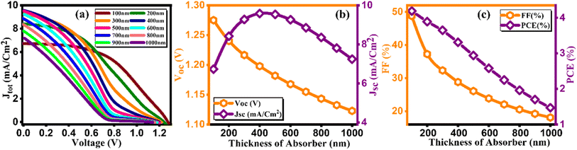 |
| | Fig. 5 Variation of (a) current density versus voltage, (b) Voc and Jsc, and (c) FF and PCE with thicknesses of Cs2AgBiBr6. | |
Table 5 Variation of performance indicators with thickness of absorber
| Thickness (nm) |
VOC (V) |
JSC (mA cm−2) |
FF (%) |
PCE (%) |
| 100 |
1.27 |
6.72 |
48.77 |
4.19 |
| 200 |
1.24 |
8.41 |
37.27 |
3.89 |
| 300 |
1.21 |
9.27 |
32.33 |
3.65 |
| 400 |
1.19 |
9.57 |
28.82 |
3.31 |
| 500 |
1.18 |
9.53 |
26.09 |
2.94 |
| 600 |
1.16 |
9.26 |
23.88 |
2.58 |
| 700 |
1.15 |
8.85 |
22.06 |
2.25 |
| 800 |
1.14 |
8.35 |
20.53 |
1.96 |
| 900 |
1.13 |
7.80 |
19.23 |
1.7 |
| 1000 |
1.12 |
7.24 |
18.11 |
1.47 |
In the above equation, n represents the ideality factor, KT/q signifies the thermal voltage, IL stands for the current generated by light, and IO denotes the current under dark saturation conditions. During the stage of increasing Voc, the recombination of holes and electrons is reduced in thinner absorber layers, maintaining a consistently low level.39 This leads to a higher concentration of excess carriers, which in turn facilitates the generation of a large Voc and promotes its emergence. However, in the stage of decreasing Voc, thicker absorber layers elevate to a higher level and provide more opportunities for carrier recombination, consequently leading to a pronounced drop in Voc. The Fill Factor (FF), as presented in Fig. 5(c), constantly reduces from 48.77 to 18.11 as the thickness of the absorber varies from 100–1000 nm. The FF is a measure of a solar cell's ability to efficiently deliver the generated power to an external load, representing internal power losses. In thicker absorbers, internal power losses intensify, resulting in a reduction of the FF. Fig. 5(c) provides further insights into the performance, particularly power conversion efficiency (PCE), which reaches its peak (4.19%) at 100 nm thickness but exhibits rapid decline with increasing thickness. Our simulations reveal that the efficiency of single junction perovskite solar cells (SJPSCs) is primarily governed by two aspects: carrier transport and photon absorption. Carrier transport becomes the dominant factor in thicker absorber layers, while photon absorption takes precedence in thinner absorber configurations. Consequently, it becomes evident that an optimal absorber thickness, typically ranging from 100 to 400 nm, corresponds to the highest achievable PCE. Beyond this optimal range, excessive absorber thickness leads to an increased presence of excess carriers and traps, creating a higher likelihood of recombination events, thus diminishing overall efficiency.
3.3. Effect of electron affinity for hole and electron transport layer
At the initial level of simulation, we want to probe the most suitable electron affinity value for HTL through the simulation process. Subsequently, this optimized value was incorporated into physical parameters listed in SCAPS-1D to facilitate additional simulations. The electron affinity is intricately connected with the lowest unoccupied molecular orbital (LUMO) of HTL and ETL and can be described as the energy required (in eV) to elevate free electron from the lowest point of LUMO (or conduction band in case of typical semiconductors) to the vacuum level. Aligning electron affinity with the appropriate energy band gap is crucial for enhancing the performance of the highest occupied molecular orbital (HOMO).40 This contributes to improved functioning of the electron/hole injection and blocking processes among perovskite material and HTL/ETL. However, it's essential to establish a practical numerical range for electron affinity values based on reported data for HTL before commencing simulation. This precaution is vital to avoid obtaining unrealistic physical parameters as outputs from the simulation results. Tables 6 and 7 present pertinent electronic parameters, including electron affinity, for the most commonly reported HTL and ETL, respectively. Fig. 6(a) and Fig. 7(a) demonstrate current density versus voltage plots for several electron affinity of HTL and ETL, respectively. From our analysis of the data, it's apparent that higher electron affinity is 4 eV for the electron/hole transport layer.41 Consequently, the feasible range of electron affinity values for our simulation falls within the bracket of 1.5 to 4.0 eV for HTL and 4 to 4.08 eV for ETL. We proceeded to calculate photovoltaic parameters by systematically varying the electron affinity values. Our objective was to identify the optimum electron affinity for the HTL and ETL in the context of Cs2AgBiBr6 based solar cell. The outcomes for HTL and ETL, including Voc, Jsc, FF, and PCE, are presented in Fig. 6(b, c), 7(b and c), respectively. These figures illustrate that the photovoltaic parameters, particularly Voc, Jsc, and FF, reach their maximum values, resulting in peak PCE of approximately 9.12% for HTL and 3.92% for ETL when electron affinity of HTL and ETL is set at 4.0 eV. Notably, the figure reveals that enhancing the electron affinity of HTL leads to improvements in Voc, Jsc, FF, and PCE. From Fig. 6(c), the increase in PCE correlates with increased electron affinity of HTL, optimizing electron extraction and minimizing charge recombination at the HTL/active layer interface in solar cells. Enhanced electron affinity aligns energy levels, improving charge transport efficiency and reducing energy losses, resulting in higher observed PCE values. Conversely, the rising electron affinity of ETL is linked to declining PCE due to unfavorable charge transport or increased recombination at the ETL/active layer interface, diminishing overall solar cell efficiency. This investigation unveils the effective role of electron affinity of HTL and ETL in optimizing the overall performance of solar cells.42
Table 6 Variation of performance indicators with electron affinity of HTL
| E.A of HTL (eV) |
VOC (V) |
JSC (mA cm−2) |
FF (%) |
PCE (%) |
| 1.5 |
0.16 |
0.01 |
21.89 |
0 |
| 2 |
0.46 |
0.77 |
10.76 |
0.04 |
| 2.5 |
0.57 |
5.69 |
24.82 |
0.81 |
| 3 |
1.05 |
7.58 |
36.53 |
2.92 |
| 3.5 |
1.56 |
7.76 |
47.82 |
5.82 |
| 4 |
2.14 |
7.81 |
54.41 |
9.12 |
Table 7 Variation of performance indicators with electron affinity of ETL
| E.A of ETL (eV) |
VOC (V) |
JSC (mA cm−2) |
FF (%) |
PCE (%) |
| 4 |
1.25 |
7.76 |
40.3 |
3.92 |
| 4.02 |
1.25 |
7.77 |
40.17 |
3.9 |
| 4.04 |
1.25 |
7.78 |
40.07 |
3.89 |
| 4.06 |
1.24 |
7.79 |
40.02 |
3.88 |
| 4.08 |
1.24 |
7.79 |
40.02 |
3.88 |
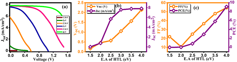 |
| | Fig. 6 Variation of (a) current density versus voltage, (b) Voc and Jsc, and (c) FF and PCE with electron affinity of HTL. | |
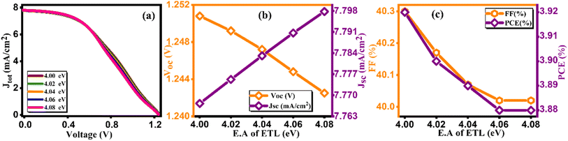 |
| | Fig. 7 Variation of (a) current density versus voltage, (b) Voc and Jsc, and (c) FF and PCE with electron affinity of ETL. | |
3.4. Effect of electron affinity of absorber layer
Initially, we maintained a constant value of electron affinity for both HTL and ETL, while systematically adjusting the electron affinity of the absorber layer, ranging from 3.0 to 4.0, as depicted in Fig. 8(a–c). Moreover, we plot the current density graph against voltage for different electron affinity of the absorber layer ranging from 3.0–4.0 eV, as illustrated in Fig. 8(a).43 The noticeable trend from Fig. 8(b and c) indicates a positive correlation between all four parameters (VOC, JSC, FF, and PCE) and a rise in electron affinity as listed in Table 8. As we observed from Fig. 8(c) there is an increase and then subsequent decrease in power conversion efficiency (PCE) with varying electron affinity of the absorber material suggesting an optimal range where charge extraction and carrier transport are most efficient, resulting in higher PCE. Deviations from this optimal range may lead to increased charge recombination or reduced charge extraction, thereby lowering overall efficiency. Remarkably, the simulated device achieved its highest PCE, reaching 7.19%, when electron affinity was set at 3.6 eV, marking a significant milestone in our investigation.44
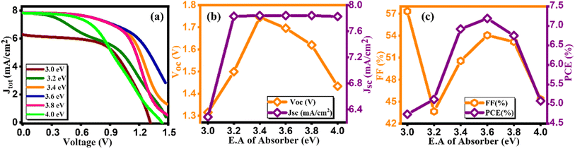 |
| | Fig. 8 Variation of (a) current density versus voltage, (b) Voc and Jsc, and (c) FF and PCE with electron affinity of Cs2AgBiBr6. | |
Table 8 Variation of performance indicators with electron affinity of absorber
| Electron affinity of absorber (eV) |
VOC (V) |
JSC (mA cm−2) |
FF (%) |
PCE (%) |
| 3 |
1.31 |
6.28 |
57.32 |
4.74 |
| 3.2 |
1.49 |
7.82 |
43.66 |
5.12 |
| 3.4 |
1.74 |
7.84 |
50.55 |
6.92 |
| 3.6 |
1.69 |
7.84 |
54.05 |
7.19 |
| 3.8 |
1.61 |
7.84 |
53.16 |
6.75 |
| 4 |
1.43 |
7.82 |
45.31 |
5.08 |
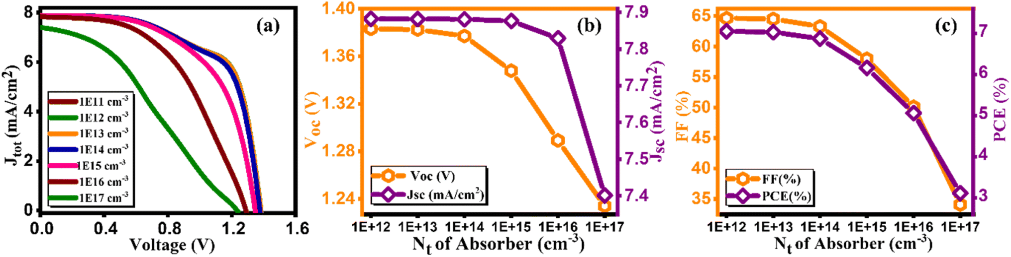
3.5. Effect of defect densities (Nt) of absorber layer
The defect density of the absorber layer is one of the crucial parameters that significantly control the efficiency of solar cells. In Cs2AgBiBr6, encompassing, point defects, interstitial, anti-site, and vacancy types, dominate the defect density landscape, although specific quantification of each type is not provided.45 The effectiveness of double perovskite solar cells is notably influenced by the quality and morphology of the perovskite layer. Suboptimal layer characteristic leads to an increase in defect density, resulting in an amplified recombination rate within the absorbing layer, consequently impeding solar cell performance. Fig. 9(a) illustrates the current density versus voltage graph for diverse defect densities (Nt) of Cs2AgBiBr6, spanning from 1011–1017 cm−3. Fig. 9(b and c) showcases how the Voc, Jsc, FF, and PCE vary in response to defect density (Nt), and their calculated values are mentioned in Table 9.46 As depicted in Fig. 9(c), device efficiency initiates at 7.05% at 1011, and 1012 cm−3, gradually decreasing to 7.03% at 1013, 6.87% at 1014, 6.16% at 1015, 5.06% at 1016, and 3.11% at 1017 cm−3. The Voc, Jsc, and FF values are also plotted in Fig. 9(b and c). The optimized values for these parameters are Voc of 1.38 V, Jsc of 7.88 mA cm−2, FF of 64.66%, and an efficiency of 7.05% achieved at a defect density of 1014 cm−3. The reduction in PV parameters with increasing defect density is attributed to the impact of defects on charge carrier recombination and transport. At lower defect densities, the device efficiency is relatively high due to fewer defects hindering charge movement. As the defect density increases, more defects act as non-radiative recombination centers, reducing the open-circuit voltage (Voc), short-circuit current density (Jsc), and fill factor (FF), ultimately leading to decreased device efficiency.
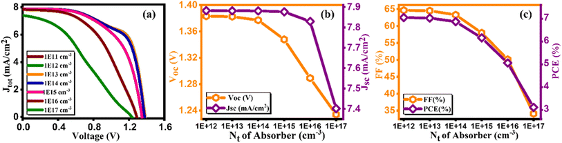 |
| | Fig. 9 Variation of (a) current density versus voltage, (b) Voc and Jsc, and (c) FF and PCE with defect density (Nt) of Cs2AgBiBr6. | |
Table 9 Variation of performance indicators with defect density of absorber
| Defect density of absorber (cm−3) |
VOC (V) |
JSC (mA cm−2) |
FF (%) |
PCE (%) |
| 1 × 10¹¹ |
1.38 |
7.88 |
64.66 |
7.05 |
| 1 × 10¹² |
1.38 |
7.88 |
64.65 |
7.05 |
| 1 × 10¹³ |
1.38 |
7.88 |
64.51 |
7.03 |
| 1 × 10¹⁴ |
1.37 |
7.88 |
63.29 |
6.87 |
| 1 × 10¹⁵ |
1.34 |
7.87 |
57.98 |
6.16 |
| 1 × 10¹⁶ |
1.28 |
7.82 |
50.12 |
5.06 |
| 1 × 10¹⁷ |
1.23 |
7.40 |
34.08 |
3.11 |
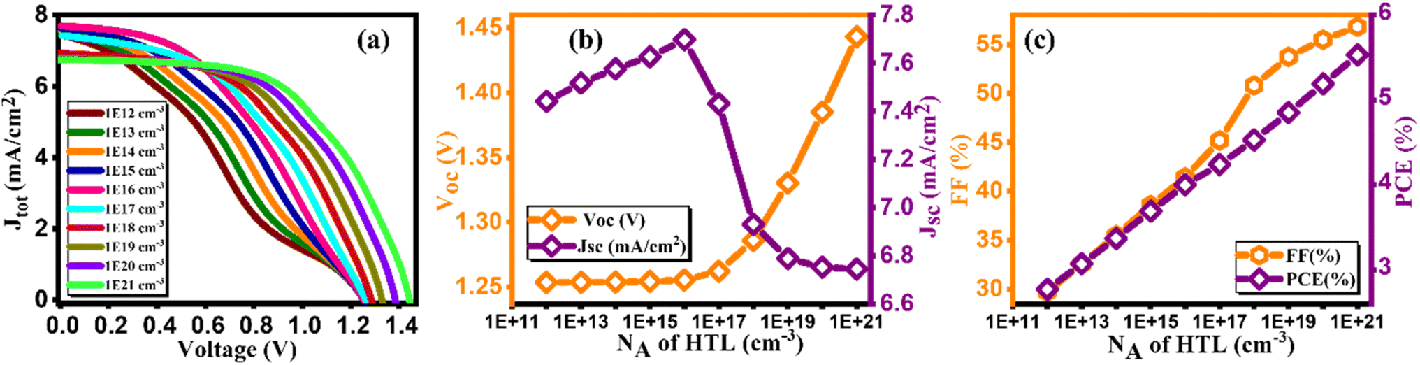
3.6. Effect of doping concentration (NA) of absorber layer
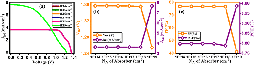
Fig. 10(a) provides a visual representation of current density versus voltage characteristics for varying the doping concentration in Cs2AgBiBr6, spanning from 1014 to 1019 cm−3. Intending to investigate the impact of varying doping concentrations of Cs2AgBiBr6 on device efficiency, we conducted a simulation study within the range of 1014 to 1019 cm−3.47 Observations from Fig. 10(b and c) reveal an initial increase in JSC, FF, and overall performance up to a particular threshold. However, further increments in doping content result in a decline in the output of a device, accompanied by a reduction in VOC from 1.35 to 1.25 V. The device achieved its highest PCE of 3.99% at 1019 cm−3 as tabulated in Table 10. Notably, there exists a correlation between doping concentration and electric field; as doping content rises, the electric field strength also rises. This upsurge in the electric field promotes rapid charge carrier separation, consequently enhancing device efficiency. In its optimized state, the device exhibited a VOC of 1.25 V, JSC of 7.69 mA cm−2, FF of 41.31%, and PCE of 3.99%.48
 |
| | Fig. 10 Variation of (a) current density versus voltage, (b) Voc and Jsc, and (c) FF and PCE with doping concentration (NA) of Cs2AgBiBr6. | |
Table 10 Variation of performance indicators with doping concentration of absorber
| Doping concentration NA of absorber |
VOC (V) |
JSC (mA cm−2) |
FF (%) |
PCE (%) |
| 1 × 10¹⁴ |
1.35 |
3.64 |
76.84 |
3.80 |
| 1 × 10¹⁵ |
1.35 |
3.64 |
76.84 |
3.80 |
| 1 × 10¹⁶ |
1.35 |
3.64 |
76.83 |
3.80 |
| 1 × 10¹⁷ |
1.36 |
3.64 |
76.82 |
3.80 |
| 1 × 10¹⁸ |
1.36 |
3.64 |
76.7 |
3.79 |
| 1 × 10¹⁹ |
1.25 |
7.69 |
41.31 |
3.99 |
3.7. Effect of doping concentration (NA) of HTL
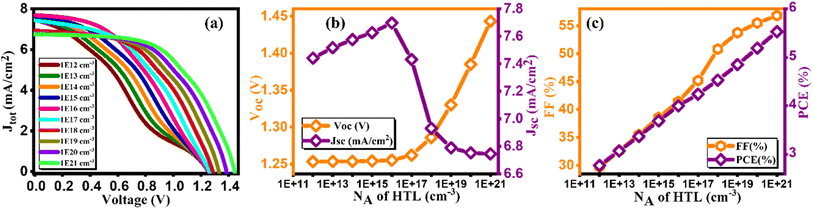
Fig. 11(a) illustrates the current density/voltage characteristics for a range of Cu2O doping contents, varying from 1012 to 1021 cm−3. The figure indicates that higher concentrations result in improved efficiency, attributed to enhanced extraction and charge transport at the Cu2O/absorber interface. In Fig. 11(b and c), the impact of acceptor doping concentration (NA) on performance parameters is depicted.49 It is observed that PCE is lower at lower NA levels, primarily due to elevated series resistance, aligning with prior research findings. Consequently, as demonstrated in Fig. 11(c), PCE is maximized at 1021 cm−3. This configuration yields Voc of 1.44 V, Jsc of 6.74 mA cm−2, FF of 56.8%, and an impressive efficiency of 5.53% as listed in Table 11.50
 |
| | Fig. 11 Variation of (a) Current density versus voltage, (b) Voc and Jsc, and (c) FF and PCE with doping concentration (NA) of HTL. | |
Table 11 Variation of performance indicators with doping concentration of HTL
| Doping concentration NA of HTL |
VOC (V) |
JSC (mA cm−2) |
FF (%) |
PCE (%) |
| 1 × 10¹² |
1.25 |
7.44 |
29.72 |
2.77 |
| 1 × 10¹³ |
1.25 |
7.51 |
32.56 |
3.07 |
| 1 × 10¹⁴ |
1.25 |
7.57 |
35.49 |
3.37 |
| 1 × 10¹⁵ |
1.25 |
7.62 |
38.56 |
3.69 |
| 1 × 10¹⁶ |
1.25 |
7.69 |
41.41 |
4.00 |
| 1 × 10¹⁷ |
1.26 |
7.43 |
45.18 |
4.24 |
| 1 × 10¹⁸ |
1.28 |
6.93 |
50.8 |
4.53 |
| 1 × 10¹⁹ |
1.33 |
6.78 |
53.73 |
4.85 |
| 1 × 10²⁰ |
1.38 |
6.75 |
55.47 |
5.19 |
| 1 × 10²¹ |
1.44 |
6.74 |
56.8 |
5.53 |
3.8. Effect of doping concentration (ND) of ETL
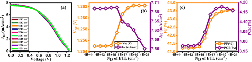
Fig. 12(a) exhibits a current density versus voltage graph for varying doping contents of GO, ranging from 1012 to 1021 cm−3. It is evident from this figure that higher concentrations result in enhanced extraction and charge transport at the GO/absorber interface. In Fig. 12(b and c), the impact of donor doping concentration (ND) on performance parameters is depicted. Once again, it is evident that PCE is adversely affected at lower ND levels, primarily due to increased series resistance, which aligns with the findings of previous studies.51 Consequently, as illustrated in Fig. 12(c), PCE reaches its maximum value of 4.18% at 1019 cm−3. This configuration yields Voc of 1.26 V, Jsc of 7.56 mA cm−2, and FF of 43.57% as mentioned in Table 12, representing notable achievement in solar cell efficiency.52
 |
| | Fig. 12 Variation of (a) current density versus voltage, (b) Voc and Jsc, and (c) FF and PCE with doping concentration (ND) of ETL. | |
Table 12 Variation of performance indicators with doping concentration of ETL
| Doping concentration ND of ETL |
VOC (V) |
JSC (mA cm−2) |
FF (%) |
PCE (%) |
| 1 × 10¹² |
1.25 |
7.69 |
41.23 |
3.98 |
| 1 × 10¹³ |
1.25 |
7.69 |
41.23 |
3.98 |
| 1 × 10¹⁴ |
1.25 |
7.69 |
41.23 |
3.98 |
| 1 × 10¹⁵ |
1.25 |
7.69 |
41.31 |
3.99 |
| 1 × 10¹⁶ |
1.25 |
7.69 |
41.84 |
4.05 |
| 1 × 10¹⁷ |
1.26 |
7.64 |
42.95 |
4.14 |
| 1 × 10¹⁸ |
1.26 |
7.63 |
43.32 |
4.17 |
| 1 × 10¹⁹ |
1.26 |
7.62 |
43.45 |
4.18 |
| 1 × 10²⁰ |
1.26 |
7.59 |
43.53 |
4.17 |
| 1 × 10²¹ |
1.26 |
7.56 |
43.57 |
4.16 |
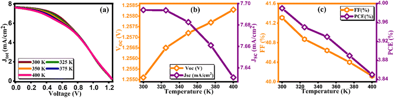
3.9. Effect of temperature on the cell performance
Perovskite solar cells (PSCs) offer simplicity in manufacturing and high light absorption efficiency, but their widespread adoption is hindered by stability issues. Factors like temperature, humidity, moisture, and ultraviolet radiation have notable impacts on PSC performance. Temperature, in particular, plays a critical role, as photovoltaic devices often operate under direct sunlight, which can lead to temperatures up to 45 °C higher than the ambient conditions.53 Temperature variations influence the semiconductor properties; lower temperatures narrow the semiconductor's bandgap, while higher temperatures increase the atom spacing and improve conductivity and electrical mobility. Fig. 13(a) illustrates the current density versus voltage plot. However, there is a noticeable correlation between elevated temperatures and increment in Voc as demonstrated in Fig. 13(b). This correlation can be attributed to the destabilization of electrons at high temperatures, increasing the likelihood of electron–hole recombination. The increased temperature also introduces more frequent scattering events, primarily lattice scattering, which hinders electron and hole movement. Consequently, carrier movement decreases due to scattering at higher temperatures, resulting in increased cell resistance. This effect is reflected in the decrease in fill factor (FF) from 41.31% to 40.12% in Fig. 13(c). Overall, the device's performance diminishes, leading to a reduction in PCE from 3.99% to 3.85% as cited in Table 13.54 This reduction in PCE with increasing temperature indicates thermal degradation of the solar cell components, leading to reduced performance due to increased carrier recombination and altered material properties at higher temperatures.
 |
| | Fig. 13 Variation of (a) current density versus voltage, (b) Voc and Jsc, and (c) FF and PCE with temperature. | |
Table 13 Variation of performance indicators with environmental temperature
| Temperature (K) |
VOC (V) |
JSC (mA cm−2) |
FF (%) |
PCE (%) |
| 300 |
1.25 |
7.69 |
41.31 |
3.99 |
| 325 |
1.25 |
7.69 |
40.87 |
3.95 |
| 350 |
1.25 |
7.68 |
40.64 |
3.93 |
| 375 |
1.25 |
7.66 |
40.4 |
3.89 |
| 400 |
1.25 |
7.63 |
40.12 |
3.85 |
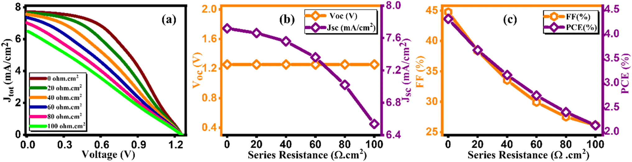
3.10. Effect of change in series resistance
In studies conducted under intense light, it has been established that the device's efficiency experiences a marginal improvement as a result of increasing light intensity. Nevertheless, it is imperative to note that the presence of series resistance (Rs) leads to certain inefficiencies within the PSC.55 Supplementary material illustrates the performance of the PSC device, wherein series resistance changes within the range of 0–100 Ω cm2 as depicted in Fig. 14(a–c). The current density versus voltage graph is plotted in Fig. 14(a). Notably, while series resistance exerts a limited influence on VOC, it exerts a substantial impact on both JSC and FF. This, in turn, culminates in a reduction of overall efficiency in perovskite solar cells. The interplay among VOC and JSC within PSCs might be effectively elucidated in the application of the diode equivalent circuit model, as mathematically expressed through the ensuing equations:56| |
 | (5) |
| |
 | (6) |
| |
 | (7) |
 |
| | Fig. 14 Variation of (a) current density versus voltage, (b) Voc and Jsc, and (c) FF and PCE with series resistance. | |
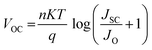
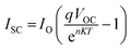
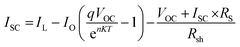
In this context, the term VOC pertains to voltage at an open circuit, while IL signifies current generated by incident light. Isc represents current at short circuit, and RS and Rsh denote resistances in series and shunt, respectively. JSC stands for current density, q signifies reverse saturation current, n represents ideality factor, K is Boltzmann constant, and T indicates temperature. Upon a close examination of the aforementioned equations, it becomes evident that an escalation in RS leads to a notable reduction in Isc, thereby directly impacting both FF and PCE. Within our current investigation, RS is subjected to variation within the range of 0 to 100 Ω cm2, which results in a decrease in the value of JSC (ranging from 7.72 to 6.54 mA cm−2) as illustrated in Fig. 14(b). This reduction in JSC, in turn, leads to a decline in FF (44.75%–26.15%) and device efficiency (4.33%–2.15%) as shown in Fig. 14(c) and cited in Table 14. It is noteworthy that VOC remains almost constant throughout this simulation. This constant value of VOC despite increasing series resistance suggests that series resistance does not significantly impact VOC in this scenario, indicating a possible dominance of other factors (such as shunt resistance or intrinsic material properties) in determining VOC in the solar cell. Furthermore, under ideal conditions, specifically at 0 Ω cm2, the simulated device showcased its highest attainable PCE, reaching 4.33%, as visually represented in Fig. 14(c). Overall, the decrease in PCE with increasing RS indicates that higher resistance leads to increased voltage losses and reduced current output, impacting overall efficiency by limiting charge transport and increasing energy dissipation within the solar cell.
Table 14 Variation of performance indicators with series resistance
| Series resistance (ohm cm2) |
VOC (V) |
JSC (mA cm−2) |
FF (%) |
PCE (%) |
| 0 |
1.25 |
7.71 |
44.75 |
4.33 |
| 20 |
1.25 |
7.66 |
38.36 |
3.69 |
| 40 |
1.25 |
7.55 |
33.53 |
3.18 |
| 60 |
1.25 |
7.36 |
29.91 |
2.76 |
| 80 |
1.25 |
7.02 |
27.49 |
2.42 |
| 100 |
1.25 |
6.53 |
26.15 |
2.15 |
3.11. QE characteristics
In Fig. 15, we observe the quantum efficiency (QE) variations with respect to the wavelength for double perovskite solar cell structure, both in the initial and final stages of optimization. The wavelength of incident light plays a crucial role in influencing QE.57 This parameter represents the ratio of charge carriers produced by solar cells to the incident photons striking semiconductor material. This relationship is well-documented in the literature.58 Additionally, it's worth noting that a thicker absorber tends to enhance photon absorption, resulting in an overall improvement in QE. This trend is supported by previous studies. Interestingly, our observations indicate that QE has the highest value at a wavelength of 350 nm, regardless of whether we consider the initial or final optimized conditions. However, beyond this range, there is a noticeable decrease in QE, confirming the intricate interplay between incident light wavelength and quantum efficiency. This finding holds true for both the initial and final optimization stages, as illustrated in Fig. 15.59
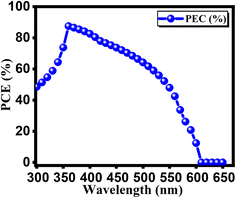 |
| | Fig. 15 Calculated quantum efficiency for FTO/GO/Cs2AgBiBr6/Cu2O. | |
3.12. Results of SCAPS-1D compared to previous research
In Table 15, we conduct a comprehensive comparison of photovoltaic performance parameters, taking into account recently published theoretical research work alongside our study. The data presented in the table unequivocally demonstrates that our work has achieved a notably higher Power Conversion Efficiency (PCE) in comparison to previously reported device configurations utilizing Cs2AgBiBr6.
Table 15 Comparison of PV parameters of Cs2AgBiBr6-based solar cells with the present study
| Device structure |
VOC (V) |
JSC (mA cm−2) |
FF (%) |
PCE (%) |
Ref. |
| ITO/SnO2/Cs2AgBiBr6/P3HT/Au |
1.09 |
1.73 |
0.76 |
1.44 |
60 |
| ITO/SnO2/Cs2AgBiBr6/Cu2O/Au |
1.17 |
3.42 |
0.78 |
3.13 |
60 |
| FTO/cTiO2/mTiO2/Cs2AgBiBr6/N719/spiro-OMeTAD/Ag |
1.06 |
5.13 |
— |
2.84 |
61 |
| FTO/TiO2/Cs2AgBiBr6/Sipro-OMeTAD/Au |
0.98 |
3.96 |
62.4 |
2.43 |
62 |
| FTO/GO/Cs2AgBiBr6/Cu2O |
2.14 |
7.81 |
54.41 |
9.12 |
Our work |
4. Conclusion
In our research, we conducted an extensive simulation using the SCAPS software, focusing on the exploration of inorganic, Pb-free Cs2AgBiBr6 perovskites for potential photovoltaic device applications. Our study examined various parameters, including the thickness of the electron transport layer (ETL), hole transport layer (HTL), and absorber, as well as defect density, doping concentration, electron affinity, temperature, and series resistance. Notably, the optimized results, for the Cs2AgBiBr6 perovskite device, underscored significant impacts stemming from variations in series resistance and temperature. Furthermore, the present study demonstrates a significant improvement in the PEC (9.12%) compared to the previously reported PEC values of 1.44, 3.13, 2.84, and 2.43% of double perovskite-based solar cells. Collectively, our findings offer not only encouragement but also valuable insights, paving the way toward the realization of inorganic and nontoxic perovskite solar cell devices. This research represents a substantial advancement in addressing environmental concerns associated with perovskite technology.
Data availability
All data included in this work can be provided on reasonable request.
Author contributions
Ghulam M. Mustafa: conceptualization, writing original draft, Bisma Younas: software, writing original draft, investigation, Sadaf Saba: writing original draft, methodology, software, Zainab Mufarreh Elqahtani: investigation; funding acquisition; software; resources, Norah Alwadai: project administration; formal analysis; writing – review & editing, Sikandar Aftab: resources and supervision
Conflicts of interest
There are no conflicts to declare.
Acknowledgements
The authors express their gratitude to Princess Nourah bint Abdulrahman University Researchers Supporting Project number (PNURSP2024R124), Princess Nourah bint Abdulrahman University, Riyadh, Saudi Arabia.
References
- F. Izadi, A. Ghobadi, A. Gharaati, M. Minbashi and A. Hajjiah, Optik, 2021, 227, 166061 CrossRef CAS.
- H. Q. Pham, R. J. Holmes, E. S. Aydil and L. Gagliardi, Nanoscale, 2019, 11(23), 11173–11182 RSC.
- G. Schileo and G. Grancini, J. Mater. Chem. C, 2021, 9(1), 67–76 RSC.
- G. Longo, S. Mahesh, L. R. Buizza, A. D. Wright, A. J. Ramadan, M. Abdi-Jalebi and H. J. Snaith, ACS Energy Lett., 2020, 5(7), 2200–2207 CrossRef CAS.
- I. Alam and M. A. Ashraf, Energy Sources, Part A, 2020, 1–17 Search PubMed.
- A. K. Chee, IEEE Trans. Electron Devices, 2019, 66(11), 4883–4887 CAS.
- M. A. Islam, N. A. Jahan and M. M. Hossain, Int. J. Environ. Clim. Change, 2022, 1–10 Search PubMed.
- X. Yang, W. Wang, R. Ran, W. Zhou and Z. Shao, Energy Fuels, 2020, 34(9), 10513–10528 CrossRef CAS.
- W. Gao, C. Ran, J. Xi, B. Jiao, W. Zhang, M. Wu and Z. Wu, ChemPhysChem, 2018, 19(14), 1696–1700 CrossRef CAS PubMed.
- A. K. Chee, IEEE Trans. Device Mater. Reliab., 2016, 16(2), 138–148 Search PubMed.
- W. Ning, F. Wang, B. Wu, J. Lu, Z. Yan, X. Liu and F. Gao, Adv. Mater., 2018, 30(20), 1706246 CrossRef PubMed.
- A. K. Chee, R. F. Broom, C. J. Humphreys and E. G. Bosch, J. Appl. Phys., 2011, 109(1), 1–10 CrossRef.
- E. H. Jung, N. J. Jeon, E. Y. Park, C. S. Moon, T. J. Shin, T. Y. Yang and J. Seo, Nat., 2019, 567(7749), 511–515 CrossRef CAS PubMed.
- P. Zhou, T. Bu, S. Shi, L. Li, Y. Zhang, Z. Ku and F. Huang, J. Mater. Chem., 2018, 6(21), 5733–5737 RSC.
- T. Burwig, M. Guc, V. Izquierdo-Roca and P. Pistor, J. Mater. Chem., 2020, 124(17), 9249–9255 CAS.
- Y. Dang, G. Tong, W. Song, Z. Liu, L. Qiu, L. K. Ono and Y. Qi, J. Mater. Chem., 2020, 8(1), 276–284 CAS.
- K. Z. Du, W. Meng, X. Wang, Y. Yan and D. B. Mitzi, Angew. Chem., Int. Ed. Engl., 2017, 56(28), 8158–8162 CrossRef CAS PubMed.
- M. Ghasemi, L. Zhang, J. H. Yun, M. Hao, D. He, P. Chen and L. Wang, Adv. Funct. Mater., 2020, 30(42), 2002342 CrossRef CAS.
- A. Ahmed, K. Riaz, H. Mehmood, T. Tauqeer and Z. Ahmad, Opt. Mater., 2020, 105, 109897 CrossRef CAS.
- N. S. N. M. Alias, F. Arith, A. N. Mustafa, M. M. Ismail, N. F. Azmi and M. S. Saidon, J. Eng. Technol. Sci., 2022, 54(4), 220409 CrossRef.
- S. Rai, B. K. Pandey, A. Garg and D. K. Dwivedi, Opt. Mater., 2021, 121, 111645 CrossRef CAS.
- S. Das, M. G. Choudhury, S. Paul and J. Nano- Electron, Phys., 2022, 14(3), 03012 CAS.
- I. Alam, R. Mollick and M. A. Ashraf, Phys. Rev. B: Condens. Matter Mater. Phys., 2021, 618, 413187 CrossRef CAS.
- A. Slami, M. Bouchaour and L. Merad, Int. J. Energy Environ., 2019, 3, 17–21 Search PubMed.
- M. Burgelman, K. Decock, A. Niemegeers, J. Verschraegen, and S. Degrave, SCAPS Manual. University of Ghent, Ghent, Belgium, 2016 Search PubMed.
- M. A. Ashraf and I. Alam, Eng. Res. Express, 2020, 2(3), 035015 CrossRef.
- A. K. Kang, M. H. Zandi and N. E. Gorji, Opt. Quantum Electron., 2019, 51, 1–9 CrossRef CAS.
- M. Burgelman, P. Nollet and S. Degrave, Thin solid films, 2000, 361, 527–532 CrossRef.
- M. T. Islam, M. R. Jani, S. M. Al Amin, M. S. U. Sami, K. M. Shorowordi, M. I. Hossain and S. Ahmed, Opt. Mater., 2020, 105, 109957 CrossRef CAS.
- A. Chauhan, A. Oudhia and A. K. Shrivastav, J. Mater. Sci.: Mater. Electron., 2022, 33(3), 1670–1685 CrossRef CAS.
- A. Mohandes, M. Moradi and H. Nadgaran, Opt. Quantum Electron., 2021, 53, 1–22 CrossRef.
- D. P. Pham, S. Lee, Y. Kim and J. Yi, J. Phys. Chem. Solids, 2021, 154, 110059 CrossRef CAS.
- H. D. Um, S. A. Moiz, K. T. Park, J. Y. Jung, S. W. Jee, C. H. Ahn and J. H. Lee, Appl. Phys. Lett., 2011, 98(3), 153110 CrossRef.
- M. R. Jani, M. T. Islam, S. M. Al Amin, M. S. U. Sami, K. M. Shorowordi, M. I. Hossain and S. Ahmed, Superlattices Microstruct., 2020, 146, 106652 CrossRef CAS.
- M. K. Hossain, G. I. Toki, A. Kuddus, M. H. K. Rubel, M. M. Hossain, H. Bencherif and M. Mushtaq, Sci. Rep., 2023, 13(1), 2521 CrossRef CAS PubMed.
- K. Chakraborty, M. G. Choudhury and S. Paul, Sol. Energy, 2019, 194, 886–892 CrossRef CAS.
- T. Leijtens, J. Lim, J. Teuscher, T. Park and H. J. Snaith, Adv. Mater., 2013, 25(23), 3227–3233 CrossRef CAS PubMed.
- J. M. Frost, K. T. Butler, F. Brivio, C. H. Hendon, M. Van Schilfgaarde and A. Walsh, Nano Lett., 2014, 14(5), 2584–2590 CrossRef CAS PubMed.
- T. Minemoto, Y. Kawano, T. Nishimura and J. Chantana, Opt. Mater., 2019, 92, 60–66 CrossRef CAS.
- N. K. Noel, S. D. Stranks, A. Abate, C. Wehrenfennig, S. Guarnera, A. A. Haghighirad and H. J. Snaith, Energy Environ. Sci., 2014, 7(9), 3061–3068 RSC.
- N. Marinova, W. Tress, R. Humphry-Baker, M. I. Dar, V. Bojinov, S. M. Zakeeruddin and M. Grätzel, ACS Nano, 2015, 9(4), 4200–4209 CrossRef CAS PubMed.
- G. W. Kim, D. V. Shinde and T. Park, RSC Adv., 2015, 5(120), 99356–99360 RSC.
- L. Xiong, Y. Guo, J. Wen, H. Liu, G. Yang, P. Qin and G. Fang, Adv. Funct. Mater., 2018, 28(35), 1802757 CrossRef.
- A. Raj, M. Kumar, H. Bherwani, A. Gupta and A. Anshul, J. Vac. Sci. Technol., B: Nanotechnol. Microelectron.: Mater., Process., Meas., Phenom., 2021, 39(1), 030802 Search PubMed.
- H. Baig, H. Kanda, A. M. Asiri, M. K. Nazeeruddin and T. Mallick, Sustainable Energy Fuels, 2020, 4(2), 528–537 RSC.
- L. Zhu, D. Liu, J. Wang and N. Wang, J. Phys. Chem. Lett., 2020, 11(20), 8502–8510 CrossRef CAS PubMed.
- R. Teimouri, Z. Heydari, M. P. Ghaziani, M. Madani, H. Abdy, M. Kolahdouz and E. Asl-Soleimani, Superlattices Microstruct., 2020, 145, 106627 CrossRef CAS.
- M. Keshavarz, E. Debroye, M. Ottesen, C. Martin, H. Zhang, E. Fron and J. Hofkens, Adv. Mater., 2020, 32(40), 2001878 CrossRef CAS PubMed.
- F. Zhang and K. Zhu, Adv. Energy Mater., 2020, 10(13), 1902579 CrossRef CAS.
- A. Daraie and A. Fattah, Opt. Mater., 2020, 109, 110254 CrossRef CAS.
- B. Wang, J. Yang, L. Lu, W. Xiao, H. Wu, S. Xiong and Q. Bao, Adv. Mater. Interfaces, 2020, 7(6), 1901964 CrossRef CAS.
- S. Jamal, A. D. Khan and A. D. Khan, Optik, 2020, 218, 164787 CrossRef CAS.
- T. He, Y. Jiang, X. Xing and M. Yuan, Adv. Mater., 2020, 32(26), 1903937 CrossRef CAS PubMed.
- K. Sobayel, M. Akhtaruzzaman, K. S. Rahman, M. T. Ferdaous, Z. A. Al-Mutairi, H. F. Alharbi and N. Amin, Results Phys., 2019, 12, 1097–1103 CrossRef.
- H. I. Alkhammash, M. Mottakin, M. M. Hossen, M. Akhtaruzzaman and M. J. Rashid, Semicond. Sci. Technol., 2022, 38(1), 015005 CrossRef.
- T. Minemoto and M. Murata, Sol. Energy, 2015, 133, 8–14 CAS.
- N. Mundhaas, Z. J. Yu, K. A. Bush, H. P. Wang, J. Häusele, S. Kavadiya and Z. C. Holman, Sol. RRL, 2019, 3(4), 1800378 CrossRef.
- M. K. Hossain, M. H. K. Rubel, G. I. Toki, I. Alam, M. F. Rahman and H. Bencherif, ACS omega, 2022, 7(47), 43210–43230 CrossRef CAS PubMed.
- M. F. Rahman, M. J. A. Habib, M. H. Ali, M. H. K. Rubel, M. R. Islam, A. B. Md Ismail and M. K. Hossain, AIP Adv., 2022, 12(10), 105317 CrossRef CAS.
- A. Mohandes, M. Moradi and H. Nadgaran, Opt. Quantum Electron., 2021, 53, 1–22 CrossRef.
- X. Yang, Y. Chen, P. Liu, H. Xiang, W. Wang, R. Ran and Z. Shao, Adv. Funct. Mater., 2020, 30(23), 2001557 CrossRef CAS.
- M. S. Shadabroo, H. Abdizadeh and M. R. Golobostanfard, ACS Appl. Energy Mater., 2021, 4(7), 6797–6805 CrossRef CAS.
|
| This journal is © The Royal Society of Chemistry 2024 |
Click here to see how this site uses Cookies. View our privacy policy here. 
 Open Access Article
 This Open Access Article is licensed under a
  *a,
Bisma Younasb,
Sadaf Saba
*a,
Bisma Younasb,
Sadaf Saba