
 Open Access Article
 This Open Access Article is licensed under a Creative Commons Attribution-Non Commercial 3.0 Unported Licence
Ambient stable solution-processed organic field effect transistors from electron deficient planar aromatics: effect of end-groups on ambient stability†
Indrajit
Giri
 a,
Sagar
Biswas
a,
Shant
Chhetri
a,
Anwesha
Choudhuri
b,
Indrajit
Mondal
c,
Satyaprasad P.
Senanayak
c,
Parameswar Krishnan
Iyer
*b,
Debangshu
Chaudhuri
a and
Ratheesh K.
Vijayaraghavan
*a
a,
Sagar
Biswas
a,
Shant
Chhetri
a,
Anwesha
Choudhuri
b,
Indrajit
Mondal
c,
Satyaprasad P.
Senanayak
c,
Parameswar Krishnan
Iyer
*b,
Debangshu
Chaudhuri
a and
Ratheesh K.
Vijayaraghavan
*a
aDepartment of Chemical Sciences, Indian Institute of Science Education and Research Kolkata, Mohanpur, Nadia, West Bengal 741246, India
bCentre for Nanotechnology, Indian Institute of Technology, Guwahati, Assam 781039, India
cNanoelectronics and Device Physics Lab, School of Physical Sciences, National Institute of Science Education and Research, OCC of HBNI, Odisha 752050, India. E-mail: pki@iitg.ac.in; ratheesh@iiserkol.ac.in
First published on 6th March 2024
Abstract
Ambient stable solution processed n-channel organic field effect transistors (OFETs) are essential for next-generation low-cost organic electronic devices. Several molecular features, such as suitable orbital energy levels, easy synthetic steps, etc., must be considered while designing efficient active layer materials. Here, we report a case of improved ambient stability of solution-processed n-type OFETs upon suitable end-groups substitution of the active layer materials. A pair of core-substituted napthalenediimide (NDIFCN2 and EHNDICN2) derivatives with alkyl and perfluorinated end groups are considered. The transistor devices made out of these two derivatives exhibited largely different ambient stability behavior. The superior device stability (more than 25 days under ambient conditions) of one of the derivatives (NDIFCN2) was ascribed to the presence of fluorinated end groups that function as hydrophobic guard units inhibiting moisture infiltration into the active layer, thereby achieving ambient stability under humid conditions (>65% relative atmospheric humidity). Molecular level optical and electrochemical properties, thermal stability, and the solution-processed (spin coat and drop cast active layers) device characteristics are described in detail. Our findings highlight the requirement of hydrophobic end groups or sidechains for ambient stability of active layer materials, along with deep LUMO levels for ambient stability.
1. Introduction
The ongoing exploration of organic semiconductors (OSCs) for applications in organic electronic devices, such as field-effect transistors (OFETs), remains intriguing due to their convenient fabrication of films and devices from solution. These versatile devices find applications in various uses, from lightweight and flexible logic circuits.1,2 To meet these demands, maintaining well-balanced charge transport is essential. Although substantial strides have been made in enhancing the performance of high-quality p-type OSCs,3,4 there has been significantly less progress in n-type OSCs, particularly in the ambient stability of such devices. A primary requisite for low molecular weight organic n-type semiconductors to be ambient stable is the deep LUMO (Lowest Unoccupied Molecular Orbital) energy (<−4 eV), demonstrated for ambient stable OFETs.5–11 Far more low-lying LUMOs below −4.5 eV have adverse effects on the stability of molecules.12,13 An ideal LUMO energy level window is −4.0 to −4.5 eV. Furthermore, hydrophobic sidechains have also been known to improve the ambient stability of the active layer by safeguarding it against moisture infiltration during device fabrication and operation.14,15 Self-assembly of such molecular semiconductors in the bulk layer can give rise to good carrier mobility (µ) if sufficient intermolecular orbital overlap exists. Hence, weak van der Waals interactions across the molecular assembly can be crucial in driving suitable molecular orientation in the film state.16–18 In addition to the ambient stability of the devices, low-operational voltage is also essential to ensure commercial viability.19 Although benchmark p-type materials with ambient stability and high electrical performance are known in the literature,20–22 reports on electron-deficient n-type counterparts are limited. The intricate synthetic procedures required in developing these materials contribute to this. Achieving electron-deficient π-electron systems is challenging as they often incorporate electron-deficient atoms in the acene structures. Alternatively, substituting the electron-deficient groups directly into the backbone is also an effective strategy that is synthetically less challenging.Heeney et al. reported favourable ambient stability in solution-processed OFETs, utilizing an indacenodithiophene (IDT) core and different acceptor end groups like 2,1,3-benzothiadiazole-4,5,6-tricarbonitrile (TCNBT) and TFBT, exhibited a noteworthy retention of approximately 73% in saturation mobility throughout 100 hours of ambient stability measurements.23 The reported LUMO values are approximately −4 eV. In another report, they demonstrated that during ambient stability measurements of OFETs, the diFIDT–di(C(CN)2) OSC with a LUMO level of −4.24 eV experienced a reduction in mobility, decreasing by approximately half after 100 hours.24 In contrast, Bao et al. demonstrated that NDI and dechlorinated-NDI with –CH2C3F7/–CH2C4F9 side chains, featuring LUMO values ranging from −3.72 to −4.13 eV, exhibited a retention of mobility values between 39% and 65% throughout 45 days of ambient stability measurements.25 Würthner et al. also reported single crystal devices utilizing dechlorinated NDI with –CH2C3F7 side chains, revealing a degradation of less than 13% over three months under ambient conditions.26 These findings underscore the extra advantages of hydrophobic fluoroalkyl chains, regardless of their comparable LUMO energy levels, for achieving ambient stability, extending from 100 hours to over a month.
Here, we attempt to compile the strategy of lowering the LUMO by substituting with electron-withdrawing groups at the charge hoping centres (aromatic units) and hydrophobic end groups to molecular systems of napthalenediimide (NDI) based n-type materials for ambient stable electron channel devices. The –CN groups connected to C-4 and C-9 positions of the NDI core with symmetrically substituted heptafluorobutyl (NDIFCN2) and ethylhexyl (EHNDICN2) end groups are considered here to compare the effect of end groups. The chemical structure and the synthesis are summarized in Scheme 1. Substituting –CN groups at the NDI core are known to lower the LUMO energy. Density functional theory (DFT) calculations at the B3LYP/6-31+G(d) level indicated that the fluorinated end groups also assist in pushing the LUMO further deeper than the alkyl counterpart.27 For EHNDICN2, the calculated LUMO energy level was −4.18 eV, whereas NDIFCN2 was −4.53 eV (Fig. S8†). Molecular photophysical, electrochemical and charge transport features of the bulk materials in their OFETs are summarized in the article.
 | ||
| Scheme 1 The synthetic procedure of NDIFCN2 and EHNDICN2. | ||
2. Experimental section
2.1. Materials and methods
All chemicals were purchased from Sigma-Aldrich, Merck, Spectrochem Pvt. Ltd., and Alfa Aesar and used without further purification. All the solvents were purchased from Sigma-Aldrich, Merck and Spectrochem Pvt. Ltd. Solvents were purified, degassed with argon, and stored over activated molecular sieves (4 Å).2.2. Characterization and instrumentation
NMR analysis of EHNDICN2 and NDIFCN2 was carried out with JEOL 400 MHz and BRUKER 500 MHz NMR in CDCl3 at 25 °C. Coupling constants (J) are reported in Hertz (Hz). Coupling patterns are indicated as s (singlet), d (doublet), t (triplet), or m (multiplet). The elemental analyses were carried out with a PerkinElmer 240C elemental analyzer. DSC experiment was carried out at a scan rate of 5 °C min−1 TGA was performed at a heating rate of 10 °C min−1 with a sample weight of 2–3 mg in a nitrogen atmosphere. Unless otherwise mentioned, all other experiments were conducted at room temperature 25 ± 1 °C. XRD measurements were carried out with Rigaku X-ray diffractometer (Cu Kα irradiation, λ = 1.541 Å). AFM images were taken with NT-MDT NTEGRA instrument from NT-MDT (Santa Clara, CA). UV-vis absorption spectra were recorded using a Jasco V-670 spectrophotometer, and PL spectra were measured with a Horiba Fluoromax instrument. To capture the structure and relative orientation of the film, a higher X-ray energy (18 keV) was employed to cover a wide range of scattering angles using a large 2D PerkinElmer detector (2048 pixels by 2048 pixels) at the P08 beamline, PETRA III, DESY, Germany. A beam defining slits of 300 µm in vertical and 600 µm in horizontal direction were used. The incidence angle was varied between 0.1–0.3° to maximize the film signal during the grazing incidence X-ray scattering (GIXS) measurements.2.3. Solution-processed device fabrication
Heavily n-doped silicon (n++-Si) and 300 nm SiO2 layer were used as the gate electrode and dielectric insulator (capacitance Ci = 9 nF cm−2). It was cleaned by known protocols of three-stage detergent-water and solvents: 2% Hellmanex solution in water (ultrasonication for 30 minutes), stepwise sonication, and wash with fresh Milli-Q water for three times and subsequent rinse and wash with acetone, isopropanol, and UV-ozone exposure for 1 hour. The cleaned substrates were modified with n-OTS (trichloro(octyl)silane). In the active layer deposition, a solution of EHNDICN2 was prepared in chloroform (5 g L−1) at 45 °C and stirred and deposited on the cleaned OTS-treated substrates using a spin-coat process at a spinning rate of 2500 rpm for 40 s and NDIFCN2, a solution of 4–5 g L−1 in o-dichlorobenzene (o-DCB) at 120 °C and stirring and deposited at a spinning rate of 2500 rpm for 60 s at heating condition. The substrates were subjected to thermal annealing at 120 °C for 10 minutes and then transferred to a vacuum desiccator. For EHNDICN2 devices, n-OTS modified Si/SiO2 substrates, and for NDIFCN2, bare substrates were used. In the case of NDIFCN2, the films prepared on OTS-modified layers were highly inhomogeneous. This was attributed to a significant difference in the surface energy and wettability due to fluorinated end groups. Fig. S9† shows the photographs indicating the wettability of o-DCB solutions of both the molecules on the OTS-treated substrates. The difference in wettability is quite evident.
NDIFCN2 was dissolved in o-DCB at 0.5 g L−1 at 120 °C with stirring for drop cast films. 80 µL solution was drop-casted on top of hot (100 °C) 2 × 2 cm. Si/SiO2 substrate and kept covered with cover glass for 5 minutes. Substrates were then annealed at 120 °C for 10 minutes and transferred to a vacuum desiccator. After 12 h, Au as drain and source electrodes (thickness 180–200 nm) was vacuum deposited on top of the thin films at a deposition rate of 10 Å s−1 under a pressure of 10−6 mbar through a shadow mask, where the channel length (L) and width (W) were 60 µm and 1.6 cm, respectively. Current–voltage (I–V) characteristics of the devices were always measured under 10−5 mbar vacuum conditions with a Keithley 4200A-SCS semiconductor characterization system. Field-effect mobility was calculated in the saturation regime of Id using the following equation:

3. Results and discussion
3.1. Synthesis and characterization
Both the compounds were obtained by following three-step reactions viz, bromination of naphthalene dianhydride by 1,3-dibromo-5,5-dimethylhydantoin (DBH) in c. H2SO4, subsequently imide formation by alkyl-amine in acetic acid medium, and the CN group incorporation using CuCN in dimethylformamide (DMF). All the characterization data are summarized in ESI.† We observed good solubility (∼16 mg mL−1) for EHNDICN2 in common organic solvents like chloroform (CHL), ethylacetate and 1,2-dichlorobenzene (o-DCB). However, the solubility of NDIFCN2 in these solvents was found to be lesser (∼4–5 mg mL−1).![[thin space (1/6-em)]](https://www.rsc.org/images/entities/char_2009.gif) :hexane) to yield NDIFCN2 (66 mg, 48%). 1H NMR (400 MHz, CDCl3): δ = 9.15 (s, 2H), 5.02–5.09 (t, 4H). (ESI-MS): calcd for (M + Na) C24H6N4O4NaF14 was 703.006, found: 703.4. 13C NMR (500 MHz, acetone-D6) δ 160.8, 160.5, 135.7, 129.3, 128.2, 127.4, 124.5, 118.9, 116.3, 115.8, 115.1, 108.6, 39.07.
:hexane) to yield EHNDICN2 (190 mg, 35%). 1H NMR (400 MHz, CDCl3) δ = 9.03 (s, 2H), 4.24–4.10 (m, 4H), 1.99–1.91 (m, 1H), 1.46–1.14 (m, 16H), 0.90 (dt, J = 19.0, 7.0 Hz, 12H). 13C NMR (500 MHz, CDCl3) δ 160.46, 160.03, 136.07, 128.58, 127.53, 127.15, 116.90, 115.78, 45.51, 37.78, 30.58, 28.47, 23.95, 23.02, 14.03, 10.50.
:hexane) to yield NDIFCN2 (66 mg, 48%). 1H NMR (400 MHz, CDCl3): δ = 9.15 (s, 2H), 5.02–5.09 (t, 4H). (ESI-MS): calcd for (M + Na) C24H6N4O4NaF14 was 703.006, found: 703.4. 13C NMR (500 MHz, acetone-D6) δ 160.8, 160.5, 135.7, 129.3, 128.2, 127.4, 124.5, 118.9, 116.3, 115.8, 115.1, 108.6, 39.07.
:hexane) to yield EHNDICN2 (190 mg, 35%). 1H NMR (400 MHz, CDCl3) δ = 9.03 (s, 2H), 4.24–4.10 (m, 4H), 1.99–1.91 (m, 1H), 1.46–1.14 (m, 16H), 0.90 (dt, J = 19.0, 7.0 Hz, 12H). 13C NMR (500 MHz, CDCl3) δ 160.46, 160.03, 136.07, 128.58, 127.53, 127.15, 116.90, 115.78, 45.51, 37.78, 30.58, 28.47, 23.95, 23.02, 14.03, 10.50.
3.2. Optical and electrochemical properties
Optical absorption spectra of the monomeric solution state and film samples were compared to understand the interchromophoric interactions. Fig. 1a compares normalized absorption spectra of molecularly dissolved and aggregated thin films of EHNDICN2 (top panel) and NDIFCN2 (bottom panel). In CHCl3, both molecules exist in a molecularly dissolved state, as indicated by their structured absorption spectra and clearly defined vibronic peaks at 392 (±1), 378, 374 (±1) nm, and 358 (±1) nm. However, the thin-film absorption spectra of the two compounds exhibit noticeable differences. For EHNDICN2, the spectrum undergoes broadening, and the 0–0 peak shifts to 401 nm, while the relative intensities of various vibronic peaks remain nearly unchanged. However, for NDIFCN2, the alterations are considerably more pronounced. | ||
| Fig. 1 (a) Solution and film state absorption spectra, (b) Cyclic voltammograms in CH2Cl2 solvent (vs. Fc/Fc+), blue arrow-lines indicate first onset reduction potentials. (c) DSC, and (d) TGA analysis. Yellow traces represent the EHNDICN2, and the green traces that of NDIFCN2. | ||
The 0–0 peak shifts to 405 nm and exhibits a considerably higher oscillator strength than the other two vibronic peaks at 381 and 361 nm, consistent with a J-type excitonic coupling.30
Redox properties of NDIFCN2 and EHNDICN2 were studied by cyclic voltammetry (CV) in CH2Cl2 at 25 °C, using Au as working, Ag/AgCl as the reference, and Pt as the counter electrodes, respectively (please see the ESI† for experimental details).31 Two consecutive reversible reductions are evident from the (Fig. 1b) voltammogram for both molecules. The voltammogram revealed two electron-reversible reduction peaks (Fig. 1b), emphasizing the considerable electron affinity of these molecules with the observed reduction onset (Eonsetred). The first Eonsetred appear at 0.18 V & −0.01 V for NDIFCN2 & EHNDICN2 respectively. From the first reduction potentials, the LUMO energy levels are estimated (equation given in ESI†) to be −4.5 eV & −4.31 eV (Fc/Fc+ was used as the internal standard). The fully reversible reduction signals confirm the redox stability of these two molecules, which is essential to achieve active layer materials with bias stress stability. The low-lying LUMO levels of both molecules are expected to facilitate ambient stability to the active layer in the OFET devices.
3.3. Thermal properties
The thermal stability of NDIFCN2 and EHNDICN2 were examined by differential scanning calorimetry (DSC) and thermal gravimetric analysis (TGA), summarized in Fig. 1c and d, respectively. From the DSC thermogram, sharp endothermic crystal melting transitions were evident with the melting temperature (Tm) of NDIFCN2 at 414.4 °C, which was much higher in comparison to that of EHNDICN2 (Tm = 283.74 °C), which can be correlated to the fact that ethylhexyl end group is more extended in comparison to that of the fluorinated chain in NDIFCN2. The long, branched side chains are expected to provide more disordered solids in the case of EHNDICN2 and low melting point. A higher melting point of the fluorinated derivatives can be attributed to strong intermolecular CF–π interactions that reduce the solid-state disorder originating from the conformationally flexible side chains. From thermogravimetric analysis, both the compounds showed excellent thermal stability, and the onset of decomposition temperatures (Td: temperature where 10% weight loss reached) were found to be >350 °C. Nevertheless, these materials remain stable under the processing conditions (at 120 °C) and the device operating conditions (at 25 °C).3.4. OFET performances
OFET characteristics of NDIFCN2 and EHNDICN2 were studied using a bottom-gate top-contact (BG-TC) device configuration unless otherwise mentioned. Both solution-processed and vapour-deposited active layer materials were used for the devices. Thermally evaporated gold (Au) on the active layers served as the source and drain electrodes. Devices made from these two NDI derivatives exhibited clear output and transfer characteristics. Saturation field effect mobility was extracted from the transfer characteristics. Highly reproducible current traces were observed for these two derivatives. For the OFETs based on the solution-processed active layer, NDIFCN2 demonstrates saturation regime electron mobility (µmaxe) up to 4.0 × 10⁻³ cm2 V−1 s−1 with a very low threshold voltage (Vth = −1.25 V) and an on/off current ratio (Ion/Ioff) > 103, while for the EHNDICN2 devices, the µmaxe was 1.6 × 10⁻² cm2 V−1 s−1, Vth −2.0 V, and Ion/Ioff > 104. The µmaxe for the devices obtained from the thermally evaporated active layer was nearly an order larger in the case of NDIFCN2 (1.6 × 10⁻² cm2 V−1 s−1) and was more than double in the case of EHNDICN2 (4.0 × 10⁻² cm2 V−1 s−1) (Fig. S10†). The µmaxe and µavge was found to be less for NDIFCN2 (over 30 devices) in comparison to the other derivative despite the deposition and layer processing conditions. This was attributed to the least favoured aromatic ring overlap in the π stacking direction, as evident from the single crystal X-ray structure analysis (CCDC numbers: 2241411 and 2176144. Fig. S12†). Additionally, the intercalation of insulating fluoroalkyl groups in between the planar aromatic rings (Fig. S12b†) was also expected to hinder charge transport. Current hysteresis in NDIFCN2 devices was very low (black traces, Fig. 2b), indicating the absence of any bulk and interfacial traps. In contrast, the hysteresis in EHNDICN2 devices was larger than that of NDIFCN2. | ||
| Fig. 2 (a) OFET device architecture. (b) Transfer curves and (c and d) output curves for spin-coated BGTC devices of NDIFCN2 and EHNDICN2. | ||
3.5. Device ambient stability
As previously discussed, the ambient stability of the films can be influenced by the LUMO energy of these two NDI derivatives. Consequently, we investigated the ambient atmospheric stability of the OFET devices, spanning 27 days, while storing them under ambient conditions with approximately 65% relative atmospheric humidity (see Fig. S11†). Electrical measurements for these devices were conducted at various intervals throughout this extended timeframe. Interestingly, the average electron mobility for NDIFCN2 and EHNDICN2 devices was found to be decreased by nearly 6% and ∼65%, respectively, over 25–27 days. Meanwhile, the maximum threshold voltage shift (ΔVth) was 2.25 V and 5 V, respectively, for NDIFCN2 and EHNDICN2. These numbers indicate excellent ambient stability of the devices out of NDIFCN2 for 27 days. Surprisingly, despite the deep LUMO (−4.31 eV), the reduction in electron mobility (µe) was much higher (∼65%) for EHNDICN2. The enhanced hydrophobicity of the NDIFCN2 active layer, resulting from fluoroalkyl side chains, may contribute significantly to its outstanding ambient stability. Low Vth specifies the presence of negligible carrier injection barriers at the interface between the semiconductor and the S/D electrodes, indicating the correct energy level alignment for effective charge injection and optimal interface morphology.32 Hence, an electron-deficient skeletal unit substituted with suitably engineered side chains can accomplish n-type organic semiconductor materials with solution processability and proficient ambient stable electron transport in n-channel OFETs. The hypothesis of enhanced hydrophobicity was further confirmed by the water contact angle measurements using these two films used for the devices (Fig. S15†). For the NDIFCN2 films, the contact angle was 108° whereas, for EHNDICN2 films, it was 94°. Repeated contact angle measurements were conducted, with the same drops maintained on the substrates for a period of time. It was observed that for NDIFCN2, there was minimal alteration in the contact angle even after 150 seconds, with a slight decrease from 108° to 105°. In contrast, for EHNDICN2, a notable change in contact angle occurred after only 50 seconds, dropping from 94° to 75°. These findings suggest superior hydrophobic properties for NDIFCN2 compared to EHNDICN2. To obtain a more thorough insight into the influence of humidity on the active layer, we carried out FTIR spectroscopic characterization of the films (Fig. S16†), employing IR-fused quartz as the substrate. The films were exposed to ambient conditions for one month and periodically monitored the IR spectrum. For EHNDICN2, a broad band around 3200 cm−1, due to the infiltrated moisture, started appearing on day seven, and by day 30, the peak intensity had further heightened (Fig. S16a†). This indicates more hydrophilicity of the EHNDICN2 films, leading to device degradation. At the same time, for NDIFCN2, no discernible moisture peak was observed during the entire 30 day period of ambient exposure (Fig. S16b†). The FTIR spectroscopy experiments revealed the remarkably high hydrophobicity of NDIFCN2, contributing to the enhanced ambient stability of the devices (Fig. 3, Table 1).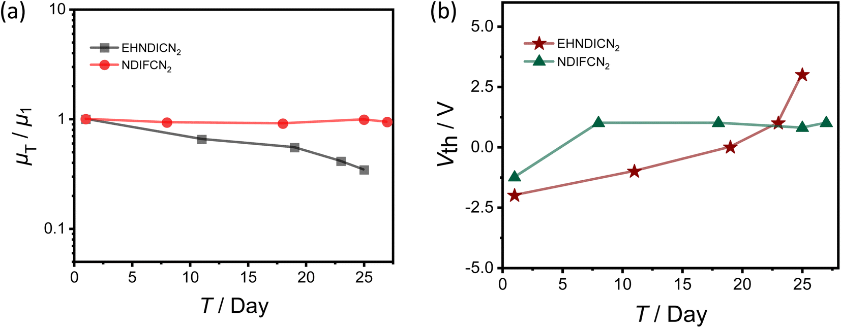 | ||
| Fig. 3 Ambient stability measurement: (a) relative mobility change of devices with exposure to the ambient atmosphere. (b) The threshold voltage changes (ΔVth) with time. | ||
| Deposition technique | µ maxe,sat (cm2 V−1 s−1) | V T (V) | I on/Ioff | Stability up to 10 days (retain) | |
|---|---|---|---|---|---|
| NDIFCN2 | Drop cast | 0.4 × 10⁻² | −1.25 | >103 | 94% |
| PVD | 1.6 × 10⁻² | 21 | 103 | ||
| EHNDICN2 | Spin-coat | 1.6 × 10⁻² | −2 | >104 | 66% |
| PVD | 4 × 10⁻² | 1.8 | 103 |
3.6. Film morphology
To understand the influence of the terminal alkyl chain on the morphology, atomic force microscope (AFM) and scanning electron microscope (SEM) analyses were carried out. The morphological studies (using SEM and AFM) of as-deposited NDIFCN2 and EHNDICN2 are summarised in Fig. 4. NDIFCN2 and EHNDICN2 films yielded pinhole-free uniform surface coverage with average root-mean-square roughness (Rq) of 2.4 and 2.8 nm, respectively.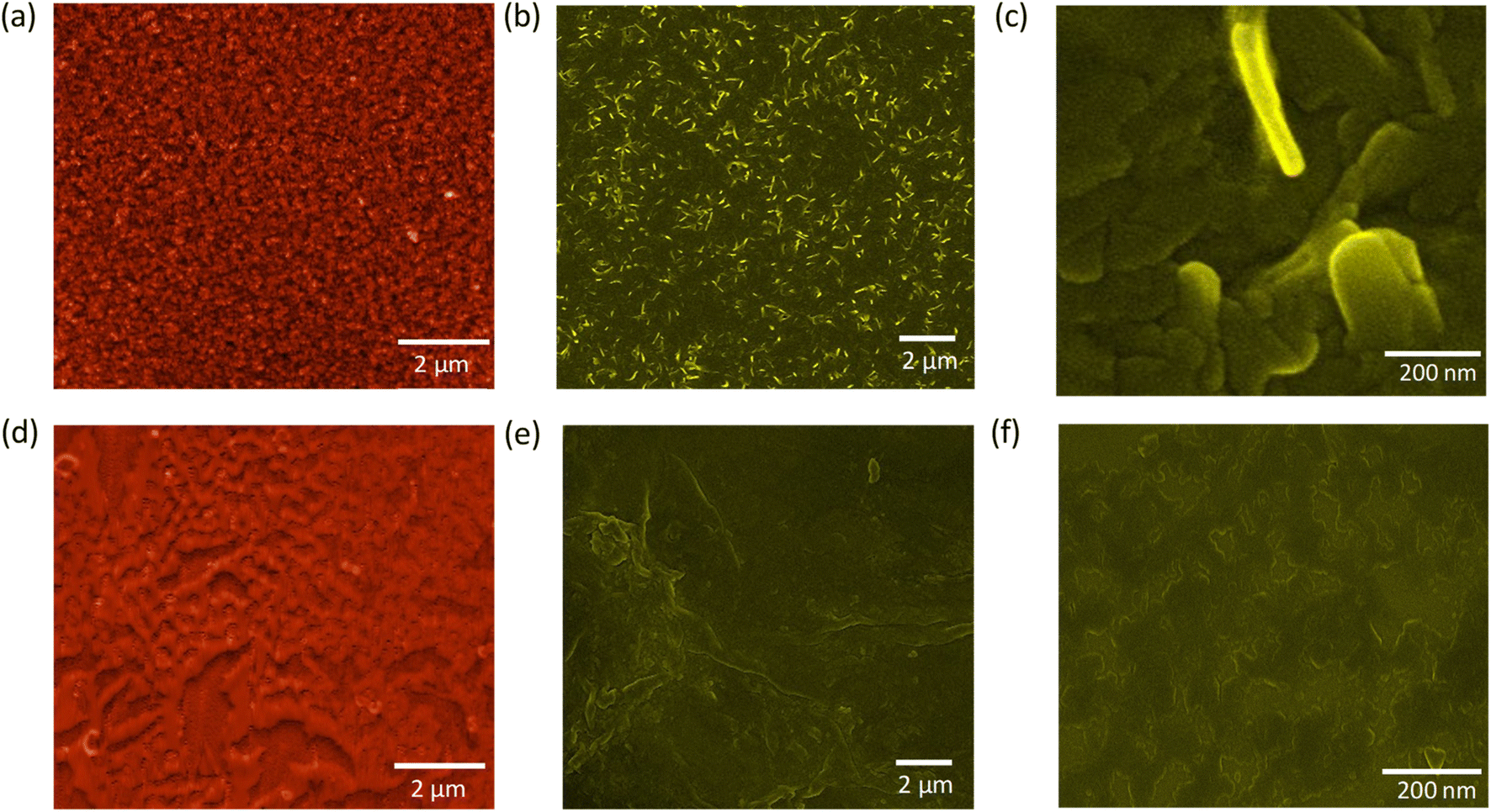 | ||
| Fig. 4 AFM images: (a) EHNDICN2 and (d) NDIFCN2; SEM images for EHNDICN2: scale (b) 2 µm and (c) 200 nm, for NDIFCN2: (e) 2 µm and (f) 200 nm. | ||
To elucidate the diverse electrical performances and to understand the in-plane and out-of-plane periodicity of bulk films deposited on substrates, 2D GIXRD (Grazing Incidence X-ray diffraction (https://measurlabs.com/methods/grazing-incidence-x-ray-diffraction-gixrd/)) measurements were conducted. EHNDICN2 film displayed distinct in-plane and out-of-plane (qz and qxy) ordering, as illustrated in (Fig. 5a and S14a†). In contrast, the NDIFCN2 films lacked both, confirming the amorphous nature of the films (Fig. 5b and S14b†). Distinct and periodic (00l) signals along qz were observed in the EHNDICN2 film (Fig. 5c), manifesting as higher-ordered peaks ranging from (001) to (004).
 | ||
| Fig. 5 2-D GIXRD diffraction profile of the samples: (a) EHNDICN2 and (b) NDIFCN2. 1-D line cut profile of the films (c) out-of-plane and (d) in-plane. (e) Film state WAXRD of both the samples. The schematic representation of deduced molecular orientation on the surface: (f) EHNDICN2 and (g) NDIFCN2. | ||
An edge-on molecular orientation (Fig. 5f) shall be expected, considering the molecular dimension and the d-spacing of the (00l) planes, where the conjugated backbones align perpendicular to the substrate, fostering favourable intermolecular π-stacking interactions. The qz d-spacing, derived from the (001) peak and measuring 15.8 Å, suggests that the molecular long axis was positioned with a significant tilt angle (considering the molecular length of 25.5 Å). The calculated minimum in-plane (qxy) d-spacing was 4.1 Å, indicating π–π stacking distances within the film's in-plane packing configuration. Wide-angle X-ray diffraction (WAXRD) measurements in the out-of-plane mode were also performed. For EHNDICN2, a preferential ordering along the 00l planes was visible (Fig. 5e), while films of NDIFCN2 samples display randomly oriented domains on the surface (Fig. 5g). XRD measurements substantiate that EHNDICN2 exhibits a more favourable orientation on the surface, facilitating electron transport in alignment with the carrier mobility extracted from the OFET devices.
4. Conclusions
We report ambient stable solution processable n-type OFET constituting core substituted NDI active layer molecules with symmetric alkyl and fluoroalkyl chain end groups. Core-substitution with –CN groups resulted in deeper LUMO (<−4.0 eV) in this pair of molecules. Apart from the deep LUMO, the end substitution of the NDI with fluoroalkyl chains (NDIFCN2) led to further lowering of LUMO compared to its alkyl derivative (EHNDICN2). Additionally, the fluoroalkyl group acts as a hydrophobic lamination layer to impart additional ambient stability to the active layers in their solution-processed OFETs (Scheme 2). Impressive ambient stability near 30 days at a relative atmospheric humidity (>65%) condition in the case of NDIFCN2 devices. Hence, the ambient stability of organic semiconductor devices needs to be addressed beyond the mere lowering of the LUMO level of the active layer materials. | ||
| Scheme 2 Schematic representation of the findings summarized in the article. | ||
Conflicts of interest
The authors declare no competing financial interest.Acknowledgements
The authors acknowledge the financial support from the IGSTC 2+2 grant (LABELONIK). IG is thankful to UGC for the research fellowship. RV acknowledge SERB for CRG/2021/006054. SPS acknowledges funding from DAE and SERB (SRG/2020/001641 and IPA/2021/000096). We acknowledge DESY (Hamburg, Germany), a member of the Helmholtz Association HGF, for the provision of experimental facilities. Parts of this research were carried out at the P08 beamline, PETRA III, DESY, Germany. Beamtime was allocated for proposal(s) (Project No. I-20221013, I-20211469). We acknowledge financial support by the Department of Science & Technology, Government of India (DST), provided within the framework of the India@Desy collaboration.References
- J. T. E. Quinn, J. Zhu, X. Li, J. Wangb and Y. Li, J. Mater. Chem. C, 2017, 5, 8654–8681 RSC.
- J. Chen, W. Zhang, L. Wang and G. Yu, Adv. Mater., 2023, 35, 2210772 CrossRef CAS PubMed.
- T. Yamamoto and K. Takimiya, J. Am. Chem. Soc., 2007, 129, 2224–2225 CrossRef CAS PubMed.
- H. Sirringhaus, Adv. Mater., 2014, 26, 1319–1335 CrossRef CAS PubMed.
- M. Kettner, Z. Mi, D. Kälblein, J. Brill, P. W. M. Blom and R. T. Weitz, Adv. Electron. Mater., 2019, 5, 1900295 CrossRef CAS.
- S. Vegiraju, G. Y. He, C. Kim, P. Priyanka, Y. J. Chiu, C. W. Liu, C. Y. Huang, J. S. Ni, Y. W. Wu, Z. Chen, G. H. Lee, S. H. Tung, C. L. Liu, M. C. Chen and A. Facchetti, Adv. Funct. Mater., 2017, 27, 1606761 CrossRef.
- B. B. J. Jung, K. Lee, J. Sun, A. G. Andreou and H. E. Katz, Adv. Funct. Mater., 2010, 20, 2930–2944 CrossRef CAS.
- F. Zhang, Y. Hu, T. Schuettfort, C. Di, X. Gao, C. R. McNeill, L. Thomsen, S. C. B. Mannsfeld, W. Yuan, H. Sirringhaus and D. Zhu, J. Am. Chem. Soc., 2013, 135, 2338–2349 CrossRef CAS PubMed.
- X. Gao, C. Di, Y. Hu, X. Yang, H. Fan, F. Zhang, Y. Liu, H. Li and D. Zhu, J. Am. Chem. Soc., 2010, 132, 3697–3699 CrossRef CAS PubMed.
- B. A. Jones, M. J. Ahrens, M. H. Yoon, A. Facchetti, T. J. Marks and M. R. Wasielewski, Angew. Chem., Int. Ed., 2004, 43, 6363–6366 CrossRef CAS PubMed.
- J. Soeda, T. Uemura, Y. Mizuno, A. Nakao, Y. Nakazawa, A. Facchetti and J. Takeya, Adv. Mater., 2011, 23, 3681–3685 CrossRef CAS PubMed.
- J. Chang, Q. Ye, K. Huang, J. Zhang, Z. Chen, J. Wu and C. Chi, Org. Lett., 2012, 14, 2964–2967 CrossRef CAS PubMed.
- Y. Kumar, S. Kumar, K. Mandal and P. Mukhopadhyay, Angew. Chem., Int. Ed., 2018, 130, 16556–16560 CrossRef.
- J. Dhar, U. Salzner and S. Patil, J. Mater. Chem. C, 2017, 5, 7404–7430 RSC.
- J. Ma, K. Hashimoto, T. Koganezawa and K. Tajima, J. Am. Chem. Soc., 2013, 135, 9644–9647 CrossRef CAS PubMed.
- M. Mas-Torrent and C. Rovira, Chem. Rev., 2011, 111, 4833–4856 CrossRef CAS PubMed.
- M. M. Payne, S. R. Parkin, J. E. Anthony, C. C. Kuo and T. N. Jackson, J. Am. Chem. Soc., 2005, 127, 4986–4987 CrossRef CAS PubMed.
- M. A. Stoeckel, Y. Olivier, M. Gobbi, D. Dudenko, V. Lemaur, M. Zbiri, A. A. Y. Guilbert, G. D'Avino, F. Liscio, A. Migliori, L. Ortolani, N. Demitri, X. Jin, Y. G. Jeong, A. Liscio, M. V. Nardi, L. Pasquali, L. Razzari, D. Beljonne, P. Samorì and E. Orgiu, Adv. Mater., 2021, 33, 2007870 CrossRef CAS PubMed.
- K. Liu, B. Ouyang, X. Guo, Y. Guo and Y. Liu, npj Flexible Electron., 2022, 6, 1 CrossRef CAS.
- Y. Yuan, G. Giri, A. L. Ayzner, A. P. Zoombelt, S. C. B. Mannsfeld, J. Chen, D. Nordlund, M. F. Toney, J. Huang and Z. Bao, Nat. Commun., 2014, 5, 723 Search PubMed.
- C. Luo, A. K. K. Kyaw, L. A. Perez, S. Patel, M. Wang, B. Grimm, G. C. Bazan, E. J. Kramer and A. J. Heeger, Nano Lett., 2014, 14, 2764–2771 CrossRef CAS PubMed.
- K. Takimiya, H. Ebata, K. Sakamoto, T. Izawa, T. Otsubo and Y. Kunugi, J. Am. Chem. Soc., 2006, 128, 12604–12605 CrossRef CAS PubMed.
- P. Kafourou, B. Park, J. Luke, L. Tan, J. Panidi, F. Glçcklhofer, J. Kim, T. D. Anthopoulos, J. S. Kim, K. Lee, S. Kwon and M. Heeney, Angew. Chem., Int. Ed., 2021, 60, 5970–5977 CrossRef CAS PubMed.
- T. Hodsden, K. J. Thorley, J. Panidi, A. Basu, A. V. Marsh, H. Dai, A. J. P. White, C. Wang, W. Mitchell, F. Glöcklhofer, T. D. Anthopoulos and M. Heeney, Adv. Funct. Mater., 2020, 30, 2000325 CrossRef CAS.
- W. Y. Lee, J. H. Oh, S. L. Suraru, W. C. Chen, F. Würthner and Z. Bao, Adv. Funct. Mater., 2011, 21, 4173–4181 CrossRef CAS.
- T. He, M. Stolte and F. Würthner, Adv. Mater., 2013, 25, 6951–6955 CrossRef CAS PubMed.
- K. J. Kalita, I. Giri and R. K. Vijayaraghavan, RSC Adv., 2021, 11, 33703–33713 RSC.
- J. Zaumseil and H. Sirringhaus, Chem. Rev., 2007, 107, 1296–1323 CrossRef CAS PubMed.
- J. Shukla and P. Mukhopadhyay, Eur. J. Org Chem., 2019, 2019, 7770–7786 CrossRef CAS.
- N. J. Hestand and F. C. Spano, Chem. Rev., 2018, 118, 7069–7163 CrossRef CAS PubMed.
- B. K. Barman, N. G. Ghosh, I. Giri, C. Kumar, S. S. Zade and R. K. Vijayaraghavan, Nanoscale, 2021, 13, 6759–6763 RSC.
- Z. A. Lamport, H. F. Haneef, S. Anand, M. Waldrip and O. D. Jurchescu, J. Appl. Phys., 2018, 124, 071101 CrossRef.
Footnote |
| † Electronic supplementary information (ESI) available: Structural characterization data, cyclic voltammetry, detailed device fabrication procedure, single crystal structural analysis, film morphology analysis, and contact angle measurement. CCDC 2241411 and 2176144. For ESI and crystallographic data in CIF or other electronic format see DOI: https://doi.org/10.1039/d4ra01499e |
| This journal is © The Royal Society of Chemistry 2024 |