
 Open Access Article
 This Open Access Article is licensed under a Creative Commons Attribution-Non Commercial 3.0 Unported Licence
Electrical performance of La-doped In2O3 thin-film transistors prepared using a solution method for low-voltage driving
Hongguo Duab,
Kamale Tuokedaerhan *ab and
Renjia Zhangab
*ab and
Renjia Zhangab
aXinjiang Key Laboratory of Solid State Physics and Devices, Xinjiang University, Urumqi 830046, China. E-mail: kamale9025@163.com
bThe School of Physics Science and Technology, Xinjiang University, Urumqi 830046, China
First published on 28th May 2024
Abstract
In this paper, La-doped In2O3 thin-film transistors (TFTs) were prepared by using a solution method, and the effects of La doping on the structure, surface morphology, optics, and performance of In2O3 thin films and TFTs were systematically investigated. The oxygen defects concentration decreased from 27.54% to 17.93% when La doping was increased to 10 mol%, and La served as a carrier suppressor, effectively passivating defects such as oxygen defects. In fact, the trap density at the dielectric/channel interface and within the active layer can be effectively reduced using this approach. With the increase of La concentration, the mobility of LaInO TFTs decreases gradually; the threshold voltage is shifted in the positive direction, and the TFT devices are operated in the enhanced mode. The TFT device achieved a subthreshold swing (SS) as low as 0.84 V dec−1, a mobility (μ) of 14.22 cm2 V−1 s−1, a threshold voltage (VTH) of 2.16 V, and a current switching ratio of Ion/Ioff of 105 at a low operating voltage of 1 V. Therefore, regulating the doping concentration of La can greatly enhance the performance of TFT devices, which promotes the application of such devices in high-performance, large-scale, and low-power electronic systems.
1. Introduction
Given their high carrier mobility, superior optical transmittance, low processing temperature, high uniformity, and exceptional environmental stability, metal oxide semiconductors have been the subject of extensive research. Researchers have also applied metal oxides to thin-film transistors, which can enable large-area, high-resolution displays. For example, metal oxides such as ZnO,1 In2O3,2 GZO,3 and IZGO,4 have been extensively studied. Among these materials In2O3 is a highly representative material. It has high mobility because of overlapping In 5s orbitals5,6 and has a wide bandgap and high transparency compared with conventional amorphous silicon. Moreover, amorphous metal oxides are highly deformable, and they can be used to fabricate wearable transparent flexible electronic devices on flexible substrates.7However, In2O3 TFTs suffer from a series of problems such as high carrier concentration and defects such as oxygen defects, which lead to a low current switching ratio and poor stability of In2O3 TFTs under voltage, light and other conditions.8 Thus, researchers have proposed many methods to improve the performance of In2O3 TFTs. For example, the performance of TFTs has been improved by selecting suitable dopants as carrier suppressors such as Tb,9 B,10 Sr,11 and Ni.12
Standard electrode potential (SEP), electronegativity and the ability to bind oxygen are the main criteria for selecting a suitable dopant.13,14 Notably, a dopant with a low SEP, low electronegativity, and strong oxygen-binding ability contributes to the stability and performance of TFTs.8,15 Among these dopants, La is selected as a dopant in this paper. First, the band gap of lanthanum oxide (La2O3, ∼5.5 eV) is larger than that of In2O3 (∼3.6 eV), and the SEP of La (−2.37 V) is lower than that of indium (−0.33 V).16 In addition, the bonding energy of the La–O bond is 798 kJ mol−1, which is larger than that of the In–O bond (346 kJ mol−1). The formation of oxygen defects and hydroxyl groups can be reduced while controlling the carrier concentration. Moreover, the La3+ ion has the same valence state as the In3+ ion. Therefore, the doping of La3+ ions in In2O3 does not produce additional carriers.17 Furthermore, La is a good dopant to increase the performance of In2O3 TFTs.
Most high-performance TFTs are prepared by RF magnetron sputtering,18 atomic layer deposition,19,20 pulsed laser method,21,22 and molecular beam epitaxy.23–26 These methods are expensive and difficult to prepare, and they require vacuum conditions. By contrast, the solution method has a simpler process, and lower manufacturing costs without the need for vacuum conditions, and this method can achieve large-area deposition. In addition, the solution method is considered a sustainable processing method.
Here, La-doped In2O3 TFTs were created using a solution method, and the mechanism by which the microstructure, optical characteristics, and electrical characteristics of the films were affected by 0 mol%–10 mol% La doping were examined. The results indicate that the doping of La reduces the content of oxygen defects and enhances the electrical performance of TFTs.
2. Experimental details
A total of 0.1 moles of indium nitrate hydrate (In(NO3)3·xH2O) and lanthanum nitrate hexahydrate (La(NO3)3·6H2O) were dissolved in 2-methoxyethanol, with varying La![[thin space (1/6-em)]](https://www.rsc.org/images/entities/char_2009.gif) :In ratios of 0 mol%, 1 mol%, 3 mol%, 5 mol%, and 10 mol%. In addition, ammonia and acetylacetone were added to the precursor solution as a fluxing agent and stirred for 6 h until the solution was clear and transparent. Finally, the solution was left to age for a period of time at room temperature to obtain a stable precursor solution.
:In ratios of 0 mol%, 1 mol%, 3 mol%, 5 mol%, and 10 mol%. In addition, ammonia and acetylacetone were added to the precursor solution as a fluxing agent and stirred for 6 h until the solution was clear and transparent. Finally, the solution was left to age for a period of time at room temperature to obtain a stable precursor solution.
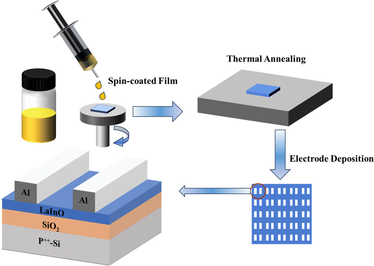
The substrate must be cleaned before depositing the film. P(100)-type Si was selected as the substrate, which has a resistivity of 0.005 Ω cm with 100 nm SiO2. The substrate was sequentially sonicated through acetone, anhydrous ethanol and deionized water for 15 min to clean the surface of the wafer from impurities such as organic matter and grease. Finally, it was treated with plasma for 1 min to increase hydrophilicity. The precursor solution was filtered via a 0.22 μm injection filter before being spun coated to generate a purer precursor solution. Spin coating was performed at 5000 rpm for 30 s at room temperature and then placed on a heating table at 150 °C for 5 min. This method was repeated two times to obtain the desired thickness. Afterward, LaInO films were produced by annealing for an hour at 500 °C in the air. Finally, the source and drain electrodes were deposited using the shadow mask plate technique with an electrode thickness of approximately 30 nm. The detailed preparation process of LaInO films as well as LaInO TFTs is shown in Fig. 1.
 | ||
| Fig. 1 Flowchart for the preparation of LaInO TFTs by using the solution method. | ||
The electrical performance of TFTs was tested using a semiconductor parameter analyzer (Keysight B1500A). The crystallographic information of the films was analyzed using X-ray diffraction (XRD, Bruker D8 Advance). The chemical state and structure of the films were characterized using X-ray photoelectron spectroscopy (XPS, Thermo scalable 250 Xi). The surface morphology of the films was analyzed using an atomic force microscope (Bruker Dimension Icon). The surface and cross-section of the films were characterized by field-emission scanning electron microscopy (SEM, SU8020). The optical properties of the films were tested by using an ultraviolet-visible spectrophotometer (UV-Vis). Finally, the energy band structure of the films was analyzed.
3. Results and discussion
Fig. 2 shows the XRD patterns of In2O3 and LaInO films with different doping concentrations. As shown in the figure, the film has (222), (400), (440), and (622) crystal planes, and the corresponding diffraction angles 2θ are 30.58°, 35.46°, 51.03°, and 60.67°, respectively. The grain size was calculated on the basis of the Debye–Scherrer equation:27
 | (1) |
 | ||
| Fig. 2 XRD pattern of thin-film LaInO. | ||
Fig. 3(a) and (b) shows the SEM surface and cross-section images of the InLaO-5% film. Based on the figure, the surface of the LaInO film is smooth, uniform, and dense, and the thickness of the film is approximately 25 nm. The thickness of the film can affect the electrical properties of the TFT, with an exponential decrease in carrier surface scattering mobility because of the thickness of the film below a critical value of approximately 10 nm.28 Jozeph Park et al. showed that a 20 nm thick active layer had the best mobility and demonstrated that the mobility progressively deteriorated with the decrease of thickness.29 Therefore, we controlled the film thickness was controlled to 25 nm. A clear interfacial separation between the LaInO layer and the substrate can also be seen in the inset, which indicates that no diffusion between the film and the substrate is has occurred.
 | ||
| Fig. 3 SEM surface images (a) and (b) cross-sectional images of LaInO-5% films. | ||
Fig. 4 displays an image obtained using atomic force microscopy (AFM) of the LaInO thin film, with a scanning range of 2 μm × 2 μm. The films that were annealed at 500 °C and doped at of 0 mol%, 1 mol%, 3 mol%, 5 mol%, and 10 mol% had root-mean-square roughness values of 0.574, 0.536, 0.463, 0.527, and 0.783 nm, respectively. The roughness of all the films is less than 1 nm, which indicates that the films are smooth and uniform. As the doping concentration increases, the roughness initially decreases, which is due to the fact that the homogeneous diffusion of atomic clusters can be promoted by proper doping of La. However, excessive doping leads to an increase in roughness, which may be due to the fact that the radius of La ions (106.1 pm) is larger than the radius of In ions (80 pm), resulting in the difficult embedding of La ions in the In2O3 lattice, moreover, with the increase of La content, roughness increases with the increase of film defects. Smooth films are important for high-performance metal oxide TFTs, indicating their advantages of solution processing.
 | ||
| Fig. 4 AFM images of LaInO films with different doping ratios: (a) 0 mol%, (b) 1 mol%, (c) 3 mol%, (d) 5 mol%, and (e) 10 mol%. | ||
XPS analysis was performed to analyze the chemical structure of the films. As shown in Fig. 5(a)–(e), all O1s peaks are calibrated by the C1s peak (284.8 eV). The O1s peaks of the LaInO films were divided into three peaks: OM (529.6 eV), OV (530.9 eV), and OH (532.1 eV). OM indicates lattice oxygen, which refers to the bonds between metal atoms and oxygen atoms. OV represents oxygen vacancies, which are vacant positions where oxygen atoms are missing in the lattice. OH denotes bound oxygen, which is related to the adsorption of O2, H2O, and –CO3 on the surface.30 Free electrons are produced from oxygen defects, indicating the importance of OV. The ratio of OV/(OM + OV + OH) was calculated. As shown in Fig. 5(f), the ratio of OV/(OM + OV + OH) in LaInO films with increasing La doping is 27.54%, 27.07%, 24.02%, 19.07%, and 17.93%. Based on the abovementioned analysis, the addition of La can inhibit the generation of oxygen defects in the film and reduce the defects in the LaInO film. Oxygen defects can provide additional electrons to oxide semiconductors. However, if elemental La is doped into In2O3 to reduce oxygen defects, then electron concentration decreases.
 | ||
| Fig. 5 XPS patterns of the thin films of O1s at (a) 0 mol%, (b) 1 mol%, (c) 3 mol%, (d) 5 mol%, and (e) 10 mol%. (f) Percentage of OV varying with different doping ratios. | ||
The XPS patterns of In3d and La3d are shown in Fig. 6(a) and (b). The In3d energy-level spin orbital splits into In3d3/2 and In3d5/2 peaks corresponding to peaks centered at 451.8 eV and 444.28 eV at 0 mol% doping, respectively. With the increase of doping, the peak of In3d is gradually shifted toward a lower binding energy because the bond energy of the La–O bond (798 kJ mol−1) is greater than that of the In–O bond (346 kJ mol−1), which will combine with oxygen to form more metal–oxygen bonds. Therefore, the oxygen defects can be reduced to lower the trap state density, which improves the performance of the TFTs.16 The La3d energy level spin orbital splits into La3d3/2 and La3d5/2 peaks. Their main peaks are located at 851.5 eV and 834.6 eV, respectively. With the increase of La3+ doping, the peak intensity is gradually enhanced, indicating that La3+ is completely doped into the In2O3 film.
 | ||
| Fig. 6 (a) XPS profile of In3d, and (b) XPS profile of La3d. | ||
The transfer characteristic (IDS–VGS) curve of La-doped In2O3 TFTs is shown in Fig. 7(a). The TFT devices were tested at room temperature using a Lake Shore TTPX probe stage and an Agilent semiconductor parameter analyzer at a source-drain voltage (VDS) of 1 V and a gate voltage (VGS) ranging from −40 V to +40 V. As shown in the figure, the curve is shifted in the positive direction as the amount of La doping increases, indicating that La doping leads to a decrease in the conductivity of the active layer.31 The addition of La suppressed the concentration of oxygen defects, which led to a decrease in carrier concentration and a shift in the curve's positive orientation. The electrical performance parameters of the TFTs are summarized in Table 1, which are all extracted from the transfer characteristic (IDS–VGS) curves. Among them, VTH is obtained by fitting the transfer characteristic (IDS–VGS) curve to obtain the IDS1/2–VGS curve. The VTH value is the junction point of the linear part's tangent and the horizontal axis VGS. The value of μ for all TFTs is calculated as follows:32
 | (2) |
 | ||
| Fig. 7 (a) Transfer characteristic curves at different La-doping concentrations (VDS = 1 V), (b) output characteristic curves for pure In2O3, and (c) output characteristic curves for La doping concentration of 5 mol%. | ||
| La-doping ratio (%) | μ (cm2 V−1 s−1) | VTH (V) | SS (V dec−1) | Ion/Ioff | Dit (cm−2 eV−1) |
|---|---|---|---|---|---|
| 0 | 28.14 | 1.08 | 1.45 | 104 | 1.55 × 10¹³ |
| 1 | 21.52 | 1.34 | 0.97 | 104 | 1.03 × 10¹² |
| 3 | 16.74 | 1.68 | 0.87 | 104 | 9.23 × 10¹² |
| 5 | 14.22 | 2.16 | 0.84 | 105 | 8.91 × 10¹² |
| 10 | 5.63 | 5.71 | 0.51 | 105 | 5.32 × 10¹² |
The μ value of pure In2O3 TFTs was obtained as 28.14 cm2 V−1 s−1 by performing calculations using the abovementioned equation. With the increase of La doping to 10 mol%, μ decreased from 28.14 cm2 V−1 s−1 to 5.63 cm2 V−1 s−1, and VTH increased from 1.08 V to 5.71 V. VTH is shifted in the positive direction and the TFT device is in the enhanced mode of operation. The current switching ratio is increased from 104 to 105, indicating an increase of one order of magnitude in Ion/Ioff compared with pure-phase In2O3 TFTs. The increase in Ion/Ioff was also attributed to the suppression of VO. The oxide semiconductor conduction theory states that a drop in carrier concentration causes μ to fall and VTH to increase.13 With the increase of La doping, the production of oxygen defects is suppressed. Oxygen defects are usually generated because of the dehydration and condensation of hydroxyl groups when oxide semiconductor films are solution treated.33 This result is due to the fact that the binding capacity of La to O is stronger than the binding energy of In to O. Therefore, the oxygen defects can be decreased by La doping, which lowers the charge concentration and influences μ and VTH. This finding is consistent with the earlier XPS examination. In addition, Ne was estimated as follows:34
 | (3) |
 | (4) |
The SS values were 1.45, 0.97, 0.87, 0.84 and 0.51 V dec−1 when the doping amount was 0 mol%, 1 mol%, 3 mol%, 5 mol% and 10 mol%, respectively. The SS value responds to the ability of TFTs to switch quickly. With the increase of La doping, the SS value decreases gradually, and the TFT performance is improved. This finding is associated with the decrease in oxygen vacancies and hydroxyl groups. The result demonstrates that La doping is an effective method to increase the TFT performance. SS is closely related to the density of trap states (Dit) at the interface between the insulating and active layers, and the Dit value can be estimated from the SS value using the following formula:36
 | (5) |
Fig. 8(a) displays the optical characteristics of thin-film samples. The transmittance of the films was tested by using a UV-Vis spectrophotometer. The films have a transmittance of over 90% in the visible range. High transparency is important for the fabrication of transparent devices, which proves its potential application value in the fabrication of transparent electronic devices. Considering that doping elements may cause changes in the energy band structure, we have systematically studied them. The inset shows the optical band gap (Eg) profiles of In2O3 films and LaInO films at 5 mol% doping. The transmission spectra were fitted to the data using the following standard Tauc plot formula: αhν = A(hν − Eg)1/2,39 where α is the absorbance index, h and ν are the Planck's constant and frequency, respectively, and A is the constant. The Eg value of the In2O3 film is 3.63 eV, whereas the addition of La increases the Eg value to 3.72 eV. La–O has a higher binding energy than In–O. Thus, as the amount of La doping increases, the oxygen vacancy defects are eliminated, leading to an increase in bandgap. In addition, the band gap of lanthanum oxide (La2O3) is larger (∼5.5 eV) than that of In2O3 (∼3.6 eV). Thus, La-doping results in a larger optical band gap. As shown in Fig. 8(b), the valence band maxima (EV) were taken from the XPS valence band spectra of In2O3 and LaInO (5 mol%) films, from which the conduction band minima (EC) and the Fermi energy levels (EF) were estimated. The energy band structures of In2O3 and LaInO (5 mol%) films are shown in Fig. 8(c). The EV value of In2O3 and LaInO (5 mol%) films was 2.74 eV and 2.78 eV, respectively. A slight increase in EV was observed after La doping compared with pure In2O3. The conduction band offset is calculated as follows: ΔECB = Eg − EVB. The ECB of In2O3 and LaInO (5 mol%) films were 0.89 and 0.94 eV, respectively. According to semiconductor physics, the carrier concentration Ne can be estimated from ΔECB using the following equation40
| Ne = NCe(−ECB/KT) | (6) |
 | ||
| Fig. 8 (a) Optical transmittance of LaInO films. The inset shows the optical band gap of pure In2O3 and LaInO-5% films, (b) valence band mapping of pure In2O3 and LaInO-5% films, and (c) energy band structure of pure In2O3 and LaInO-5% films. | ||
4. Conclusions
In this study, LaInO thin films and LaInO TFTs were prepared using the solution method with La as the dopant. The microstructure of LaInO thin films with different doping concentrations and the electrical properties of the devices were investigated. XRD analysis shows that La doping can increase the crystallization temperature of In2O3. The AFM and SEM images show that the films prepared by the solution method are smooth and uniform, and the roughness is less than 1 nm, which is an ideal material to be used as the active layer of TFT. The XPS analysis results show that La doping can suppress the oxygen defects inside the film because that La has a low SEP (−2.37 V) and a large bond energy of the La–O bond (798 kJ mol−1), which can serve as a carrier suppressor in thin films. Electrical tests show that moderate amount of La doping can effectively improve the Ion/Ioff, VTH, and SS values of TFT devices. The best performance of the device was achieved when La doping was 5 mol%, driven by a low voltage of 1 V with μ = 14.22 cm2 V−1 s−1, VTH = 2.16 V, SS = 0.84 V dec−1, and Ion/Ioff = 105. Therefore, LaInO thin films prepared by the solution method are considered as promising next-generation good active layer materials for TFTs with great application potential in future low-cost, low-power and large-area oxide electronic devices.Conflicts of interest
There are no conflicts to declare.Acknowledgements
This research was supported by the Natural Science Foundation of Xinjiang Uygur Autonomous Region (Grant No. 2021D01C035), the National Natural Science Foundation of China (Grant No. 62141402).References
- A. Abliz, D. Wan, L. Yang, M. Mamatrishat Mamat, H. Chen, L. Xu, C. Wang and H. Duan, Mater. Sci. Semicond. Process., 2019, 95, 54–58 CrossRef CAS.
- J. H. Noh, S. Y. Ryu, S. J. Jo, C. S. Kim, S.-W. Sohn, P. D. Rack, D. J. Kim and H. K. Baik, IEEE Electron Device Lett., 2010, 31, 567–569 CAS.
- D. Zhu, Q. Wang, S. Han, P. Cao, W. J. Liu, F. Jia, Y. Zeng and X. Ma, Appl. Surf. Sci., 2014, 298, 208–213 CrossRef CAS.
- A. Abliz, Q. Gao, D. Wan, X. Liu, L. Xu, C. Liu, C. Jiang, X. Li, H. Chen, T. Guo, J. Li and L. Liao, ACS Appl. Mater. Interfaces, 2017, 9, 10798–10804 CrossRef CAS PubMed.
- J. Sheng, H. J. Jeong, K. L. Han, T. Hong and J. S. Park, J. Inf. Disp., 2017, 18, 159–172 CrossRef CAS.
- W. Xu, T. Peng, S. Zhuo, Q. Lin, W. Huang, Y. Li, F. Xu, C. Zhao and D. Zhu, Int. J. Mol. Sci., 2022, 23, 12912 CrossRef CAS PubMed.
- L. Petti, N. Münzenrieder, C. Vogt, H. Faber, L. Büthe, G. Cantarella, F. Bottacchi, T. D. Anthopoulos and G. Tröster, Applied Physics Reviews, 2016, 3, 021303 CrossRef.
- L. Hong, W. Xu, W. Liu, S. Han, P. Cao, M. Fang, D. Zhu and Y. Lu, Appl. Surf. Sci., 2020, 504, 144499 CrossRef CAS.
- P. He, R. Hong, G. Li, X. Zou, W. Hu, L. Lan, B. Iñiguez, L. Liao and X. Liu, IEEE Electron Device Lett., 2022, 43, 1894–1897 CAS.
- W. Xu, T. Peng, Y. Li, F. Xu, Y. Zhang, C. Zhao, M. Fang, S. Han, D. Zhu, P. Cao, W. Liu and Y. Lu, Nanomaterials, 2022, 12, 1125 CrossRef CAS PubMed.
- Y. Zhou, J. Li, D. Y. Zhong, X. Li and J. Zhang, IEEE Trans. Electron Devices, 2019, 66, 1308–1313 CAS.
- Y. Li, W. Xu, W. Liu, S. Han, P. Cao, M. Fang, D. Zhu and Y. Lu, ACS Appl. Electron. Mater., 2019, 1, 1842–1851 CrossRef CAS.
- S. Lee, T. H. Kim, J. H. Lee, C. Avis and J. Jang, Appl. Phys. Lett., 2017, 110, 122102 CrossRef.
- W. Song, L. Lan, M. Li, L. Wang, Z. Lin, S. Sun, Y. Li, E. Song, P. Gao, Y. Li and J. Peng, J. Phys. D: Appl. Phys., 2017, 50, 385108 CrossRef.
- C. J. Zhao, J. Li, D. Y. Zhong, C. X. Huang, J. Zhang, X. Li, X. Y. Jiang and Z. Zhang, IEEE Trans. Electron Devices, 2017, 64, 2216–2220 CAS.
- C. J. Zhao, J. Li, D. Y. Zhong, C.-X. Huang, J. Zhang, X. Li, X. Y. Jiang and Z. Zhang, IEEE Trans. Electron Devices, 2018, 65, 526–532 CAS.
- Z. Lin, L. Lan, S. Sun, Y. Li, W. Song, P. Gao, E. Song, P. Zhang, M. Li, L. Wang and J. Peng, Appl. Phys. Lett., 2017, 110, 133502 CrossRef.
- G. Gonçalves, P. Barquinha, L. Pereira, N. Franco, E. Alves, R. Martins and E. Fortunato, Electrochem. Solid-State Lett., 2010, 13, H20 CrossRef.
- H. J. Jeong, Y. S. Kim, S. G. Jeong and J. S. Park, ACS Appl. Electron. Mater., 2022, 4, 1343–1350 CrossRef CAS.
- J. zhen Sheng, E. J. Park, B. Shong and J. S. Park, ACS Appl. Mater. Interfaces, 2017, 9, 23934–23940 CrossRef PubMed.
- T. Itoh, A. Kobayashi, K. Ueno, J. Ohta and H. Fujioka, Sci. Rep., 2016, 6, 29500 CrossRef CAS PubMed.
- V. H. Martínez-Landeros, N. Hernández-Como, G. Gutierrez-Heredia, R. Ramírez-Bon, M. A. Quevedo-López and F. S. Aguirre-Tostado, Semicond. Sci. Technol., 2019, 34, 025008 CrossRef.
- X. A. Zhang, J. W. Zhang, W. F. Zhang, D. Wang, Z. Bi, X. M. Bian and X. Hou, Thin Solid Films, 2008, 516, 3305–3308 CrossRef CAS.
- H. Huang, F. J. Liu, J. Sun, J. Zhao, Z. Hu, Z. J. Li, X. Q. Zhang and Y. Wang, Appl. Surf. Sci., 2011, 257, 10721–10724 CrossRef CAS.
- X. Zhang, J. Zhang, W. Zhang and X. Hou, Semicond. Sci. Technol., 2010, 25, 045026 CrossRef.
- Y. Zhang, A. Neal, Z. Xia, C. Joishi, J. M. Johnson, Y. Zheng, S. Bajaj, M. Brenner, D. Dorsey, K. Chabak, G. Jessen, J. Hwang, S. Mou, J. P. Heremans and S. Rajan, Appl. Phys. Lett., 2018, 112, 173502 CrossRef.
- J. U. Bhanu and P. Thangadurai, Mater. Sci. Semicond. Process., 2020, 119, 105171 CrossRef CAS.
- I. Isakov, H. Faber, A. D. Mottram, S. Das, M. Grell, A. Regoutz, R. Kilmurray, M. A. McLachlan, D. J. Payne and T. D. Anthopoulos, Adv. Electron. Mater., 2020, 6, 2000682 CrossRef CAS.
- J. Park, Y. S. Kim, J. H. Kim, K. Park, Y. C. Park and H.-S. Kim, J. Alloys Compd., 2016, 688, 666–671 CrossRef CAS.
- A. Abliz, L. Xu, D. Wan, H. Duan, J. Wang, C. Wang, S. Luo and C. Liu, Appl. Surf. Sci., 2019, 475, 565–570 CrossRef CAS.
- W. Wang, G. He, H. Yu, Q. Gao, L. Wang, X. Xu, Y. Zhang, X. Wu and B. He, Phys. Status Solidi A, 2022, 219, 2100590 CrossRef CAS.
- T. Kamiya, K. Nomura and H. Hosono, Sci. Technol. Adv. Mater., 2010, 11, 044305 CrossRef PubMed.
- J. Chil, H. B. Kim, C. H. Ahn, H. K. Cho and H. S. Lee, J. Mater. Res., 2012, 27, 2293–2298 CrossRef.
- J. Han, A. Abliz and D. Wan, Chin. J. Phys., 2022, 77, 327–334 CrossRef CAS.
- Q. Chen, J. Li, Y. Yang, W. Zhu and J. Zhang, Nanotechnology, 2019, 30, 425205 CrossRef CAS PubMed.
- J. S. Park, W. J. Maeng, H. S. Kim and J. S. Park, Thin Solid Films, 2012, 520, 1679–1693 CrossRef CAS.
- C. C. Ting, H. Y. Fan, M. K. Tsai, W. Li, H. E. Yong and Y. H. Lin, Phys. Status Solidi A, 2013, 211, 800–810 CrossRef.
- S. Arulkumar, S. Parthiban, D. Gnanaprakash and J. Y. Kwon, J. Mater. Sci.: Mater. Electron., 2019, 30, 18696–18701 CrossRef CAS.
- H. Cai, K. Tuokedaerhan, Z. Lu, R. Zhang and H. Du, Vacuum, 2023, 217, 112542 CrossRef CAS.
- T. Kamiya, K. Nomura and H. Hosono, J. Disp. Technol., 2009, 5, 462–467 CAS.
| This journal is © The Royal Society of Chemistry 2024 |