
 Open Access Article
 This Open Access Article is licensed under a Creative Commons Attribution-Non Commercial 3.0 Unported Licence
The impact of thickness-related grain boundary migration on hole concentration and mobility of p-type transparent conducting CuI films
Ruibin Xue a,
Gang Gao*a,
Lei Yangb,
Liangge Xua,
Yumin Zhang*a and
Jiaqi Zhuacd
a,
Gang Gao*a,
Lei Yangb,
Liangge Xua,
Yumin Zhang*a and
Jiaqi Zhuacd
aNational Key Laboratory of Science and Technology on Advanced Composites in Special Environments, Harbin Institute of Technology, Harbin 150080, P. R. China. E-mail: gaogang@hit.edu.cn; zhym@hit.edu.cn
bCenter of Analysis Measurement, Harbin Institute of Technology, Harbin 150001, P. R. China
cZhengzhou Research Institute, Harbin Institute of Technology, Zhengzhou 450046, P. R. China
dKey Laboratory of Micro-systems and Micro-structures Manufacturing Ministry of Education, Harbin Institute of Technology, Harbin 150080, P. R. China
First published on 18th March 2024
Abstract
CuI films present promising optoelectronic properties for transparent conductors. However, the high hole concentration in CuI films hinders the controllable modulation of hole mobility, limiting their application in low-dimensional thin-film transistors. In this study, CuI films were prepared through a Cu film iodination method at room temperature, and a systematic investigation was conducted on the modulation of hole concentration and mobility with varying film thickness. The films exhibited a zinc blende structure (γ-phase) with increasing grain size as the thickness increased. The transmittance and optical bandgap of the films decreased with increasing thickness. The correlation of vacancy concentration with changing film thickness was analyzed through photoluminescence spectroscopy, revealing the influence of grain boundary migration on vacancy formation. The reduction in film thickness diminishes the migration of CuI grain boundaries, consequently reducing the probability of Cu vacancy and I vacancy formation, resulting in diminished hole concentration and enhanced hole mobility and film conductivity. The film with a thickness of 20 nm demonstrated optimal performance, with a transmittance of 90%, hole concentration of 4.09 × 1017 cm−3, hole mobility of 506.50 cm2 V−1 s−1, and conductivity of 33.19 S cm−1. This work deepens the understanding of hole transport such as hole concentration and mobility modulation in CuI films, highlighting the importance of controlling grain boundary migration during the film growth process.
1. Introduction
Thin-film transistors (TFTs) based on wide-bandgap transparent oxide semiconductors have attracted great research interest.1 For example, TFTs based on n-type amorphous indium–gallium–zinc oxide (IGZO) have been used in active-matrix flat panel displays, owing to their high field-effect mobility exceeding 10 cm2 V−1 s−1, excellent transparency, and low leakage current.2 However, the development of p-type TFTs has been comparatively slow due to the challenge of obtaining high-performance p-type semiconductors. P-channel TFTs are crucial components in complementary circuits. Despite some cutting-edge research achieving p-type TFTs based on oxide semiconductors like Cu2O,3 NiO,4 and SnO,5 their application in industrial settings remains challenging due to their inferior hole transport properties and chemical stability.6In p-type oxide semiconductors, the main component constituting the valence band maximum (VBM) is the strongly localized O 2p states, which results in a large effective mass of holes and therefore a hole mobility of less than 10 cm2 V−1 s−1.6 In the case of p-type doping of oxides, self-compensation occurs simultaneously because of the presence of intrinsic oxygen vacancy defects, for example, p-doped ZnO can easily convert to n-type conductivity.7 Recent studies have found that copper-based oxides have good hole transport capabilities, such as CuMO2 (M = B, Al, Cr, Ga, Sc, In and Y),8–13 SrCu2O2,14 and LnCuOCh (Ln = lanthanide, Ch = S, Se, Te).15,16 The VBM of copper-based oxides consists of O 2p states and Cu 3d states. The modulation of the Cu 3d states weakens the localization of the VBM, resulting in a reduction of the effective mass of the holes and a higher hole mobility.17 However, copper-based oxides have poor light transmission.18,19 Moreover, the preparation temperature of copper-based oxides is higher than 400 °C, which will undoubtedly result in higher process costs and lower production efficiency.20 Therefore, the development of high visible-light transmission p-type semiconductors with low temperature preparation routes for practical large-scale applications is the key to solving the shortage of p-channel TFTs.
Recently, CuI with a wide band gap of 3.1 eV has been considered by researchers as a promising material that can achieve high visible-light transmission and high p-type conductivity.21 Its VBM consists of I 5p and Cu 3d states.22,23 Because iodine has a larger p-orbital and smaller electronegativity than oxygen,24 it favours a low localized VBM, resulting in a small effective mass of holes (mh = 0.3m0, where m0 is the free electron mass) and a high hole mobility (∼43.9 cm2 V−1 s−1 in single crystal).25 The intrinsic p-type conductivity of CuI is derived from the shallow acceptor state Cu vacancies above the VBM and provides a hole concentration of 1019–1020 cm−3.26–28 Because of its good p-type conductivity, CuI has been investigated for TFTs,29,30 thermoelectric devices,31,32 solar cells,33,34 and photodetectors,35,36 and so on. CuI can be prepared using a variety of low temperature processes, including magnetron sputtering,37 thermal evaporation,38 pulsed laser deposition,39 solid state iodination and solution processes.40–42 These advantages make CuI suitable for flexible electronics.31,35
However, when CuI films are used in TFTs will result in a lower on/off current, because of the relatively high hole concentration.29,30,43 And the electrical properties of CuI films are difficult to control, as samples prepared by different processes have different properties due to deviations in stoichiometry. Despite research achieving the modulation of hole concentration in CuI films within the range of 1016–1019 cm−3 through doping with metallic elements or oxide, such as Zn2+, Sn4+, Cu2O.30,44,45 However, as devices move toward higher integration, the demand for thinner channel layers in TFTs increases.46 The non-uniformity of doping causes significant variations in local electrical properties in ultra-thin films, severely impacting device performance.47,48 Therefore, intrinsic p-type semiconductors exhibit clear advantages in low-dimensional applications. Understanding the variation in the optoelectronic properties of intrinsic CuI films with thickness is fundamental for comprehending and controlling carrier transport in these materials.
In this paper, we prepared CuI films of varying thickness through Cu films iodination at room temperature. The morphological structure, optical properties, hole transport performance, and defect concentration in correlation with film thickness were comprehensively revealed. Our results enhance the understanding of the hole transport mechanisms of CuI films, providing a theoretical basis for the modulation of hole transport in devices such as TFTs.
2. Experimental section
2.1 Materials
Cu target (99.99% purity) was purchased from Yipin Chuancheng Technology Co., Ltd (China). Ar (99.999% purity) was purchased from LIMING GAS (China). Iodine (99.8% purity), acetone (99.5% purity) and ethanol (99.5% purity) were purchased from Aladdin (China).2.2 Preparation of CuI films
Quartz substrates (10 × 10 × 1 mm) were ultrasonically cleaned with acetone and ethanol for 15 min, respectively. CuI films were prepared through a Cu film iodination process. The method comprises two steps: first, the deposition of Cu films, followed by the iodination of the Cu films, with all processes conducted at room temperature without heating. The Cu films were deposited on cleaned quartz substrates using a direct current (DC) magnetron sputtering system, and Ar was employed as the sputtering gas. First, the Cu target and the substrates were inserted into the sputtering system, and the substrates were shielded with a blocker. Then, the sputtering chamber was evacuated to 5 × 10⁻⁴ Pa to remove impurities. Next, Ar was introduced into the chamber, the flow rate was adjusted to 40 sccm, and the chamber pressure was regulated to 0.5 Pa through valve control. Then, DC power of 100 W was applied to the Cu target, and pre-sputtered for 15 minutes to remove contaminants on the Cu target surface. Subsequently, with the blocker open, Cu films were deposited onto the quartz substrates. The obtained Cu films were transferred to a glass bottle containing 10 g iodine particles and sealed for 60 min at room temperature to generate CuI films. To achieve CuI films with various thicknesses, the sputtering time was adjusted to 14, 40, 67, 134, and 200 s, resulting in film thicknesses of 20 nm, 63 nm, 110 nm, 250 nm, and 360 nm, respectively.2.3 Characterization
The crystalline phase and element states of the films were characterized by using grazing incidence X-ray diffraction (GIXRD, PANalytical Empyrean) and X-ray photoelectron spectroscopy (XPS, Thermo Fisher Scientific). The surface morphology and roughness of the films were measured by scanning electron microscopy (SEM, Thermo Scientific Scios) and atomic force microscopy (AFM, Bruker Dimension FastScan). The optical characteristics of the films were investigated using an UV-vis spectrophotometer and a FLS1000 steady-state and transient fluorescence spectrometer. Electronic properties of the films were captured by means of a Hall effect measurement system (Ecopia HMS-3000). Film thickness measurements were executed using a Bruker step-profilometer.3. Results and discussion
Film thickness is a key factor affecting the performance of transparent conductors. Therefore, we investigated the impact of film thickness on the properties of CuI films. The GIXRD patterns of CuI films with varying thickness are shown in Fig. 1(a). All the spectra correspond to the zinc blende structure of cubic γ-CuI.21 The films exhibit preferential growth along the (111) crystallographic plane, as it represents the surface with the lowest energy and, consequently, the fastest growth rate.24 As the film thickness increases from 20 nm to 360 nm, the intensity of each diffraction peak gradually rises. We compared the FWHM of the (111) diffraction peaks for various film thicknesses, as shown in Fig. 1(b). The FWHM progressively decrease with increasing film thickness, suggesting that greater thickness promotes the crystallinity of the films. This phenomenon may be attributed to the fact that thinner films are more adversely affected by the lattice mismatch between the CuI grains and the substrate.49 In Fig. 1(b), the ratio of (220) and (111) peak intensity (I220/I111) increases as the film thickness rises, indicating that thinner films exhibit a higher degree of (111) lattice orientation. This may be attributed to the potential barrier during the Cu film iodination process, where iodine initially reacts directly with the surface. Subsequently, after the formation of a CuI layer on the surface, iodine must traverse the generated CuI layer to diffuse into the Cu film for further reaction, as shown in Fig. 1(c). This diffusion process introduces a potential barrier to the formation of the (111) crystalline plane. In thicker films, the diffusion path of iodine is longer, resulting in a larger potential barrier.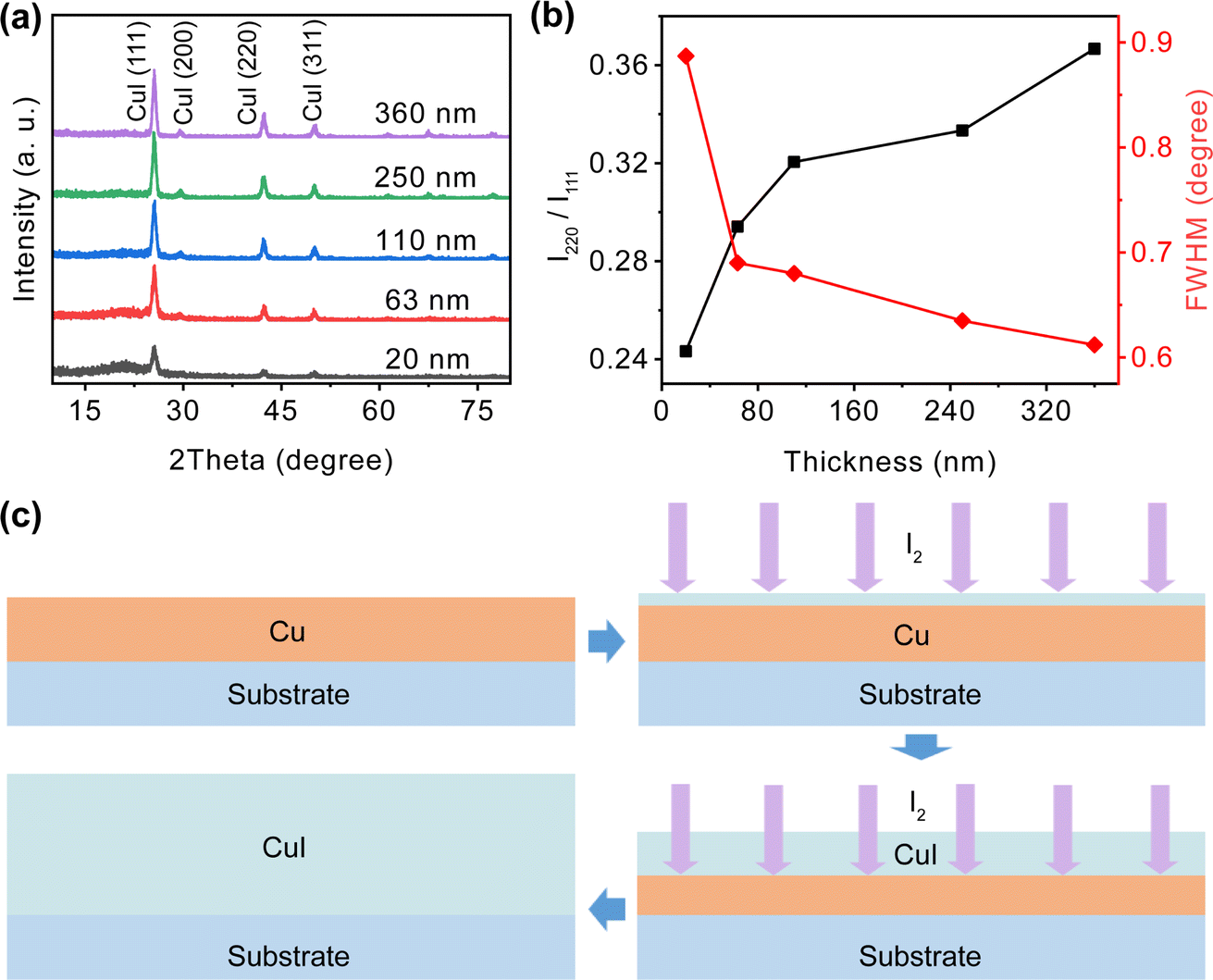 | ||
| Fig. 1 (a) Comparative GIXRD patterns, (b) ratio of (220) and (111) peak intensity (I220/I111), and FWHM value of CuI films as a function of film thickness, (c) schematic diagram of CuI film growth. | ||
In order to study the surface composition with different thickness, we performed XPS measurements on the films, the results are shown in Fig. 2. The peaks at 932 and 952 eV correspond to Cu 2p3/2 and Cu 2p1/2 states of Cu+,50 as shown in Fig. 2(a). In the binding energy ranging from 940 to 945 eV, no Cu2+ species were detected.51 In Fig. 2(b), the peaks at 619 and 631 eV associate with I 3d5/2 and I 3d3/2 states.17 These results indicate that the films are composed of the elements Cu and I, and in combination with the GIXRD patterns in Fig. 1, it can be determined that the crystalline phase of the films is indeed γ-CuI. All the peaks in the XPS spectra are shifted towards small binding energy with increasing film thickness, indicating a gradual decrease in the iodine content of the films.52
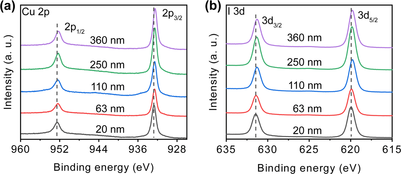 | ||
| Fig. 2 X-ray photoelectron spectroscopy showing the (a) Cu 2p, (b) I 3d spectra of CuI films with different thickness. | ||
The variation in film morphology with thickness was investigated, as shown in Fig. 3(a)–(e). The film with a thickness of 20 nm appears sparse and exhibits noticeable discontinuous voids. In contrast, films with thicknesses of 63 nm, 110 nm, 250 nm, and 360 nm are denser and more continuous. As the film thickness increases, there is a gradual enlargement in grain size. This phenomenon is attributed to the higher abundance of Cu elements in thicker films, allowing for the formation of more CuI nuclei and subsequent merging growth. The surface flatness of the film decreases with increasing film thickness, as shown in Fig. 3(f)–(j). The film roughness values for thicknesses of 20 nm, 63 nm, 110 nm, 250 nm, and 360 nm are 11.9, 8.5, 9.3, 15.1, and 18.4 nm, respectively. The film with a thickness of 20 nm exhibits greater roughness compared to the film with a thickness of 63 nm due to the presence of discontinuous regions and exposed substrate. However, as the film thickness surpasses 63 nm, the surface roughness increases due to the coarsening of the grains. The thickness of the films was measured using a profilometer. In order to determine the growth rate of the films, Cu film with a sputtering time of 60 s was initially prepared, resulting in a measured thickness of 90 nm after iodination. The growth rate of the film was calculated to be 1.5 nm s−1. To grow films with theoretical thicknesses of 20, 60, 100, 200, and 300 nm, the sputtering time was set to 14, 40, 67, 134, and 200 s, respectively. However, the measured thicknesses were 20 nm, 63 nm, 110 nm, 250 nm, and 360 nm. The measured thicknesses of films with sputtering times of 134 s and 200 s were significantly higher than the theoretical thicknesses. This is due to the larger grains present in thicker films, resulting in larger voids between grains, which reduces the density of the films and leads to measured thicknesses exceeding the theoretical values.
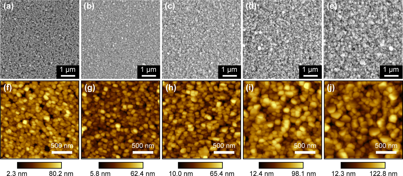 | ||
| Fig. 3 SEM and AFM images of CuI films with thickness of (a and f) 20 nm, (b and g) 63 nm, (c and h) 110 nm, (d and i) 250 nm and (e and j) 360 nm. | ||
The influence of film thickness on the transmittance of the CuI films is presented in Fig. 4(a). Visible light transmittance decreases from 90% to 70% with the increase in film thickness. The enlargement of grain size and film roughness contributes to increased light absorption and surface scattering, resulting in decreased transmittance.40 The fluctuations in the visible light transmission curve for films with thicknesses ranging from 110 nm to 360 nm may arise from interference effects between the film surface and air, as well as between the film and the substrate, attributed to changes in film thickness.53 The optical bandgap of CuI films with varying thickness is depicted based on the Tauc plot method,54 as shown in Fig. 4(b). The optical bandgap of the films decreases as the film thickness rises, possibly attributed to the higher defect density and residual stress in thicker films.55,56
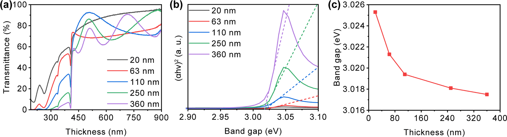 | ||
| Fig. 4 (a) Optical transmission spectra, (b) Tauc plot, (c) optical bandgap of CuI films with different thickness. | ||
The photoluminescence spectra of CuI films with varying thickness are shown in Fig. 5(a). The emission peak at 410 nm is interband transition, while the emission peaks at 420 nm and 720 nm are related to Cu vacancies and I vacancies,57 respectively. As the film thickness increases, the emission peak at 410 nm gradually shifts to 420 nm, indicating an elevation in the concentration of Cu vacancies. The emission intensity at 720 nm increases with the rise in film thickness, indicating a proportional increase in I vacancy concentration with greater film thickness. To achieve a more precise comprehension of the relative concentrations of Cu and I vacancies, we calculated the ratio of the emission intensity at 720 nm to that at 420 nm, denoted as II-v/ICu-v, as shown in Fig. 5(b). The II-v/ICu-v ratio gradually increases with film thickness, indicating a gradual rise in the relative concentration of I vacancies. In general, vacancies accumulation decreases with decreasing grain size.58 In films with small grain size and high grain boundary density, the inadequate growth of grains implies that grain boundary migration is limited. Conversely, in films with large grains, during the grain growth process, grain boundary migration is more extensive, contributing to the formation of vacancies and radiation centers.59,60 Consequently, thinner films exhibit a lower concentration of Cu and I vacancies.
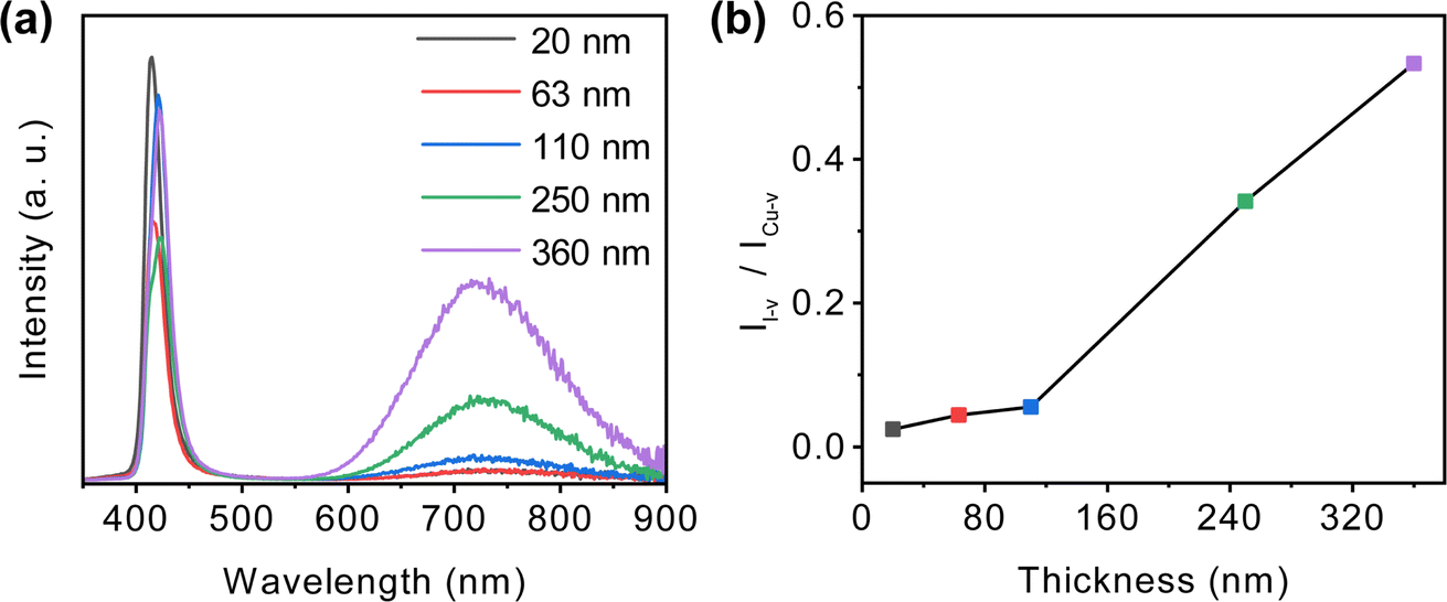 | ||
| Fig. 5 (a) Photoluminescence spectra, (b) peak intensity ratio for I vacancy (I-v) and Cu vacancy (Cu-v) of CuI films with different thickness. | ||
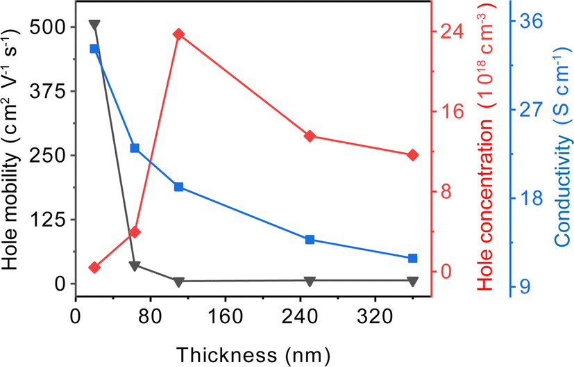
We employed Hall effect measurements to characterize the electrical properties of CuI films with varying thicknesses, as shown in Fig. 6. As the film thickness increases from 20 nm to 110 nm, the hole concentration gradually increases from 4.09 × 10¹⁷ to 2.37 × 1019 cm−3. The increase in hole concentration aligns with the shift of the emission peak from 410 nm to 420 nm, as observed in the Fig. 5(a), substantiating that the concentration of Cu vacancies influences the hole concentration. However, after the film thickness exceeds 110 nm, the hole concentration gradually decreases. I vacancies exert a highly unfavorable influence on hole transport, functioning as trap states that diminish hole concentration and mobility.40 With the thickness of the films on the rise, the concentration of I vacancies increases, leading to a gradual reduction in hole mobility from 506.50 to 6.37 cm2 V−1 s−1. Therefore, the conductivity of the films exhibits a decrease from 33.19 to 11.89 S cm−1 with increasing thickness. The inter-grain spacing increases with the rise in film thickness, also hindering hole transport and resulting in a reduction in conductivity.
 | ||
| Fig. 6 Electrical properties of CuI films as a function of film thickness. | ||
The extent of grain boundary migration can influence the concentration of vacancy defects in CuI films. In films with large grains, grain boundary migration is more extensive during the film growth process, contributing to the formation of vacancies. Regulating the concentrations of Cu and I vacancies enables control over both hole concentration and mobility in CuI films. Cu vacancies are widely acknowledged as the source of p-type conductivity in CuI films, as their concentration determines the hole concentration within the films.24 On the other hand, I vacancies act as trap states, capturing or scattering holes, leading to a decrease in both hole concentration and mobility, thereby deteriorating the conductivity of CuI films.61 Fig. 5 indicated an enhancement in emission peak intensity related to Cu and I vacancies with increasing film thickness, with the ratio of I vacancies peak intensity to Cu vacancies peak intensity gradually increasing. This suggests that thicker films contain higher concentrations of Cu and I vacancies, with a relatively higher concentration of I vacancies. These are attributed to increased grain boundary migration during film growth, leading to the accumulation of vacancies in thicker films. Hall effect measurements in Fig. 6 revealed a gradual decrease in hole mobility and conductivity with increasing film thickness, with an initial increase followed by a decrease in hole concentration. As film thickness increased, the concentration of Cu vacancies rose, consequently resulting in an elevation of the hole concentration. However, I vacancies also increased significantly, acting as trap states to capture holes, resulting in a decrease in hole concentration beyond a film thickness of 110 nm. The increase in I vacancies led to reduced hole mobility, thereby diminishing film conductivity. Thus, controlling the migration of grain boundaries can regulate the concentrations of Cu and I vacancies, thereby enabling control over both hole concentration and mobility.
Currently, there is no acceptable explanation for the correlation between film thickness and hole transport in CuI films. In 2016, Guochen Lin et al. observed, through photoluminescence spectroscopy, a decrease in the concentration of Cu vacancies and an increase in the concentration of I vacancies for CuI films with thicknesses exceeding 80 nm.62 However, they did not elucidate the reasons for the change in vacancy concentration, nor did they investigate the effect of thickness on hole transport. In 2019, Anil Annadi et al. discovered that as the film thickness decreased from 300 nm to 25 nm, the hole concentration in CuI films gradually increased. However, when the thickness was reduced to less than 25 nm, the hole concentration dropped by two orders of magnitude, reaching 9.6 × 1017 cm−3. They hypothesized that the hole concentration in CuI grains remained constant at in the order of 1019 cm−3 across samples of different thicknesses, and interpreted the variation in hole concentration with thickness as Cu vacancies being more prone to form on the (111) crystal plane.53 In 2020, Wei Peng et al. discovered that as the thickness of CuI films increased from 50 nm to 420 nm, the film roughness increased, while the transmittance and optical bandgap decreased. The film conductivity and hole concentration initially increased with film thickness and reached their peak at the thickness of 100 nm, then decreased. The hole mobility increased with increasing film thickness. However, there was no corroborating data derived from photoluminescence spectroscopy, nor was there an explanation for the variation in hole transport with film thickness.49 In 2021, Mokurala Krishnaiah et al. discussed the influence of thickness on the optical detection performance of CuI films but did not investigate the impact of thickness on hole transport.52 In 2021, Beibei Shi et al. observed an increase in peak intensity at 424 nm in the photoluminescence spectrum with increasing thickness, attributing it to the increased presence of excess iodine in CuI films. However, they did not discuss the effect of thickness on hole transport.63 In summary, there is no convincing explanation for the effect of film thickness on hole transport in CuI films. However, the principle proposed in this study, which inhibits grain boundary migration during film growth to reduce the probability of Cu and I vacancies formation, thereby lowering the hole concentration and enhancing hole mobility, holds significant importance for understanding hole transport in CuI films. It also provides guidance for CuI film growth strategy and device applications.
4. Conclusions
P-type transparent conducting CuI films with excellent performance were fabricated through iodination of sputtered Cu precursor films at room temperature. Modulating the film thickness allows control over CuI grain boundary migration, consequently regulating the defect concentration in the films. Thinner films exhibit reduced concentrations of Cu and I vacancies, resulting in decreased hole concentration, improved hole mobility, and enhanced conductivity. The film with a thickness of 20 nm shows the best performance, with a transmittance of 90%, hole concentration of 4.09 × 1017 cm−3, hole mobility of 506.50 cm2 V−1 s−1, and conductivity of 33.19 S cm−1. During the film growth process, thinner films demonstrate limited grain boundary migration, reducing the probability of Cu and I vacancies formation, resulting in lower concentrations of Cu and I vacancies. The reduced Cu vacancies decrease the hole concentration, while the reduced I vacancies enhance the hole mobility and conductivity. The film displays discontinuous regions at a thickness of 20 nm, these discontinuities reduce the hole transport pathway, which is unfavorable for hole transport. However, it exhibits the lowest concentration of I vacancies, thereby significantly enhancing hole mobility, offsetting the adverse effects on hole transport caused by discontinuous regions. In this study, the proposed principle of inhibiting grain boundary migration to reduce the probability of Cu and I vacancies formation, thereby lowering the hole concentration and enhancing hole mobility, provides insightful implications for the application of CuI films in transparent electronics.Author contributions
Ruibin Xue: conceptualization, investigation, methodology, writing – original draft. Gang Gao: supervision, writing – review & editing. Lei Yang: investigation. Liangge Xu: investigation. Yumin Zhang: supervision. Jiaqi Zhu: supervision.Conflicts of interest
There are no conflicts to declare.Acknowledgements
This work is supported by the following grants: the Key Program of National Natural Science Foundation of China (Grant No. 52032004), the National Youth Science Funds of China (Grant No. 52302172). The authors also want to thank Dr Lei Yang from Center of Analysis Measurement of Harbin Institute of Technology, who provided the help about the XPS testing and analysis.References
- Y. Magari, T. Kataoka, W. Yeh and M. Furuta, Nat. Commun., 2022, 13, 1078 CrossRef CAS PubMed.
- H. Hosono, Nat. Electron., 2018, 1, 428 CrossRef.
- E. Fortunato, V. Figueiredo, P. Barquinha, E. Elamurugu, R. Barros, G. Goncalves, S. H. K. Park, C. S. Hwang and R. Martins, Appl. Phys. Lett., 2010, 96, 3 Search PubMed.
- A. Liu, G. X. Liu, H. H. Zhu, B. Shin, E. Fortunato, R. Martins and F. K. Shan, Appl. Phys. Lett., 2016, 108, 233506 CrossRef.
- Y. Ogo, H. Hiramatsu, K. Nomura, H. Yanagi, T. Kamiya, M. Hirano and H. Hosono, Appl. Phys. Lett., 2008, 93, 032113 CrossRef.
- A. Liu, H. Zhu, W. T. Park, S. J. Kang, Y. Xu, M. G. Kim and Y. Y. Noh, Adv. Mater., 2018, e1802379 CrossRef.
- D. C. Look, K. D. Leedy, L. Vines, B. G. Svensson, A. Zubiaga, F. Tuomisto, D. R. Doutt and L. J. Brillson, Phys. Rev. B: Condens. Matter Mater. Phys., 2011, 84, 115202 CrossRef.
- M. Snure and A. Tiwari, Appl. Phys. Lett., 2007, 91, 092123 CrossRef.
- H. Kawazoe, M. Yasukawa, H. Hyodo, M. Kurita, H. Yanagi and H. Hosono, Nature, 1997, 389, 939–942 CrossRef CAS.
- S. Jeong, S. Seo and H. Shin, RSC Adv., 2018, 8, 27956–27962 RSC.
- K. Ueda, T. Hase, H. Yanagi, H. Kawazoe, H. Hosono, H. Ohta, M. Orita and M. Hirano, J. Appl. Phys., 2001, 89, 1790–1793 CrossRef CAS.
- B. J. Ingram, B. J. Harder, N. W. Hrabe and T. O. Mason, Chem. Mater., 2004, 16, 5623–5629 CrossRef CAS.
- H. Yanagi, T. Hase, S. Ibuki, K. Ueda and H. Hosono, Appl. Phys. Lett., 2001, 78, 1583–1585 CrossRef CAS.
- A. Kudo, H. Yanagi, H. Hosono and H. Kawazoe, Appl. Phys. Lett., 1998, 73, 220–222 CrossRef CAS.
- K. Ueda, K. Takafuji, H. Hiramatsu, H. Ohta, T. Kamiya, M. Hirano and H. Hosono, Chem. Mater., 2003, 15, 3692–3695 CrossRef CAS.
- G. Gao, K. Li, L. Yang, F. Xia, L. Xu, J. Han, H. Gong and J. Zhu, Mater. Today Phys., 2023, 35, 101089 CrossRef CAS.
- N. Yamada, R. Ino and Y. Ninomiya, Chem. Mater., 2016, 28, 4971–4981 CrossRef CAS.
- R. Nagarajan, A. D. Draeseke, A. W. Sleight and J. Tate, J. Appl. Phys., 2001, 89, 8022–8025 CrossRef CAS.
- K. H. L. Zhang, Y. G. Du, A. Papadogianni, O. Bierwagen, S. Sallis, L. F. J. Piper, M. E. Bowden, V. Shutthanandan, P. V. Sushko and S. A. Chambers, Adv. Mater., 2015, 27, 5191–5195 CrossRef CAS PubMed.
- C. Yang, M. Kneibeta, M. Lorenz and M. Grundmann, Proc. Natl. Acad. Sci. U. S. A., 2016, 113, 12929–12933 CrossRef CAS PubMed.
- A. Liu, H. H. Zhu, M. G. Kim, J. Kim and Y. Y. Noh, Adv. Sci., 2021, 8, 2100546 CrossRef CAS PubMed.
- D. Huang, Y. J. Zhao, S. Li, C. S. Li, J. J. Nie, X. H. Cai and C. M. Yao, J. Phys. D: Appl. Phys., 2012, 45, 145102 CrossRef.
- H. Chen, C. Y. Wang, J. T. Wang, Y. Wu and S. X. Zhou, Phys. B, 2013, 413, 116–119 CrossRef CAS.
- N. Yamada, R. Ino and Y. Ninomiya, Chem. Mater., 2016, 28, 4971–4981 CrossRef CAS.
- M. Grundmann, F. L. Schein, M. Lorenz, T. Bontgen, J. Lenzner and H. von Wenckstern, Phys. Status Solidi A, 2013, 210, 1671–1703 CrossRef CAS.
- Z. Zhang, M. Zhao, C. L. Hu, L. Xiong, X. Y. Zhu, T. Y. Zhai and W. X. Liang, J. Phys. Chem. C, 2022, 126, 20920–20928 CrossRef CAS.
- K. X. Zhang, S. W. Wang and L. X. Yi, Opt. Mater., 2022, 134, 113204 CrossRef CAS.
- S. Koyasu and M. Miyauchi, J. Electron. Mater., 2020, 49, 907–909 CrossRef CAS.
- A. Liu, H. H. Zhu, W. T. Park, S. J. Kang, Y. Xu, M. G. Kim and Y. Y. Noh, Adv. Mater., 2018, 30, 1802379 CrossRef.
- A. Liu, H. H. Zhu, W. T. Park, S. J. Kim, H. Kim, M. G. Kim and Y. Y. Noh, Nat. Commun., 2020, 11, 4309 CrossRef CAS PubMed.
- C. Yang, D. Souchay, M. Kneiss, M. Bogner, M. Wei, M. Lorenz, O. Oeckler, G. Benstetter, Y. Q. Fu and M. Grundmann, Nat. Commun., 2017, 8, 16076 CrossRef CAS.
- P. Darnige, Y. Thimont, L. Presmanes and A. Barnabe, J. Mater. Chem. C, 2023, 11, 630–644 RSC.
- M. M. Byranvand, T. Kim, S. Song, G. Kang, S. U. Ryu and T. Park, Adv. Energy Mater., 2018, 8, 1702235 CrossRef.
- H. X. Wang, Z. Yu, J. B. Lai, X. K. Song, X. C. Yang, A. Hagfeldt and L. C. Sun, J. Mater. Chem. A, 2018, 6, 21435–21444 RSC.
- Y. Z. Liu, T. Zhang, L. Y. Shen, H. S. Wu, N. Wang, F. Z. Wang, X. H. Pan and Z. Z. Ye, ACS Appl. Mater. Interfaces, 2023, 15, 29267–29277 CrossRef CAS PubMed.
- G. J. Xiang, J. M. Zhang, Z. Yue, X. Zhang, C. L. Song, B. X. Ding, L. K. Wang, Y. Wang, H. Y. He, H. Wang and Y. Zhao, Appl. Surf. Sci., 2023, 640, 158397 CrossRef CAS.
- C. Yang, M. Kneiss, M. Lorenz and M. Grundmann, Proc. Natl. Acad. Sci. U. S. A., 2016, 113, 12929–12933 CrossRef CAS.
- D. K. Kaushik, M. Selvaraj, S. Ramu and A. Subrahmanyam, Sol. Energy Mater. Sol. Cells, 2017, 165, 52–58 CrossRef CAS.
- P. Storm, K. Karimova, M. S. Bar, S. Selle, H. von Wenckstern, M. Grundmann and M. Lorenz, ACS Appl. Mater. Interfaces, 2022, 14, 12350–12358 CrossRef CAS PubMed.
- V. Raj, T. Lu, M. Lockrey, R. Liu, F. Kremer, L. Li, Y. Liu, H. H. Tan and C. Jagadish, ACS Appl. Mater. Interfaces, 2019, 11, 24254–24263 CrossRef CAS.
- S. L. Dhere, S. S. Latthe, C. Kappenstein, S. K. Mukherjee and A. V. Rao, Appl. Surf. Sci., 2010, 256, 3967–3971 CrossRef CAS.
- S. Inudo, M. Miyake and T. Hirato, Phys. Status Solidi A, 2013, 210, 2395–2398 CrossRef CAS.
- M. Tsuji, S. Iimura, J. Kim and H. Hosono, ACS Appl. Mater. Interfaces, 2022, 14, 33463–33471 CrossRef CAS.
- T. Jun, J. Kim, M. Sasase and H. Hosono, Adv. Mater., 2018, 30, 1706573 CrossRef PubMed.
- R. Xue, G. Gao, L. Yang, L. Xu, Y. Zhang, J. Zhu and R. Xue, J. Mater. Chem. C, 2023, 11, 13681–13690 RSC.
- A. Yan, C. Wang, J. Yan, Z. Wang, E. Zhang, Y. Dong, Z. Y. Yan, T. Lu, T. Cui, D. Li, P. Shen, Y. Jin, H. Liu, Y. Yang and T. L. Ren, Adv. Funct. Mater., 2023, 34, 2304409 CrossRef.
- X. Zhang, Q. Liao, S. Liu, Z. Kang, Z. Zhang, J. Du, F. Li, S. Zhang, J. Xiao, B. Liu, Y. Ou, X. Liu, L. Gu and Y. Zhang, Nat. Commun., 2017, 8, 15881 CrossRef CAS PubMed.
- S. Lei, X. Wang, B. Li, J. Kang, Y. He, A. George, L. Ge, Y. Gong, P. Dong, Z. Jin, G. Brunetto, W. Chen, Z.-T. Lin, R. Baines, D. S. Galvão, J. Lou, E. Barrera, K. Banerjee, R. Vajtai and P. Ajayan, Nat. Nanotechnol., 2016, 11, 465–471 CrossRef CAS.
- W. Peng, L. X. Li, S. H. Yu, H. R. Zheng and P. Yang, Appl. Surf. Sci., 2020, 502, 144424 CrossRef CAS.
- I. Platzman, R. Brener, H. Haick and R. Tannenbaum, J. Phys. Chem. C, 2008, 112, 1101–1108 CrossRef CAS.
- M. C. Biesinger, Surf. Interface Anal., 2017, 49, 1325–1334 CrossRef CAS.
- M. Krishnaiah, A. Kumar, A. K. Kushwaha, J. Song and S. H. Jin, Mater. Lett., 2021, 305, 130815 CrossRef CAS.
- A. Annadi, N. D. Zhang, D. B. K. Lim and H. Gong, ACS Appl. Electron. Mater., 2019, 1, 1029–1037 CrossRef CAS.
- J. Tauc and A. Menth, J. Non-Cryst. Solids, 1972, 8–10, 569–585 CrossRef CAS.
- P. Tyagi and A. G. Vedeshwar, Phys. Rev. B: Condens. Matter Mater. Phys., 2001, 64, 245406 CrossRef.
- R. Sathyamoorthy and S. Senthilarasu, Sol. Energy, 2006, 80, 201–208 CrossRef CAS.
- K. X. Zhang, S. W. Wang, L. Y. Bai, Y. Wang, K. Ou, Y. W. Zhang and L. X. Yi, J. Lumin., 2019, 214, 116522 CrossRef CAS.
- Y. Yang, H. C. Huang and S. J. Zinkle, J. Nucl. Mater., 2010, 405, 261–265 CrossRef CAS.
- M. Upmanyu, D. J. Srolovitz, L. S. Shvindlerman and G. Gottstein, Interface Sci., 1998, 6, 287–298 CAS.
- P. Ballo, J. Degmová and V. Slugeň, Phys. Rev. B: Condens. Matter Mater. Phys., 2005, 72, 064118 CrossRef.
- D. H. Kim, S. B. Cho, C. X. Li and I. Park, Thin Solid Films, 2023, 782, 140029 CrossRef CAS.
- G. C. Lin, F. Z. Zhao, Y. Zhao, D. Y. Zhang, L. X. Yang, X. O. Xue, X. H. Wang, C. Qu, Q. S. Li and L. C. Zhang, Materials, 2016, 9, 990 CrossRef PubMed.
- B. B. Shi, J. B. Jia, X. Feng, G. C. Ma, Y. Q. Wu and B. Q. Cao, Vacuum, 2021, 187, 110076 CrossRef CAS.
| This journal is © The Royal Society of Chemistry 2024 |