
 Open Access Article
 This Open Access Article is licensed under a Creative Commons Attribution-Non Commercial 3.0 Unported Licence
Structural and morphological investigation of (R)-α-phenylethylammonium-oxalate in bulk vs. nanowires on a modified substrate surface†
Sanja Burazer *ab,
Tereza Košutováb,
Lukáš Horákb,
Milan Dopitab,
Ana Šantića and
Anna Fučíkováb
*ab,
Tereza Košutováb,
Lukáš Horákb,
Milan Dopitab,
Ana Šantića and
Anna Fučíkováb
aRuđer Bošković Institute, Bijenička cesta 54, 10000 Zagreb, Croatia. E-mail: Sanja.Burazer@irb.hr
bFaculty of Mathematics and Physics, Charles University, Ke Karlovu 3, 12000 Prague, Czech Republic
First published on 12th March 2024
Abstract
A chiral organic insulator, (R)-α-phenylethylammonium-oxalate (RAPEAO), was prepared in the forms of single-crystal, powder and spin-coated layers on silicon substrate surfaces modified by plasma treatment or a (3-aminopropyl)triethoxysilane (APTES) polymer layer. For spin-coated samples, different deposition conditions have been investigated – various thicknesses controlled by speed and the number of repeated cycles, deposited continuously or by a layer-by-layer technique. The chemistry of this compound did not allow the deposition of the continuous thin film, yet, it caused the formation of a few nuclei on the substrate surface. Modification of the substrate with low temperature plasma caused the increased number of nuclei as well as enabled the growth of the nanowires, which was confirmed by atomic force microscopy (AFM) images. The same effect has been observed from the X-ray diffraction (XRD) measurements, where preferential growth of the studied compound in one direction was confirmed by grazing incidence, as well as wide reciprocal space mapping (WRSM). XRD studies confirmed the structural similarity of the compound, disregarding the compound form ranging from nanowires on the substrate to the bulk. Finally, the substrate covered by APTES thin film has had increased coverage of the substrate surface by the studied compound. Impedance spectroscopy revealed that the electrical conductivity of the sample in bulk at 20 °C is 6.3 × 10⁻¹⁵ (Ω cm)−1, indicating the insulating properties of the material.
Introduction
It is well-known that the same compound in the shape of a thin film and bulk can exhibit differences. When going from bulk to the nano regime, the surface to volume ratio of the material becomes high, which is one of the main causes of alteration of the numerous physical as well as chemical properties. From a gas sensing point of view, the high-textured thin film is more suitable towards the selectivity of the particular gas in a mixture of several gases. Moreover, the high surface area of the thin film provides more active sites for the adsorption of analyte gas molecules. Differences between bulk and thin films can also be observed in atomic diffusion and chemical reactivity, stress, degradation and wear; nucleation growth and grain size, effects on the interfaces of the film or film/substrate and different properties.1Deposition of the layer implies processing above the substrate surface, by chemical or physical vapour deposition, sputtering, thermal evaporation or spin coating. Spin coating is a simple, relatively inexpensive, method of centrifugal deposition of the solution on a substrate that is fixed to a plate by an aspirator. After spinning the plate, centrifugal force spreads material uniformly across the whole substrate surface. The material is quickly dried during the rotation process or by additional evaporation during steaming of the sample. Acceleration and speed of rotation control the thickness of the layer. This method is quick, and the loss of material is not as much as it is in vapor-phase deposition, but it has the drawback of keeping the contaminants, such as traces of solvents, inside the film. Additionally, homogeneity and roughness, as well as the formation of extra thin films are still quite challenging.2–4 By changing the number of cycles, as well as the speed of rotation in the spin coating process, the thickness of the film is changing, as well as the properties of the deposited material. Li and co-authors reported how concentration and spin speed during the deposition affect the optical and electrical properties of silver nanowire transparent electrodes. Their results showed that the distribution of silver nanowires on the substrate increased the density with increasing solution concentration and the decrease in spin speed.5 Na and co-authors revealed that lamellar stacking and π–π stacking interactions in the most widely studied semiconducting polymer, poly(3-hexylthiophene) (P3HT) thin films were enhanced due to the slow growth process caused by the remaining solvent following a short spin-coating period. This process allows for the creation of polymer thin films that are highly crystalline, homogenous, and reproducible without the need for any additional treatments. Additionally, they showed how volume, boiling point, and dissolving power of the solvents introduced significantly impacted both the solidification process of the P3HT film and the electrical properties of the resulting P3HT films.4
Nanostructured thin films are important in numerous fields of modern technology and science because of a strong correlation between their chemical and physical properties, such as electronic, optical or mechanical properties, and their structural features of the material, such as crystallinity, size and shape.6–9 Thus, film structural properties are crucial to the stability and functionality of thin films.10 X-ray measurement techniques are most often used for the structural characterization of various thin-film materials and devices. However, due to the characteristics of thin films, such as strong preferred orientation, which limits the detection to only one set of specific lattice planes, measurements of thin films are more complicated than powder samples. An essential feature of X-ray methods in the characterization of thin films is the possibility of modifying the analysis depth by changing the incident angle onto the surface and characterizing the buried interface structure. Compared with 2θ/θ scan of a powder sample, where one can get only the information from lattice planes parallel to the sample surface, with thin films, it is necessary to pay attention to the orientations of the lattice planes and the direction of the X-ray beam, which impinges onto the sample. This information is often insufficient for the epitaxial thin film or any strongly preferred-oriented thin film, and lattice planes inclined to the sample's surface, such as reciprocal space maps, should be measured.11
Through the morphological studies of thin films, the idea about the growth mechanism arises, this understanding is crucial for the fabrication of nanostructured materials in a controlled way for creating nanomaterial with desired properties.12–15 It is not always easy to produce epitaxial thin film, however different formations are possible, such as bound nanoparticles, nanoclusters or nanowires. Nanoparticles can be used in many fields of research and technology; from catalysis, cancer therapy and diagnosis to water purification and other biological and environmental applications.16–20 With different morphology of the deposited layer, different results can be expected depending on the formed shape. As an example, Broitman and co-authors used quartz crystal microbalance placed in a vacuum chamber to quantify the amount and kinetics of water adsorption onto the samples and results showed that nanowire samples, which have higher surface areas than the thin films, adsorb significantly more water. ZnO structure is of the same, wurtzite type, both in nanowires and thin films.21,22
Atomic force microscopy (AFM), as one of the most popular scanning probe microscopy methods, enables imaging topography of almost any type of surface, such as polymers, ceramics, and composites. The substrate surface greatly affects the analysis of the sample, therefore, deposition on a very rough substrate disables the straightforward small particle size analysis. Additionally, nanoparticle agglomeration and self-ordering also influence the analysis of obtained AFM data. Intermittent contact mode was used in this work, where the AFM cantilever is vibrating above the sample surface so that the tip is in contact with the surface only intermittently in the tapping mode. This mode helps to reduce wearing off the cantilever and therefore obtain as sharp image as possible during the whole measurement, also we do not damage the studied samples because the contact with them is minimal. As a result, the AFM gives a surface topography profile.23 By AFM, it is possible to analyse nanoparticles on rough substrates or those that are not isolated, but for this purpose, it is necessary to use a simple particle deposition modelling technique, together with a tip-sample convolution algorithm, and then one can get relatively easily estimation of uncertainty components related to data processing methods in nanoparticle analysis.24
Treatment of the substrate by polymers can improve the coverage of the substrate surface by deposited studied material but also can change the properties of the deposited material. Author's previous paper investigated differences in the electrochemical properties of the PbO2 deposited on the bare gold electrode and PbO2 deposited on the gold electrode covered with polymer Nafion®. Results showed that there was no structural change of deposited PbO2 with or without polymer, but electrochemical behaviour was drastically different. Nafion® layer showed a favourable effect on the efficiency of the deposition process which was caused by both thermodynamic and kinetic reasons. At Nafion® covered gold electrode, electrodeposition process goes via Pb(III) intermediate species which are stabilized within Nafion® membrane.25
Transition towards a metal-free materials for different applications – from transistors, sensors to whole field of batteries is highly represented in the research.26,27 Nowadays, electroactive organic materials present a promising alternative to inorganic electrode materials for the new generation of green Li-ion batteries. This is enabled by their sustainability, environmental benignity, and low cost. A great example of organic nanowires application as electrodes is presented in the work of Luo and collaborators where they have synthesized and used croconic acid disodium salt (CADS) wires with diameters from 150 nm to 10 μm by facile antisolvent crystallization method. Those wires with a smaller diameter and larger surface area were of higher capacity, longer cycle life and excellent rate capability. Additionally, the authors managed to retain the initial capacity after 110 deep charge/discharge cycles.28 The work of Watanabe and co-authors showed that graphite-based carbon electrodes may be applied and designed directly on an organic single-crystalline thin film via electrostatic spray coating, forming completely organic thin-film transistor (OTFT), a promising building blocks of flexible printable electronic devices, constructed entirely from carbon-based materials.29,30 Organic conductor, bis(ethylenedithio)tetraselenafulvalene have been explored as a part of topological insulators.31 A distinct type of organic semiconductors that serve as a versatile foundation for electrical, spintronic, and energy-harvesting devices show dependence of structural modifications, particularly in terms of electrical, optical, and dielectric properties.32 Very popular application of organics is as an insulators. Insulators in semiconductors have two main functions: providing electrical insulation between metallization levels and passivating the semiconductor structure electrically, chemically, and mechanically. During the initial phase of semiconductor development, insulation and passivation were carried out using only inorganic insulators such as frit glass, sputtered SiO2 and Sb2S3, which were deposited using chemical vapor or plasma deposition methods. During the early 1970s, the initial trials to use organic materials for device insulation and passivation were documented. Currently, organic insulators are becoming the cutting-edge standard in the semiconductor industry. Organic insulating materials offer benefits such as cost-effectiveness, easy manufacturing, strong mechanical and electrical insulation properties. They are widely used in transmission and transformation lines across different voltage levels and equipment, contributing significantly to the power grid's safe operation. Chemically, popular in use are polyimides, epoxy resin, polycarbonates and many others.33–39
Multifunctional materials are formed by combining different constituents. As an example, it is possible to introduce proton carriers by adding a counterion like hydronium (H3O+), ammonium [NH4+, (CH3)2NH2+,…], or an anion (SO42−) during synthesis, which leads to the formation of charged compounds. The oxalate anion, C2O42−, plays a crucial role in designing and synthesizing multifunctional materials because of its various coordination choices with metal centers and its ability to influence electrical phenomena. Oxalate-based compounds with consistent structures and robust frameworks typically demonstrate strong water and chemical resistance when exposed to varying levels of humidity and temperature.40–47
Many of the organic compounds have optical activity what was investigated in numerous cases. One of them is research of Boskei and collaborators where salts of eight achiral dicarboxylic acids with a-phenylethylamine are synthesized and analyzed using IR spectroscopy, density measurements, and X-ray crystallography to differentiate between racemic compound and conglomerate formation. Conglomerate formation occurs when protonated and deprotonated carboxylic groups create hydrogen bound chains instead of cyclic intramolecular hydrogen bonds.48
Motivated by the above-referenced examples, amine and oxalate group properties, we investigated the structure and the properties of RAPEAO, material formed from amine and oxalic acid, reported as a chirally pure material in the research of Kozma and collaborators.48–51 The same group investigated optical properties and crystal structures of those optically active racemic forms. The crystal structures of (R)-α-phenylethylammonium oxalate [C2; a = 10.786(1), b = 7.4300(6), c = 11.4930(7) Å, beta = 98.661(6)°; Z = 4] and (R,S)-α-phenylethylammonium oxalate (Pca2(1); a = 12.237(4), b = 6.786(5), c = 21.859(4) Å; Z = 4) were determined and are compared.49
Optical behaviour of this compound and similar to it has been thoroughly investigated in previous literature. Kozma and co-authors studied the enantiomeric enrichment of a-phenylethylamine enantiomeric mixtures using achiral dicarboxylic acids. Oxalic, malonic, fumaric, and phthalic acids were utilized as achiral agents. The study compared the effectiveness of enantiomeric enrichment via partial salt production followed by distillation with enantiomer separation using crystallization of the neutral salt. It was concluded that enantiomeric separation cannot occur in the absence of a solid phase. RAPEAO shows good solubility in water and poor in ethanol, similar to other oxalic acid salts.48–51
A narrow area of investigated properties together with known information about a compound and chemical constituents of RAPEAO which offer wide application window, gave us the reason to explore and compare the structural characteristics, as well as properties of the same compound in the shape of single-crystal, powder and spin-coated film. Additionally, in order to see the possible differences in morphology, deposition was done on pure silicon substrate surfaces or those modified by plasma treatment or polymer layer and characterized by X-ray techniques, as well as by AFM. To determine the feasibility of incorporating organic substances into electronic devices, the conductivity of the sample was measured by impedance spectroscopy.
Results and discussion
Structural characterization
Synthetic procedures included both slow evaporation crystallization from the solution prepared in glass, and deposition on the substrate by spin-coating technique. In each case, the same compound was formed, which was confirmed by IR spectroscopy and X-ray diffraction measurements. After single crystal diffraction, it was realized that the prepared compound is already known, RAPEAO, that crystallizes in the monoclinic C2 space group deposited in the CSD database, but its properties are unexplored, except optical characteristics, wherefrom was known that this is chirally pure compound. The other enantiomer of it crystallizes in the orthorhombic Pca21 group. The comparison of the structures is shown in Fig. S1.† The purity of the powder sample was confirmed by Rietveld refinement on PXRD data (Fig. 1a).52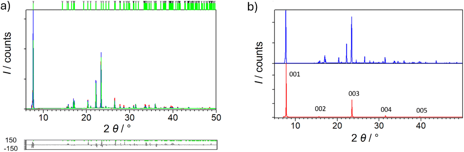 | ||
| Fig. 1 (a) Rietveld refinement52 of sample P1. Experimental data are given in red line, the calculated pattern is shown in blue and difference plot in grey. Green vertical marks show the positions of diffraction lines belonging to monoclinic RAPEAO (C2 space group). (b) Comparison of the PXRD data from sample P1 (blue curve) and BB measurement on the thin film of sample S1 (red curve). | ||
The fact that this compound has never been prepared in the shape of a thin film, nor there is any reported detailed structural analysis, motivated us to compare the structural properties in single-crystal, thin film and powder samples. A similar structural analysis was done for all our samples, prepared under different conditions as described in the Experimental section (samples S1–S4), and there was no difference regarding the structure (Fig. S2†), therefore we are showing/presenting measurements from sample S1.
Since the layer was expected to be very thin and polycrystalline, sample S1 was measured in parallel beam geometry, but no intensity from the layer was observed. Therefore, the sample was remeasured in symmetrical Bragg–Brentano geometry and only 00L peaks were observed. This indicated that there could be a single-crystal epitaxial layer or polycrystalline layer with (001) out-of-plane oriented crystallites (still it could be in-plane oriented similarly to epitaxial one). The comparison of diffractograms of the polycrystalline sample P1 and the spin-coated sample S1 on the substrate is shown in Fig. 1b.
In order to determine the exact orientation of the crystallites, wide reciprocal space maps were measured. For a truly compact epitaxial layer, even the short WRSM measurement in significant azimuthal orientations (determined for the substrate) would show asymmetric Bragg reflections of the layer corresponding to its epitaxial relation, however, this was not the case here. Thus, only two symmetrically non-equivalent azimuths (according to the surface symmetry of the substrate; 0° and 45°) were chosen to be remeasured with significantly longer counting time to suppress the noise in the data (Fig. 2).
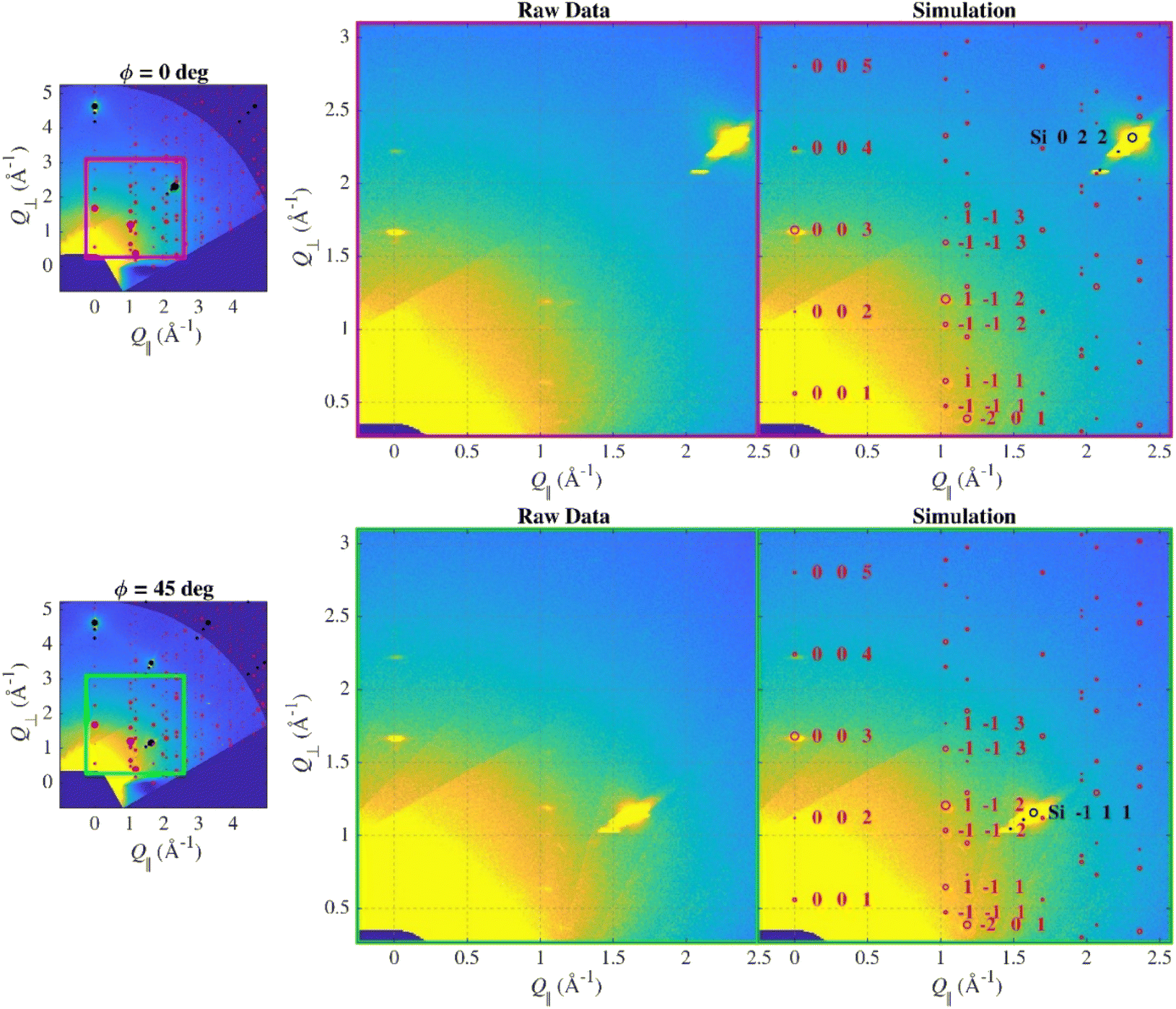 | ||
| Fig. 2 WRSMs for sample S1 measured in two azimuthal directions. Upper maps correspond to the vertical cut in reciprocal space along Si [100], while bottom maps correspond to the cut along Si [−110] direction. Full experimental data (left images) are zoomed to the region where we observe asymmetric Bragg reflections from the crystals on the surface. On the right, both the raw and overlaid experimental data are shown in zoomed regions. The size of the red markers corresponds to the calculated squared structure factors, which roughly correspond to the intensity of the observed spots. | ||
Indeed, several diffraction spots from the layer were observed, their intensity and the positions were identical in both maps indicating that the in-plane orientation of the crystallites is random (fibre texture). The WRSM simulation considering both the expected crystallographic structure and the fibre texture orientations fitted the data well and the simulated and measured intensities are more-less comparable, thus we can tell that the structure of the deposited sample is the same as in the single-crystal.
Due to the fibre texture, there were no lines in PB geometry since the path of the scan in reciprocal space does not lead through any intense spot, but the Bragg–Brentano scan does (Fig. 3).
 | ||
| Fig. 3 Simulated PB (omega = 1.5 deg) (black) and BB (green) paths in WRSM. | ||
Topological characterization
The sample S1 prepared by layer-by-layer deposition was characterized by the AFM technique to determine its topology. Although a very thin film was expected to be on the substrate surface, the AFM measurement showed that instead of a thin film, we synthesized nanowires (Fig. 4). This finding agrees both with reflectivity measurement (Fig. S3†) where no reflection from the layer was observed, meaning that the layer either is not there or it has negligible mean density, and with WRSM measurements (Fig. 2) confirming the fibre texture of the sample. For this molecule, the nanowires occur when growth in one direction is preferred, which causes the fibre texture.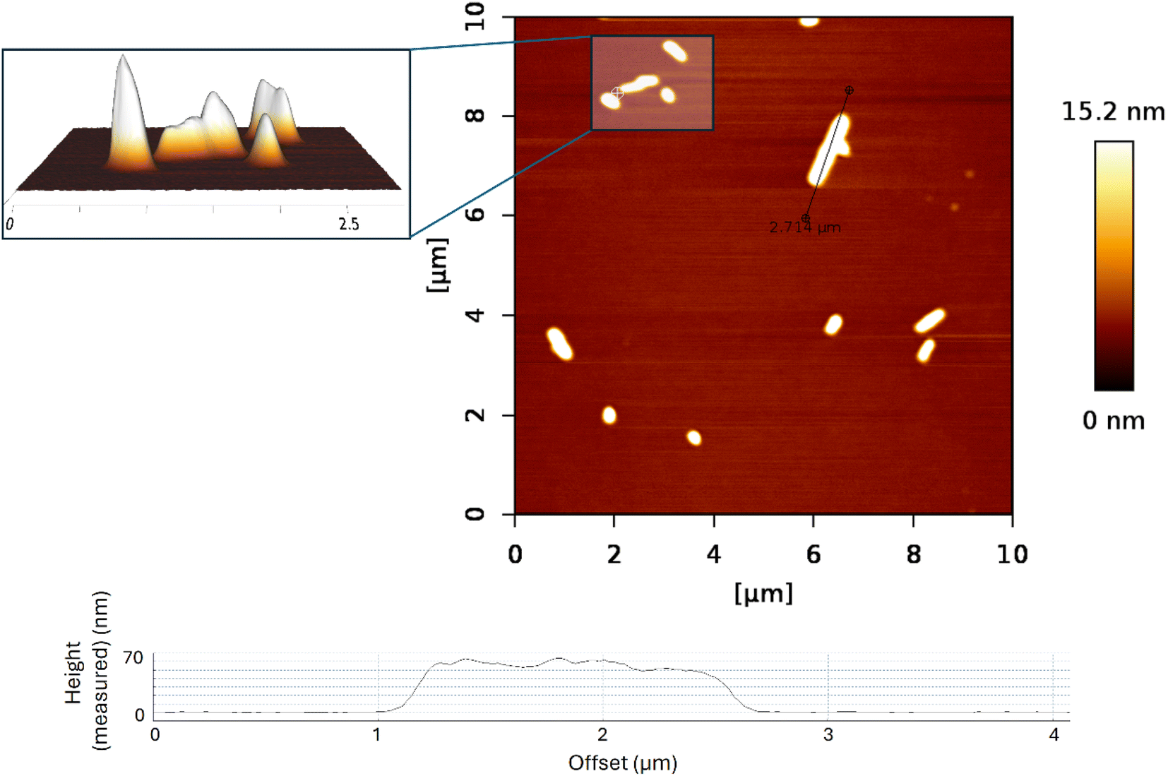 | ||
| Fig. 4 AFM images of sample S1 (RAPEAO on a bare silicon substrate); graphical representation of the measured height of the highest nanopillars. | ||
According to the AFM measurement, the nanowires had a width of 150–300 nm and were 200–3000 nm long when sample deposition was done layer-by-layer. That means that one layer of one reactant solution was deposited, after that substrate was spinned, and above that one layer of another reactant solution was deposited and the substrate was again spinned till the complete drying of the layer. The process is repeated to get a thicker layer. The top of the nanowire is not flat, but the difference in the height on individual nanowires is quite small (around 10 nm for the long ones), the top rather consists of several little hills, this again supports the fact that the layer is grown from inhomogeneities in the wafer, see the inset of Fig. 4.
The height of wires ranged between 10 and 30 nm with the occasional presence of nanopillars which were up to 60 nm in height (Fig. 4). The nanowires have been formed most probably on inhomogeneities on the wafer, which served as starting seeds for the growth of the nanowires.
These observations led us to modify the silicon substrate (Fig. 5) for the next depositions, so more nanowires or optimally a flat layer of the molecule could be grown.
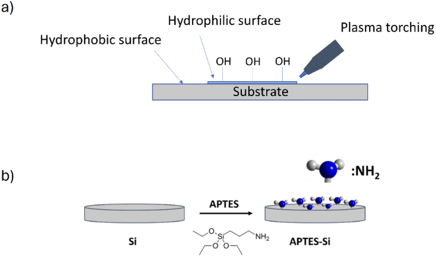 | ||
| Fig. 5 Substrate treatment by (a) plasma torching and (b) APTES polymer. | ||
When the deposition was done from the final solution, by spin coating the RAPEAO solution in methanol prepared in the glass (S2), we got almost no material on the surface, just a few nucleation centres and small nanoparticles growing into height by increasing number of cycles (Fig. 6a). To eliminate these, we treated the substrate with a plasma torch (sample S3). This was done to create more hydrogen bonds on the surface (Fig. 5a) so that amine groups from our molecule could connect to the surface more easily. Despite the increased number of nucleation centres after ozone treatment, there was still no thin film formed on the substrate and we observed just an increased number of particles (Fig. 6b).
 | ||
| Fig. 6 2D and 3D AFM images of samples (a) S2 (RAPEAO on bare silicon substrate) and (b) S3 (RAPEAO on substrate modified by ozone). | ||
Another tested treatment of the substrate was a modification by polymer (sample S4), APTES, that was supposed to enable an increase in the surface coverage by adding amine groups to the surface resulting in easier attachment of our amine on a pure silicon (Fig. 5b).
Although we still did not succeed in the formation of a continuous film, we obtained circular structures with diameters up to 1000 nm, which were quite homogenous in height of 12 nm on average on 4 nm substrate layer. The height homogeneity is disrupted by a few hills that are of the height of 60–120 nm (Fig. 7). These structures show that instead of the nanowire structure we tend to grow planar structures, but still, the covering of the substrate layer is inhomogeneous. The possible cause of this is either inhomogeneities in the APTES covering or more probably the presence of impurities from the starting solutions. If we look closely at individual rings we can see structures resembling flower petals where some of them are quite flat with relatively big area which has holes inside them but otherwise, their size is much bigger than the nanowires presented in this work.
 | ||
| Fig. 7 2D and 3D AFM images of sample S4 (RAPEAO on substrate modified by APTES) showing the circular layer of above mentioned molecules. The ring structures have a much bigger surface area than nanowires. | ||
Thermal characterization and electrical conductivity
From the single-phase powder sample, the thermogravimetric curve was measured. The decomposition started at 40 °C. This low decomposition temperature is caused by the solely organic composition of the compound.Motivated by the popular application of organics in electronic devices, a pellet was used for measuring the conductivity of the sample by impedance spectroscopy. The complex impedance plot of the sample exhibits an arc with high values of impedance indicating very low electrical conductivity, see Fig. 8. The obtained impedance data can be well approximated by the equivalent circuit consisting of a parallel combination of resistor and capacitor. The parameters of the equivalent circuit, i.e. electrical resistance (R) and capacitance (C), obtained by the complex non-linear least squares fitting are given in the legend in Fig. 8. From the value of electrical resistance (R) and electrode dimensions (A is the electrode area and d is the thickness of the pellet), DC conductivity, σDC, was calculated according to the relation: σDC = d/(A × R). The electrical conductivity of the sample at 20 °C is 6.3 × 10⁻¹⁵ (Ω cm)−1 indicating insulating properties of the material, therefore enabling its application in separators in batteries or other small electronic devices.53
 | ||
| Fig. 8 Complex impedance plot of the sample at 20 °C and corresponding equivalent circuit. | ||
Earlier investigated optical characteristics of RAPEAO confirmed its' chiral activity.48–51 From the literature, it is known that organic thin films capable of emitting and absorbing circularly polarized light have been shown to offer potential for significant technological advancements, such as efficient high-performance displays, 3D imaging, and all-organic spintronic devices. Until date, the source of the significant chiroptical effects remained elusive. In the research of Wade and co-authors, it has been confirmed that under conditions relevant for device fabrication – the large chiroptical effects are caused by magneto-electric coupling (natural optical activity), not structural chirality as previously assumed.54 It is also known from the literature that π-stacking results in high mobilities in devices such as transistors, which is reported to be the result of increased overlap between the electronic wave functions of neighbouring molecules in the stack.54,55 Bandwidth increases as the overlap in electronic wavefunction is stronger, which directly correlates to electrical conductivity in the coherent transport regime.56 RAPEAO showed insulating properties of the material that can be corroborated via van der Waals interactions and hydrogen bonds or, in other words, by lack of the π-stacking.57 The visualizations of the crystal structures were made by program VESTA (Fig. 9).58
 | ||
| Fig. 9 RAPEAO structure with van der Waals interactions and hydrogen bonds. Carbon is shown as a brown ball, oxygen as red, nitrogen as blue and hydrogen as pink balls. | ||
Conclusions
The similarity of the (R)-α-phenylethylammonium-oxalate (RAPEAO) crystal structures prepared by different conditions was confirmed by the X-ray diffraction measurements. By spin coating of RAPEAO no epitaxial film was formed, however, by tuning the substrate functionalization, we obtained the circular structures, homogenous in height and more or less forming a layer. Deposited material has in general a polycrystalline nature with a strong preferred orientation, caused by the growth of nanowires, especially on plasma or APTES-treated wafers. Although the fact, that nanowires have a very large surface-to-volume ratio when compared to bulk materials, implies that properties can be quite different from those of bulk materials, similar structural features of both sample states and the electrical conductivity of 6.3 × 10⁻¹⁵ (Ω cm)−1 indicated insulating properties of the material and possibility of application in separators in batteries or other small electronic devices. The ease of application and pattern formation (costs) is the advantage of RAPEAO for this usage, as well as the reason for the wide-spread usage of organic insulators. Once the origin of impurities that are forming the seeds on the substrate is found, we could specifically grow nanowires only in the zones where an insulator is needed.Experimental
Materials and synthesis
Experiments were designed so that same compound is prepared in the shape of single crystal, powder and deposited samples with or without modification of substrates. Detailed instructions have been described in the Table 1.| Sample | Method of preparation |
|---|---|
| SC1 and P1 | (1) Prepare the final solution of (R)-α-phenylethylammonium-oxalate by mixing methanol solution (1.5 ml) containing H2C2O4·2H2O (0.0379 mg; 0.30 mmol) and methanol solution (1.5 ml) containing ((R)-α-phenylethylamine) (C6H5CH(CH3)NH2) (85 μl; 0.67 mmol) in the glass and stir it for 10 min |
| (2) Filter the cloudy colourless solution and white fluffy single-crystals of (R)-α-phenylethylammonium-oxalate which form immediately (sample SC1) and ground into the fine powder (sample P1) | |
| S1 | Layer-by-layer spin coating: |
| (1) Spin the substrate 1500 rpm | |
| (2) Drop 25 μl of methanol solution (1.5 ml) of oxalic acid (0.0379 g; 0.30 mmol) and afterwards 25 μl of methanol solution (1.5 ml) of ((R)-α-phenylethylamine) (85 μl; 0.67 mmol) | |
| (3) Repeat 10 times | |
| S2 | One step deposition: |
| (1) Prepare the final solution by mixing (R)-α-phenylethylammonium-oxalate(1.5 ml) containing H2C2O4·2H2O (0.0379 mg; 0.30 mmol) and methanol solution (1.5 ml) containing ((R)-α-phenylethylamine) (C6H5CH(CH3)NH2) (85 μl; 0.67 mmol) in the glass and stir it for 10 min | |
| (2) Drop 25 μl of the prepared solution | |
| (3) Spin 300 s by 1500 rpm | |
| S3 | (1) Treat the silicon substrates by low-temperature atmospheric plasma created by plasma torch |
| Repeat the steps for S2 preparation: | |
| (2) Prepare the final solution by mixing (R)-α-phenylethylammonium-oxalate(1.5 ml) containing H2C2O4·2H2O (0.0379 mg; 0.30 mmol) and methanol solution (1.5 ml) containing ((R)-α-phenylethylamine) (C6H5CH(CH3)NH2) (85 μl; 0.67 mmol) in the glass and stir it for 10 min | |
| (3) Drop 25 μl of the prepared solution | |
| (4) Spin 300 s by 1500 rpm | |
| S4 | (1) Treat the silicon substrates by creating a surface APTES layer (10 μl of 5% APTES solution in ethanol) on the substrate in order to increase the hydrogen bonds on the surface and consequently improve the formation and homogenization of the thin film |
| Repeat the steps for S2 preparation: | |
| (2) Prepare the final solution by mixing (R)-α-phenylethylammonium-oxalate(1.5 ml) containing H2C2O4·2H2O (0.0379 mg; 0.30 mmol) and methanol solution (1.5 ml) containing ((R)-α-phenylethylamine) (C6H5CH(CH3)NH2) (85 μl; 0.67 mmol) in the glass and stir it for 10 min | |
| (3) Drop 25 μl of the prepared solution | |
| (4) Spin 300 s by 1500 rpm |
The methanol solution (1.5 ml) containing H2C2O4·2H2O (0.0379 mg; 0.30 mmol) and methanol solution (1.5 ml) containing (R)-(+)-α-methylbenzylamine ((R)-α-phenylethylamine) (C6H5CH(CH3)NH2) (85 μl; 0.67 mmol) were mixed in the glass. The reaction mixture was stirred for 10 min when a cloudy colourless solution formed and was used for a deposition on the substrate. For the single-crystal diffraction purposes, a cloudy colourless solution was filtered and white fluffy single-crystals (sample SC1) of (R)-α-phenylethylammonium-oxalate formed immediately. Fluffy single crystals were ground into the fine powder for purposes of X-ray powder diffraction (sample P1), infrared spectroscopy (IR) and thermogravimetric measurements (TG). All used chemicals were procured from commercial sources and used without further purification.
The infrared spectrum was recorded using a KBr pellet by a Bruker Alpha-T spectrometer in the 4000–350 cm−1 range. The two bands at 747 cm−1 and 760 cm−1 correspond to H out of plane vibrations, the interesting band is 1291 cm−1 and the corresponding zone 1480–1535 cm−1; the presence of both bands is quite strong evidence that in RAPEAO molecule formed aliphatic azoxy compound, explaining how the two molecules are connected in one crystal structure. The band around 1498 cm−1 corresponds to C![[double bond, length as m-dash]](https://www.rsc.org/images/entities/char_e001.gif) C stretching vibrations in benzene ring. The band around 2089 cm−1 corresponds to NH+. The band of several peaks in zone 2250–2700 cm−1 corresponds to NH vibrations. The peak at 2987 cm−1 corresponds to H vibrations in –CH groups.
C stretching vibrations in benzene ring. The band around 2089 cm−1 corresponds to NH+. The band of several peaks in zone 2250–2700 cm−1 corresponds to NH vibrations. The peak at 2987 cm−1 corresponds to H vibrations in –CH groups.
Thermal properties were investigated from room temperature (RT) to 373 K in synthetic air, with a Shimadzu DTG-60H analyzer (heating rate of 10 °C min−1).
(1) As a layer-by-layer deposition where 25 μl of the first reactant solution 1.5 ml of a methanol solution containing H2C2O4·2H2O (0.0379 g; 0.30 mmol) were dropped in the centre of the spinning silicon substrate (orientation 〈100〉, type P/B with resistivity 1–5 Ω cm−1 from Siegert wafer), and afterwards the same amount of the other reactant, the methanol solution (1.5 ml) containing (R)-(+)-α-methylbenzylamine ((R)-α-phenylethylamine) (C6H5CH(CH3)NH2) (85 μl; 0.67 mmol) was dropped. The procedure was repeated 10 times by a velocity of 1500 rpm in order to get a thicker layer. By this method, sample S1 was prepared.
(2) As a one-step deposition of the 25 μl of the final solution of (R)-α-phenylethylammonium-oxalate in methanol (prepared in the glass, same as for SC1 crystallization, spinning for 300 s by a velocity of 1500 rpm). By this method, sample S2 was prepared.
Crystallography
Data were collected in the 2θ range 5–150°. The crystal structure was refined using the Rietveld method in HighScoreXpert Plus (Version 4.5, March 2016).
WRSM data were visualized and overlaid by a numerical simulation in MATLAB software using our own code.
Morphological investigation
Author contributions
S. B. was in charge of conceptualization and research idea, performed synthetic procedures, and structural analysis, wrote the paper and procured financial support; T. K. was in charge of PXRD data collection; L. H. performed WRSM measurements and data analysis and participated in the writing of the paper; M. D. procured financial support; A. Š. was in charge for electrical measurements and data analysis; A. F. performed AFM measurements, assisted in design of the synthetic procedures and contributed to writing of the paper. All authors have critically read and agreed to the published version of the manuscript.Conflicts of interest
There are no conflicts to declare.Acknowledgements
S. B. and M. D. acknowledge Dr Ivana Císařová for single crystal data collection. The research was supported by OP RDE project No. CZ.02.2.69/0.0/0.0/18_053/0016976 International mobility of research, technical and administrative staff at the Charles University. Open access funding provided by Croatian Association of Crystallographers.References
- M. Ohring, Why are thin films different from the bulk?, Laser Damage, 1994, DOI:10.1117/12.180875.
- Surface Preparation for Film and Coating Deposition Processes, Handbook of Deposition Technologies for Films and Coatings, ed. P. M. Martin, William Andrew Publishing, 3rd edn, 2010, pp. 93–134, DOI:10.1016/B978-0-8155-2031-3.00003-X.
- H. A. M. Mustafa and D. A. Jameel, Modeling and the Main Stages of Spin Coating Process: A Review, J. Appl. Sci. Technol. Trends, 2021, 2(03), 91–95, DOI:10.38094/jastt203109.
- J. Y. Na, B. Kang, D. H. Sin, K. Cho and Y. D. Park, Understanding Solidification of Polythiophene Thin Films during Spin-Coating: Effects of Spin-Coating Time and Processing Additives, Sci. Rep., 2015, 5(1), 13288, DOI:10.1038/srep13288.
- X. Li, J. Zhou, D. Yan, Y. Peng, Y. Wang, Q. Zhou and K. Wang, Effects of Concentration and Spin Speed on the Optical and Electrical Properties of Silver Nanowire Transparent Electrodes, Materials, 2021, 14, 2219–2233, DOI:10.3390/ma14092219.
- P. He, J. Cao, H. Ding, X. Zhao and Z. Li, Electronic devices based on solution-processed two-dimensional materials, Synthesis, Modeling, and Characterization of 2D Materials, and Their Heterostructures, Micro and Nano Technologies, Elsevier, 2020, pp. 351–384, DOI:10.1016/B978-0-12-818475-2.00016-7.
- P.-N. Favennec, F. de Fornel and P. Besnard, Organic Light-Emitting Diodes, An Introduction to Organic Lasers, Elsevier, 2017, pp. 49–94 Search PubMed.
- M. Ohring, The Materials Science of Thin Films, Academic Press, New York, 1992 Search PubMed.
- D. L. Smith, Thin Film Deposition, McGraw-Hill, New York, 1995 Search PubMed.
- B. W. Shivaraj, H. N. Narasimha Murthy, M. Krishna and S. C. Sharma, Investigation of Influence of Spin Coating Parameters on the Morphology of ZnO Thin Films by Taguchi Method, Int. J. Thin Film Sci. Technol., 2013, 2(2), 143–154, DOI:10.12785/ijtfst/020210.
- K. Inaba, X-Ray Thin-Film Measurement Techniques I. Overview, Rigaku J., 2008, 1, 10–15 Search PubMed.
- F. Ruffino, V. Torrisi, G. Marletta and M. G. Grimaldi, Atomic force microscopy investigation of the kinetic growth mechanisms of sputtered nanostructured Au film on mica: towards a nanoscale morphology control, Nanoscale Res. Lett., 2011, 6, 112, DOI:10.1186/1556-276X-6-112.
- A.-L. Barabasi and H. E. Stanley, Fractal Concepts in Surface Growth, Cambridge University Press, Cambridge, 1995 Search PubMed.
- J. A. Venables, G. D. T. Spiller and M. Hanbücken, Nucleation and growth of thin films, Rep. Prog. Phys., 1984, 47, 399–459, DOI:10.1088/0034-4885/47/4/002.
- M. Zinke-Allmang, L. C. Feldman and M. H. Grabov, Clustering on surfaces, Surf. Sci. Rep., 1991, 16, 377–463, DOI:10.1016/0167-5729(92)90006-W.
- A. Balamurugan, K. C. Ho and S. M. Chen, One-pot synthesis of highly stable silver nanoparticles-conducting polymer nanocomposite and its catalytic application, Synth. Met., 2009, 159, 2544–2549, DOI:10.1016/J.SYNTHMET.2009.09.004.
- I. Brigger, C. Dubernet and P. Couvreur, Nanoparticles in cancer therapy and diagnosis, Adv. Drug Delivery Rev., 2002, 54, 631–651, DOI:10.1016/s0169-409x(02)00044-3.
- T. Pradeep and Anshup, Noble metal nanoparticles for water purification: A critical review, Thin Solid Films, 2009, 517, 6441–6478, DOI:10.1016/j.tsf.2009.03.195.
- L. Lee, C. Zeng, X. Cao, X. Han, J. Shen and G. Xu, Polymer nanocomposite foams, Compos. Sci. Technol., 2005, 65, 2344–2363, DOI:10.1016/j.compscitech.2005.06.016.
- W. Liu, Nanoparticles and Their Biological and Environmental Applications, J. Biosci. Bioeng., 2006, 102, 1–7, DOI:10.1263/jbb.102.1.
- E. Broitman, C. Bojorge, F. Elhordoy, V. R. Kent, G. Zanini Gadioli, R. E. Marotti, H. R. Cánepa and E. A. Dalchiele, Comparative study on the properties of ZnO nanowires and nanocrystalline thin films, Surf. Coat. Technol., 2012, 213, 59–64, DOI:10.1016/j.surfcoat.2012.10.015.
- Y. Diao, L. Shaw, Z. Bao and S. C. B. Mannsfeld, Morphology Control Strategies for Solution-Processed Organic Semiconductor Thin Films, Energy Environ. Sci., 2014, 7(7), 2145–2159, 10.1039/c4ee00688g.
- S. S. Ray, Clay-containing Polymer Nanocomposites, from Fundamentals to Real Applications, Elsevier, 2013 Search PubMed.
- P. Klapetek, M. Valtr, D. Nečas, O. Salyk and P. Dzik, Atomic force microscopy analysis of nanoparticles in non-ideal conditions, Nanoscale Res. Lett., 2011, 6, 514–523, DOI:10.1186/1556-276X-6-514.
- S. Burazer, S. Sopčić and Z. Mandić, Anodic deposition of lead dioxide at Nafion® covered gold electrode, J. Solid State Electrochem., 2016, 20, 3053–3059, DOI:10.1007/s10008-016-3261-0.
- D. Emmel, S. Kunz, N. Blume, Y. Kwon, T. Turek, C. Minke and D. Schröder, Benchmarking Organic Active Materials for Aqueous Redox Flow Batteries in Terms of Lifetime and Cost, Nat. Commun., 2023, 14, 6672, DOI:10.1038/s41467-023-42450-9.
- J. Kim, Y. Kim, J. Yoo, G. Kwon, Y. Ko and K. Kang, Organic Batteries for a Greener Rechargeable World, Nat. Rev. Mater., 2022, 8(1), 54–70, DOI:10.1038/s41578-022-00478-1.
- C. Luo, R. Huang, R. Kevorkyants, M. Pavanello, H. He and C. Wang, Self-Assembled Organic Nanowires for High Power Density Lithium Ion Batteries, Nano Lett., 2014, 14, 1596–1602, DOI:10.1021/nl500026j.
- K. Watanabe, N. Miura, H. Taguchi, T. Komatsu, H. Nosaka, T. Okamoto, S. Watanabe and J. Takeya, Electrostatically-Sprayed Carbon Electrodes for High Performance Organic Complementary Circuits, Sci. Rep., 2022, 12, 16009, DOI:10.1038/s41598-022-19387-y.
- Y. Yuan, G. Giri, A. L. Ayzner, A. P. Zoombelt, S. C. B. Mannsfeld, J. Chen, D. Nordlund, M. F. Toney, J. Huang and Z. Bao, Ultra-High Mobility Transparent Organic Thin Film Transistors Grown by an off-Centre Spin-Coating Method, Nat. Commun., 2014, 5, 3005, DOI:10.1038/ncomms4005.
- T. Nomoto, S. Imajo, H. Akutsu, Y. Nakazawa and Y. Kohama, Correlation-Driven Organic 3D Topological Insulator with Relativistic Fermions, Nat. Commun., 2023, 14, 2130, DOI:10.1038/s41467-023-37293-3.
- C. S. Sarap, Y. Singh, J. M. Lane and N. Rai, Electronic Properties and Optical Spectra of Donor–Acceptor Conjugated Organic Polymers, Sci. Rep., 2023, 13, 21587, DOI:10.1038/s41598-023-48468-9.
- M. A. Zuegel, Organic Insulators, Methods and Materials in Microelectronic Technology, ed. J. Bargon and IBM, Plenum Press, New York and London, 1982 Search PubMed.
- E. Tůmová, R. Drochytka, V. Černý and P. Čada, Development of Organic and Biodegradable Insulating Material for ETICS, Procedia Eng., 2017, 195, 81–87, DOI:10.1016/j.proeng.2017.04.527.
- B. Kumar, B. K. Kaushik and Y. S. Negi, Perspectives and Challenges for Organic Thin Film Transistors: Materials, Devices, Processes and Applications, J. Mater. Sci.: Mater. Electron., 2013, 25(1), 1–30, DOI:10.1007/s10854-013-1550-2.
- S. Takamura and T. Kato, Mechanical Properties of Organic Insulators for Superconducting Magnets after Low Temperature Irradiation, Advances in Cryogenic Engineering Materials, 1984, pp. 41–49, DOI:10.1007/978-1-4613-9868-4_6.
- M. Čulo, E. Tafra, B. Mihaljević, M. Basletić, M. Kuveždić, T. Ivek, A. Hamzić, S. Tomić, T. Hiramatsu, Y. Yoshida, G. Saito, J. A. Schlueter, M. Dressel and B. Korin-Hamzić, Hall Effect Study of the κ-(ET)2X Family: Evidence for Mott-Anderson Localization, Phys. Rev. B, 2019, 99(4), 045114, DOI:10.1103/physrevb.99.045114.
- L. Janasz, M. Borkowski, P. W. M. Blom, T. Marszalek and W. Pisula, Organic Semiconductor/Insulator Blends for Elastic Field-Effect Transistors and Sensors, Adv. Funct. Mater., 2021, 32, 2105456, DOI:10.1002/adfm.202105456.
- G. Dai, Exploration of Properties of Organic Insulation Materials in Power System, IOP Conf. Ser.: Mater. Sci. Eng., 2019, 493, 012085, DOI:10.1088/1757-899x/493/1/012085.
- A. Lozančić, S. Renka, D. Barišić, S. Burazer, K. Molčanov, D. Pajić and M. Jurić, High Proton Conductivity of Magnetically Ordered 2D Oxalate-Bridged [MnIICrIII] Coordination Polymers with Irregular Topology, Inorg. Chem., 2023, 62(24), 9418–9428, DOI:10.1021/acs.inorgchem.3c00443.
- M. Clemente-Leon, E. Coronado, C. Marti-Gastaldo and F. M. Romero, Multifunctionality in hybrid magnetic materials based on bimetallic oxalate complexes, Chem. Soc. Rev., 2011, 40, 473–497 RSC.
- M. Gruselle, C. Train, K. Boubekeur, P. Gredin and N. Ovanesyan, Enantioselective self-assembly of chiral bimetallic oxalate-based networks, Coord. Chem. Rev., 2006, 250, 2491–2500 CrossRef CAS.
- L. Kanižaj, L. Androš Dubraja, F. Torić, D. Pajić, K. Molčanov, E. Wenger and M. Jurić, Dimensionality controlled by light exposure: 1D versus 3D oxalate-bridged [CuFe] coordination polymers based on an [Fe(C2O4)3]3− metallotecton, Inorg. Chem. Front., 2019, 6, 3327–3335 RSC.
- L. Kanižaj, D. Barišić, F. Torić, D. Pajić, K. Molčanov, A. Šantić, I. Lončarić and M. Jurić, Structural, Electrical, and Magnetic Versatility of the Oxalate-Based [CuFe] Compounds Containing 2,2′:6′,2′′-Terpyridine: Anion Directed Synthesis, Inorg. Chem., 2020, 59, 18078–18089 CrossRef PubMed.
- J. Habjanič, M. Jurić, J. Popović, K. Molčanov and D. Pajić, A 3D Oxalate-Based Network as a Precursor for the CoMn2O4 Spinel: Synthesis and Structural and Magnetic Studies, Inorg. Chem., 2014, 53, 9633–9643 CrossRef PubMed.
- M. Jurić, D. Pajić, D. Žilić, B. Rakvin, K. Molčanov and J. Popović, Magnetic order in a novel 3D oxalate-based coordination polymer {[Cu(bpy)3][Mn2(C2O4)3]·H2O}n, Dalton Trans., 2015, 44, 20626–20635 RSC.
- S. Burazer, K. Molčanov, A. Šantić, T. Klaser, E. Wenger, D. Pajić, Z. Jagličić, J. Popović and M. Jurić, Humidity-Sensing Properties of an 1D Antiferromagnetic Oxalate-Bridged Coordination Polymer of Iron(III) and Its Temperature-Induced Structural Flexibility, Materials, 2021, 14, 5543 CrossRef CAS PubMed.
- Z. Böcskei, C. Kassai, K. Simon, E. Fogassy and D. Kozma, Racemic Compound Formation–Conglomerate Formation. Part 3. Investigation of the Acidic Salts of α-Phenylethylamine by Achiral Dicarboxylic Acids. Optical Resolution by Preferential Crystallization and a Structural Study of (R)-α-Phenylethylammonium Hydrogen Itaconate, J. Chem. Soc., Perkin Trans. 2, 1996, 7, 1511–1515, 10.1039/p29960001511.
- Z. Bocskei, D. Kozma, K. Simon and E. Fogassy, Racemic compound formation—conglomerate formation. Part 2. Comparison of the optically active and racemic form of a-phenylethylammonium oxalate, J. Chem. Res., Synop., 1995, 160 (J. Chem. Res., Miniprint, 1995, 1001–1021) Search PubMed.
- D. Kozma, H. Simon, C. Kassao, Z. Madarasz and E. Fogassy, Investigation of the Physicochemical Basis of Enantiomeric Enrichment: The Example of α-phenylethylamine with Achiral Dicarboxylic Acids, Chirality, 2001, 13, 29–33, DOI:10.1002/1520-636X(2001)13:1<29::AID-CHIR6>3.0.CO;2-P.
- D. Kozma, Z. Bocskei, M. Ács, K. Simon and E. Fogassy, Structural study of conglomerate formation—racemic compound formation among a-phenylethylammonium salts, Proceedings of the 3rd international Symposium on Molecular Chirality, 1994, pp. 143–146 Search PubMed.
- H. M. Rietveld, A Profile Refinement Method for Nuclear and Magnetic Structures, J. Appl. Crystallogr., 1969, 2(2), 65–71, DOI:10.1107/s0021889869006558.
- A. L. Briseno, S. C. B. Mannsfeld, S. A. Jenekhe, Z. Bao and Y. Xia, Introducing organic nanowire transistors, Mater. Today, 2008, 11, 38–47, DOI:10.1016/S1369-7021(08)70055-5.
- J. Wade, J. N. Hilfiker, J. R. Brandt, L. Liirò-Peluso, L. Wan, X. Shi, F. Salerno, S. T. J. Ryan, S. Schöche, O. Arteaga, T. Jávorfi, G. Siligardi, C. Wang, D. B. Amabilino, P. H. Beton, A. J. Campbell and M. J. Fuchter, Natural Optical Activity as the Origin of the Large Chiroptical Properties in π-Conjugated Polymer Thin Films, Nat. Commun., 2020, 11, 6137, DOI:10.1038/s41467-020-19951-y.
- M. D. Curtis, J. Cao and J. W. Kampf, Solid-State Packing of Conjugated Oligomers: From π-Stacks to the Herringbone Structure, J. Am. Chem. Soc., 2004, 126, 4318–4328, DOI:10.1021/ja0397916.
- J. Cornil, D. Beljonne, J. P. Calbert and J. L. Brédas, et al., Interchain Interactions in Organic π-Conjugated Materials: Impact on Electronic Structure, Optical Response, and Charge Transport, Adv. Mater., 2001, 13, 1053–1067, DOI:10.1002/1521-4095(200107)13:14<1053::AID-ADMA1053>3.0.CO;2-7.
- R. G. Acres, A. V. Ellis, J. Alvino, C. E. Lenahan, D. A. Khodakov, G. F. Metha and G. G. Andersson, Molecular Structure of 3-Aminopropyltriethoxysilane Layers Formed on Silanol-Terminated Silicon Surfaces, J. Phys. Chem. C, 2012, 116(10), 6289–6297, DOI:10.1021/jp212056s.
- K. Momma and F. Izumi, VESTA 3 for three-dimensional visualization of crystal, volumetric and morphology data, J. Appl. Crystallogr., 2011, 44, 1272–1276, DOI:10.1107/S0021889811038970.
Footnote |
| † Electronic supplementary information (ESI) available: XRD and reflectivity data. See DOI: https://doi.org/10.1039/d4ra00558a |
| This journal is © The Royal Society of Chemistry 2024 |