
 Open Access Article
 This Open Access Article is licensed under a Creative Commons Attribution-Non Commercial 3.0 Unported Licence
Compositional effects on structural, electronic, elastic, piezoelectric and dielectric properties of GaInN alloys: a first-principles study
Xue-Peng Shena,
Jian-Bo Lin *b,
Rui-Yi Huc,
Ya-Chao Liuc,
Lian-Qiang Xude,
Hai-Bo Niuf,
Xue-Feng Xiaog and
Vei Wang*cg
*b,
Rui-Yi Huc,
Ya-Chao Liuc,
Lian-Qiang Xude,
Hai-Bo Niuf,
Xue-Feng Xiaog and
Vei Wang*cg
aResearch Department, Ningxia Normal University, Guyuan 756000, China
bNational Institute for Materials Science, Tsukuba 305-0044, Japan. E-mail: LIN.Jianbo@nims.go.jp
cDepartment of Applied Physics, Xi'an University of Technology, Xi'an 710054, China. E-mail: wangvei@icloud.com
dSchool of Physics and Electronic Information Engineering, Ningxia Normal University, Guyuan 756000, China
eEngineering Research Center of Nanostructure and Functional Materials, Ningxia Normal University, Guyuan 756000, China
fDepartment of Physics, Xi'an Jiaotong University City College, Xi'an 710018, China
gSchool of Electrical and Information Engineering, North Minzu University, Yinchuan 750021, China
First published on 23rd February 2024
Abstract
We conduct a comprehensive theoretical analysis of wurtzite GaxIn1−xN ternary alloys, focusing on their structural, electronic, elastic, piezoelectric, and dielectric properties through rigorous first-principles calculations. Our investigation systematically explores the influence of varying Ga composition (x = 0%, 25%, 50%, 75%, 100%) on the alloy properties. Remarkably, we observe a distinctive non-linear correlation between the band gap and Ga concentration, attributable to unique slopes in the absolute positions of the valence band maximum and conduction band minimum with respect to Ga concentration. Our effective band structure analysis reveals the meticulous preservation of Bloch characters near band extrema, minimizing charge carrier scattering. Furthermore, we scrutinize deviations from linear Vegard-like dependence in elastic, piezoelectric, and dielectric constants. Additionally, our calculations encompass various optical properties, including absorption coefficient, reflectivity, refractive index, energy loss function, and extinction coefficient. We analyze their trends with photon energy, providing valuable insights into the optical behavior of GaxIn1−xN alloys. Our results, in excellent agreement with available experimental data, significantly contribute to a deeper understanding of the alloys' electronic properties. This study offers valuable insights that may illuminate potential applications of GaxIn1−xN alloys in diverse technological fields.
I. Introduction
Recognized as third-generation semiconductors, III-nitride semiconductors, including GaN, AlN, and InN, along with their alloys, stand out for their wide band gap. These materials are celebrated for their array of advantageous properties: a direct band gap, resilience at high temperatures, exceptional electron mobility, compositional adaptability, and efficient light emission. These attributes render them highly adaptable for a variety of electronic and optoelectronic applications. Moreover, their value in both military and commercial sectors is undeniable, meeting the stringent requirements of high-power, high-frequency, and radiation-resistant semiconductor devices.1,2 Diverging from the cubic, nonpolar zinc blende ground phase typical of conventional III–V semiconductors, GaN and InN-based III-nitride semiconductors favor a wurtzite structure. This polar hexagonal symmetry group in their ground state endows these materials with notable piezoelectric and dielectric responses under macroscopic stress or strain, broadening their application scope in piezotronic and piezo-phototronic devices.3,4Over recent decades, GaInN alloys have garnered attention as semiconductor materials for their tunable band gap ranging from approximately 0.8 eV (InN) to 3.4 eV (GaN), characterized by a direct band gap and robust optical absorption (∼104–105 cm−1) at the band edge.5 This band gap versatility enables GaxIn1−xN to span the emission spectrum from ultraviolet to near-infrared, positioning it as a prime candidate for light-emitting diodes, laser diodes, and high-efficiency multi-junction solar cells. The use of GaInN alloys in developing ultraviolet, blue, and green light-emitting diodes and lasers has been successful,6–9 and their combination in multijunction photovoltaic devices and as photoelectrodes for water splitting has recently piqued interest.10–15 Thus, a thorough understanding of GaInN alloys' electronic structure is crucial for designing materials with desired properties for diverse applications.
Alongside comprehensive experimental studies on the basic properties, synthesis, and applications of GaInN alloys,16–20 their electronic and optical properties have been theoretically examined, predominantly via density functional theory (DFT) calculations employing local or semilocal exchange–correlation functionals.21–26 These include the still widely used local density approximation (LDA) and generalized gradient approximation (GGA). While LDA and GGA functionals reliably compute atomic relaxation and formation energies in semiconductors, their tendency to underestimate band gaps is well-recognized, stemming from the lack of a derivative discontinuity in the functional concerning electron numbers and the obscure physical interpretation of unoccupied orbitals in standard DFT functionals. Conversely, the electronic and optical properties of GaxIn1−xN in zinc blende structure have been systematically explored using advanced functionals, such as the hybrid functional, which significantly improve band gap accuracy, aligning better with experimental data. Studies by Zhang et al. and Moses et al. using hybrid density functional calculations have provided insights into the optical properties of zinc blende GaN and InGaN alloys.27,28
Although the wurtzite crystal structure is thermodynamically favored over the zinc blende structure in both GaN and InN, a comprehensive first-principles study into the optical properties of wurtzite GaxIn1−xN alloys remains a gap in current research. Our study aims to bridge this gap using an advanced functional theory for enhanced band-gap accuracy. We employ a first-principles band-structure method and linear-response theory to calculate various physical properties of GaxIn1−xN ternary alloys in the hexagonal structure. This encompasses the calculation of bowing coefficients for lattice constants, elastic constants, bulk modulus, Young's modulus, band-gap, and piezoelectric coefficients, complemented by an in-depth analysis of the optical properties. This comprehensive theoretical approach offers invaluable guidance for experimental efforts in developing full-spectrum solar cells and high electron mobility transistor devices optimized for higher frequencies and power capabilities. The subsequent sections of this paper are organized as follows: Section II provides a detailed description of the methodology and computational details. Section III presents numerical results on the structural, electronic, elastic, and piezoelectric properties of GaxIn1−xN alloys, followed by an analysis of optical properties. Finally, a concise summary is provided in Section IV.
II. Methodology
Our total energy and electronic structure calculations were carried out using the Vienna Ab initio Simulation Package (VASP).29,30 The electron–ion interaction was modeled using the projector augmented wave (PAW) method,31,32 and the exchange–correlation (XC) effects were treated using the generalized gradient approximation (GGA) in the Perdew–Burke–Ernzerhof (PBE) formulation.33 We set a cutoff energy of 400 eV for the plane wave basis set, ensuring total energy convergence to better than 1 meV per atom. We employed Γ-centered k-meshes, achieving precise reciprocal space resolutions of 2π × 0.03 Å−1 and 2π × 0.008 Å−1. These resolutions correspond to 12 × 12 × 6 and 42 × 42 × 22 k-point meshes for the primitive unit cell of GaN, as an example. Such a refined configuration was essential for performing detailed self-consistent calculations of total energy and for accurately investigating the dielectric properties of the alloyed systems. During the geometry optimization process, both the shapes and internal structural parameters of the modeled cells were fully relaxed until the residual forces on each atom were reduced to less than 0.01 eV Å−1. We treated the semicore d electrons of both Ga and In atoms as core electrons. Our test calculations indicated that treating d electrons as valence electrons leads to less than a 1.5% variation in the lattice constant and band gap of GaN monolayers, compared to when they are considered as core electrons. The optimized lattice parameters are discussed in detail in the following sections. To overcome the common underestimation of band gaps in semiconductors by standard DFT calculations, we also employed the modified Becke Johnson potential by Tran and Blaha (TB-mBJ) to achieve closer agreement with experimental band gap values.34 The TB-mBJ calculated electronic properties are as accurate as those obtained using hybrid functionals and the GW approximation, but at a computational cost almost equivalent to LDA or GGA.34–38Both GaN and InN crystallize in a hexagonal wurtzite structure within the P63mc space group, known as w-GaN and w-InN.39 The experimental lattice constants for GaN (InN) are a = b = 3.19 (3.54) Å, and c = 5.25 (5.72) Å.39 The bond length differences between the c-axis direction and other axes are less than 0.01 Å. In these structures, the hexagonal close-packing of Ga and N atoms alternates along the c-axis. Our PBE calculations predict that the a and c lattice constants for GaN (InN) are 3.23 (3.51) Å and 5.25 (5.72) Å, respectively, aligning closely with experimentally measured values.39 To explore the structural and electronic properties of GaxIn1−xN alloys, we employed 3 × 3 × 2 supercells containing 72 atoms to represent In concentrations of 25%, 50%, and 75%. These supercells were generated using the special quasi-random structure (SQS) technique proposed by Zunger et al.40,41 Fig. 1 illustrates the Ga0.5In0.5N alloy structure modeled using SQS.
 | ||
| Fig. 1 (Color online) the SQS model of a Ga0.5In0.5N alloy, with green, blue, and silver spheres representing In, Ga, and N atoms, respectively. | ||
In random substitutional alloys, the lack of translational symmetry renders the conventional band structure model inapplicable. The effective band structure (EBS) method, introduced by Zunger, addresses this by mapping eigenvalues from supercell calculations to an effective band structure in the primitive cell using the spectral function.42,43 This method allows for a direct comparison between band structures obtained from supercell and primitive unit cell calculations. We used the VASPKIT code44 to perform the unfolding procedure of the band structures of GaxIn1−xN alloys to the primitive cell representation, facilitating analysis and interpretation.
The physical properties of semiconductor alloys, like lattice constants and band gaps, exhibit nonlinear composition dependence. This relationship is typically modeled by a second-order polynomial:
| aGaxIn1−xN = xaGaN + (1 − x)aInN − bx(1 − x), | (1) |
III. Results and discussion
We commence our analysis by delving into the electronic structures of bulk GaN and InN. For a more nuanced understanding of GaN's band characteristics, we present the orbital-projected band structures and density of states (DOS) for Ga and N atoms in w-GaN in Fig. 2. Notably, both the valence band maximum (VBM) and the conduction band minimum (CBM) are located at the Γ point, leading to a direct bandgap of 3.10 eV as determined by the TB-mBJ method. The CBM chiefly arises from the hybridization of Ga-s and N-s orbitals, while the VBM consists predominantly of the N-p orbital with a minor Ga-p orbital contribution, as inferred from the DOS plots. A similar scenario is observed in w-InN, albeit with a narrower band gap of 0.90 eV. The TB-mBJ calculated band gap values align with previous theoretical findings.23 However, it is crucial to note that recent measurements indicate a smaller band gap for InN, approximately 0.7–0.8 eV,20 in contrast to the previously accepted 1.9 eV value.39 In comparison, the PBE method significantly underestimates the band gaps for both GaN and InN, with a discrepancy exceeding 50%.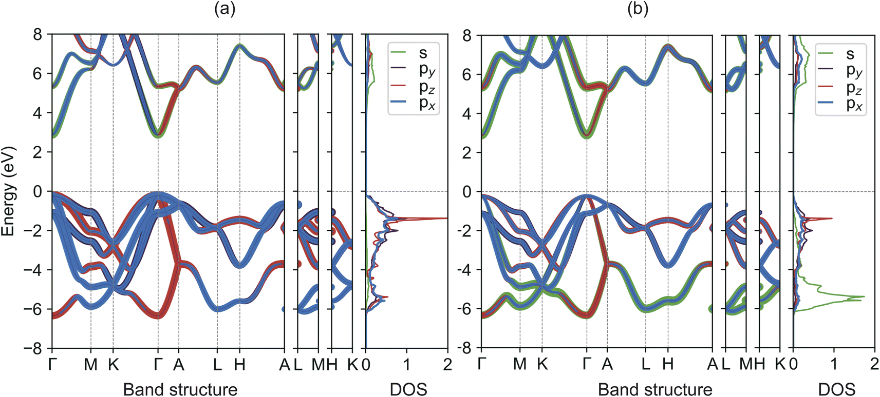 | ||
| Fig. 2 (Color online) TB-mBJ calculated orbital-projected band structures and density of states for (a) Ga and (b) N atoms in w-GaN. The Fermi level is set to zero. | ||
In our investigation of the local environment's influence on the lattice constant and band gap bowing parameters in disordered GaxIn1−xN alloys, we computed five inequivalent disordered and one ordered alloy configurations. Fig. 3(a) and (b) plot the PBE-calculated lattice constants a(x) and c(x) of GaxIn1−xN as functions of Ga content. We observe a linear decrease in a(x) with increasing Ga content, exhibiting a negligible bowing parameter b of approximately 0.005 Å for random alloys and 0.04 Å for ordered alloys. However, a slight deviation of about 0.02 Å is noticed in the lattice constant c(x). Conversely, the TB-mBJ calculated band gap energy shows a distinctly nonlinear variation with alloy composition, featuring an average bowing parameter b as high as 2.66 eV. Significant discrepancies have been noted in the experimental values of b, ranging from 1.4 eV to 2.8 eV,1,16–19 especially following the reassessment of the InN band gap.18,20 Despite the nonlinearity, the band gap energy changes continuously with varying alloy composition and can be fine-tuned to desired intermediate values by adjusting the In to Ga ratio. Additionally, the bowing parameters for both lattice constant and band gap remain largely unaffected by the distribution of alloy constituents. We present the PBE-calculated mixing enthalpy versus Ga concentration for random and ordered alloys in Fig. 3(d). It is found that the mixing enthalpies show a parabolic-like concentration dependence increase monotonically when changing the concentration of Ga from 0% to 50%. At an In concentration of 50%, the mixing enthalpy of the disordered configuration is energetically more favorable than the corresponding the ordered one by 0.15 eV per cell, suggesting that the phase separation phenomenon could be observed as pointed by the previous experimental studies.5,58–60 Furthermore, the mixing enthalpy difference between five unequivalently disordered is less than 0.02 eV per cell, implying that the random disordered effect has little influence on spatial separation.
 | ||
| Fig. 3 (Color online) calculated (a) lattice constant a, (b) lattice constant b, (c) band gap Eg, and (d) mixing-enthalpy as functions of Ga concentration in GaxIn1−xN alloys, examining both disordered and ordered alloy configurations. | ||
For further insight into the band gap bowing characteristics, we evaluated the band-edge positions in GaxIn1−xN relative to the core-level state.46,47 This entailed assuming a constant energy difference between the VBM and CBM and using the N-2s core-level states as reference in the band offset calculations. As depicted in Fig. 4, the valence-band edges exhibit minimal variation with Ga concentration, while most changes are observed in the CBM. The bowing parameters for the absolute positions of VBM and CBM are 0.1 and 1.0 eV, respectively. The nonlinear variation of the band gap as a function of Ga concentration can be attributed to the distinct slopes seen in the absolute positions of VBM and CBM relative to Ga concentration.
 | ||
| Fig. 4 (Color online) TB-mBJ calculated (a) band offsets and (b) positions of CBM and VBM as functions of Ga concentration in GaxIn1−xN alloys, employing core-level alignment. | ||
To juxtapose the electronic structures of alloyed systems with their unalloyed counterparts, we focus on Ga0.5In0.5N alloys as a representative example. The unfolded band structures for both ordered and disordered Ga0.5In0.5N alloys, as derived using the TB-mBJ method, are depicted in Fig. 5(a) and (b). Among these, the ordered Ga0.5In0.5N alloy preserves Bloch characters effectively over a broad energy range [−8, 8] eV near the Fermi level. In contrast, the band dispersions in the disordered configurations are notably disrupted. Two factors contribute to this mild effect on the band structure of disordered alloys. First, the differing atomic radii of Ga and In lead to local lattice distortions upon interchange, affecting the overall structure. Second, the varying energy levels of their valence electrons, due to distinct electronegativities, further influence the electronic properties. Nevertheless, despite these local distortions, Bloch characters near the VBM and CBM are meticulously maintained, resulting in minimal scattering of charge carriers.
 | ||
| Fig. 5 (Color online) TB-mBJ calculated unfolded band structure of (a) ordered and (b) disordered Ga0.5In0.5N alloy derived from a 3 × 3 × 2 supercell unfolded to a primitive Bloch representation. The Fermi level is set to zero. | ||
Both GaN and InN, belonging to the 6mm point group, exhibit five independent elastic-stiffness coefficients. The 6 × 6 matrix of elastic constants Cij for crystals with a wurtzite structure is given by
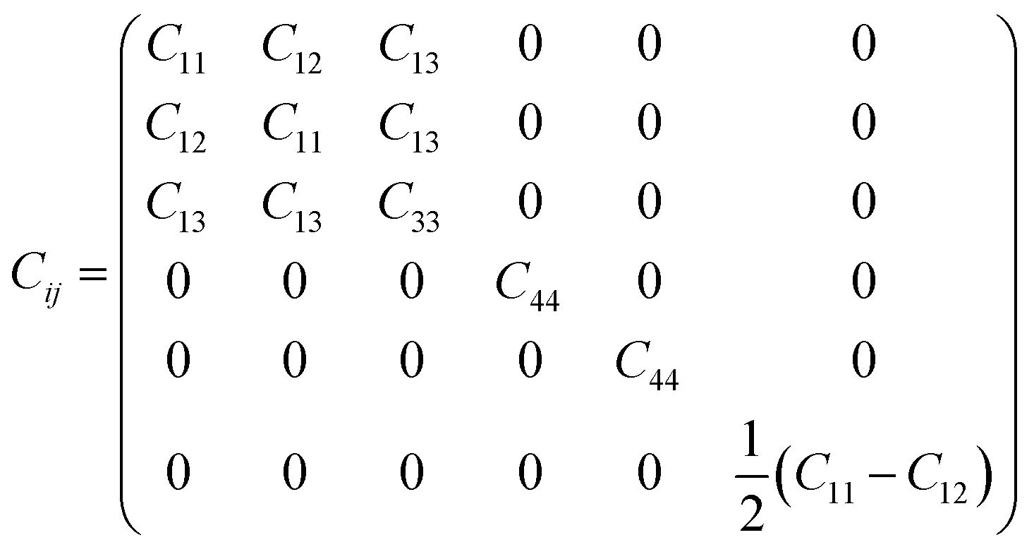 | (2) |
We derived the elastic stiffness constants using the energy-strain method with the PBE functional, extracting the elastic stiffness tensor from the second-order derivative of the total energy plotted against strain curves, in line with methodologies from our previous studies.48 The strain varied between −1.5% and 1.5% in increments of 0.5%. The bulk modulus B0, Young's modulus E, and Poisson's ratio ν of a wurtzite material are calculated using49
 | (3) |
 | (4) |
 | (5) |
The elastic constants and modulus calculated for GaxIn1−xN are presented in Fig. 6(a) and summarized in Table 1. We observe a monotonic decrease in all elastic properties with increasing Ga composition (x), attributable to the stronger bonding in Ga–N compared to In–N, resulting in greater covalence in Ga–N. Notably, the composition dependencies of C11, C33, and E display pronounced sub-linear behavior, characterized by bowing parameters of 78.2 GPa, 124.5 GPa, and 120.7 GPa, respectively. Similarly, C13, C33, and B0 also exhibit sub-linear trends, with bowing parameters of 12.1 GPa, 21.0 GPa, and 36.1 GPa, respectively. In contrast, C12 and ν demonstrate a Vegard-like dependence. It is notable that the calculated values of C11, C33, and E under uniaxial strain show sensitivity to compositional changes, highlighting the impact of varying compositions on these elastic properties. However, the elastic constants calculated using the PBE method for GaxIn1−xN are slightly underestimated compared to experimental values, primarily due to the under-binding effect.50
 | ||
| Fig. 6 (Color online) calculated (a) elastic constants Cij (GPa) and (b) piezoelectric coefficients ekl (C m−2) of disordered GaxIn1−xN alloys as functions of Ga molar fraction. The values of the bulk modulus, Young's modulus, and Poisson's ratio are also presented. | ||
| x | a | c | Eg | C11 | C12 | C13 | C33 | C44 | B0 | E | ν | e15 | e31 | e33 |
|---|---|---|---|---|---|---|---|---|---|---|---|---|---|---|
| 0 | 3.60 | 5.79 | 0.90 | 210.67 | 112.64 | 94.80 | 212.50 | 45.34 | 137.44 | 156.91 | 0.29 | −0.49 | −0.55 | 1.12 |
| 0 (expt.51) | 3.54 | 5.72 | 0.7 | 190 | 104 | 121 | 182 | 10 | 140 | — | — | — | −0.57 | 0.97 |
| 25 | 3.50 | 5.65 | 1.08 | 236.26 | 112.53 | 99.31 | 232.21 | 53.40 | 147.29 | 175.66 | 0.28 | −0.34 | −0.54 | 0.96 |
| 50 | 3.42 | 5.51 | 1.58 | 255.56 | 131.15 | 104.26 | 264.78 | 61.83 | 161.56 | 208.56 | 0.27 | −0.44 | −0.65 | 1.05 |
| 75 | 3.32 | 5.39 | 2.15 | 291.66 | 134.70 | 105.78 | 313.14 | 73.33 | 176.54 | 260.65 | 0.23 | −0.29 | −0.46 | 0.88 |
| 100 | 3.23 | 5.25 | 3.50 | 343.08 | 141.02 | 117.30 | 379.46 | 89.04 | 201.83 | 322.62 | 0.24 | −0.14 | −0.42 | 0.78 |
| 100 (expt.52) | 3.16 | 5.12 | 3.50 | 390 | 145 | 106 | 398 | 105 | 210 | — | — | −0.30 | −0.33 | 0.65 |
| b | 0.01 | 0.02 | 2.66 | 78.23 | −2.54 | 12.09 | 124.59 | 21.01 | 36.10 | 120.71 | 0.00 | −0.29 | −0.01 | −0.19 |
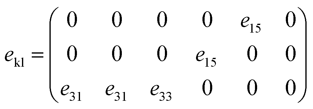
The piezoelectric polarization for hexagonal materials within the C6v crystallographic point group includes three independent piezoelectric coefficients, represented by
 | (6) |
In this study, the piezoelectric stress coefficients ekl are calculated using the density functional perturbation theory (DFPT) method.53 The symmetrized piezoelectric tensor components ekl, in units of C m−2, for GaxIn1−xN are illustrated in Fig. 6(b) and summarized in Table 1. Notably, both e33 and e15 demonstrate a significant reduction in magnitude, decreasing from 1.12 and 0.49 to 0.78 and 0.14, respectively. This trend indicates a substantial deviation from linear dependence on composition. Conversely, e33 shows a weak compositional dependence due to its closeness in value to both GaN and InN. However, it is observed that the PBE method tends to slightly overestimate piezoelectric coefficients when compared to experimental values, a discrepancy attributed to PBE's limitations in accurately describing the electronic contributions to the piezoelectric response.
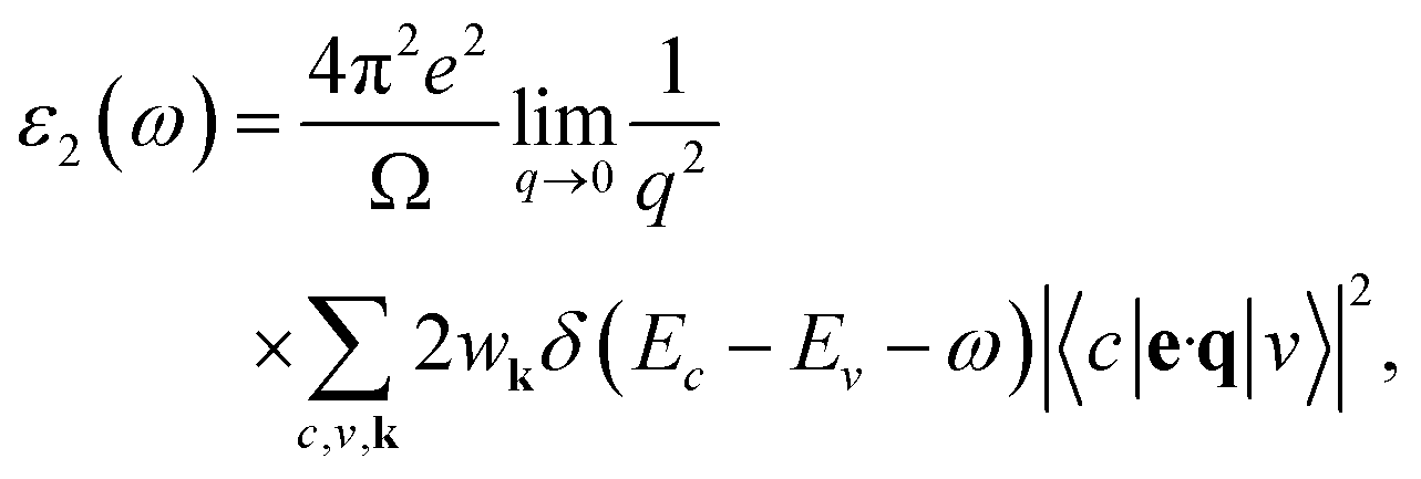
The optical properties of solids are crucial in the analysis and design of optoelectronic devices, including light sources and detectors. These properties emerge from electronic excitations within crystals exposed to electromagnetic radiation. In the linear response regime, we often characterize optical properties comprehensively through the complex dielectric function, expressed as ε(ω) = ε1(ω) + iε2(ω). Here, ω signifies the frequency of incident photons, with ε1(ω) and ε2(ω) representing the dielectric function's real and imaginary parts, respectively. Typically, the dielectric function encompasses two main contributions: intraband and interband transitions. Intraband transitions are especially relevant for metals, while interband transitions can be categorized as either direct or indirect. Indirect interband transitions involve phonon scattering and generally have a lesser impact on ε(ω) in comparison to direct transitions. Therefore, in our calculations, we focus exclusively on direct transitions. The imaginary part of the dielectric function, ε2(ω), indicative of absorption behavior, is derived from the momentum matrix elements between the valence and conduction wave functions:54,55
 | (7) |
 | (8) |
 | (9) |
 | (10) |
 | (11) |
 | (12) |
 | (13) |
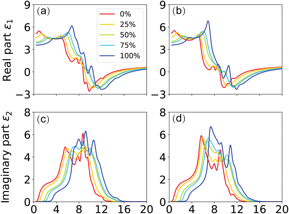
In this context, n is the refractive index, and k represents the extinction coefficient. As the most comprehensive property of a material, the dielectric function elucidates how a material reacts to incident electromagnetic waves. The frequency-dependent ε(ω) for GaxIn1−xN alloys, calculated at the TB-mBJ level for photon energies up to 20 eV and with compositions ranging from 0% to 100%, reveals valuable insights. To analyze the dielectric function, we divide it into two components, εxx(ω) and εzz(ω), corresponding to polarization vectors perpendicular and parallel to the crystallographic c-axis. By comparing these curves, a slight anisotropy is observed across the crystal structure for all compositions, as illustrated in Fig. 7.
 | ||
| Fig. 7 (Color online) TB-mBJ calculated (a) εxx1(ω), (b) εzz1(ω), (c) εxx2(ω) and (d) εzz2(ω) of the dielectric function. | ||
For example, in Fig. 7(c), the threshold energy for pure GaN (x = 100%) is shown to occur at 3.0 eV in the εxx2(ω) curve, closely mirroring the calculated band gap and marking the fundamental absorption edge of GaN. This finding confirms direct optical transitions between the valence band maxima and conduction band minima at the Γ point. The dielectric function's real part, ε1, remains positive up to 9.1 eV, facilitating photon propagation through the alloy. In contrast, when ε1 falls below zero, it indicates attenuation of the electromagnetic wave, and at ε1 = 0, only longitudinally polarized waves can exist. With increasing energy, GaN's imaginary part of the dielectric function exhibits four major peaks at approximately 7.0 eV, 7.7 eV, 8.9 eV, and 10.4 eV, aligning well with available experimental values.17
The Partial Joint Density of States (JDOS) of GaN, as depicted in Fig. 8(a), indicates that the first peak of optical absorption, spanning 2 to 7 eV, is predominantly dictated by transitions from the highest valence band to the lowest conduction band (VB1 → CB1). The second peak in the 5.5–9.5 eV range mainly results from the VB1 → CB2 transition, while the fourth peak in the 9.5–12.5 eV range is primarily due to the VB1 → CB4 transition. Additionally, the third peak in the 5–12 eV range largely stems from the VB3 → CB2 transition. Fig. 8(b) highlights the probability of transitions between states, with a higher Transition Dipole Moment (TDM) indicating a greater likelihood of transition between two states. A zero TDM value suggests forbidden transitions. Notably, the peak TDM value between the VB1 and CB1 states is situated at the Γ point, and the main contribution to the VB1 and CB2 transition is near the M point. Furthermore, both the VB3 → CB2 and VB1 → CB4 transitions are allowed along most of the k-path, except at the Γ, M, and K points.
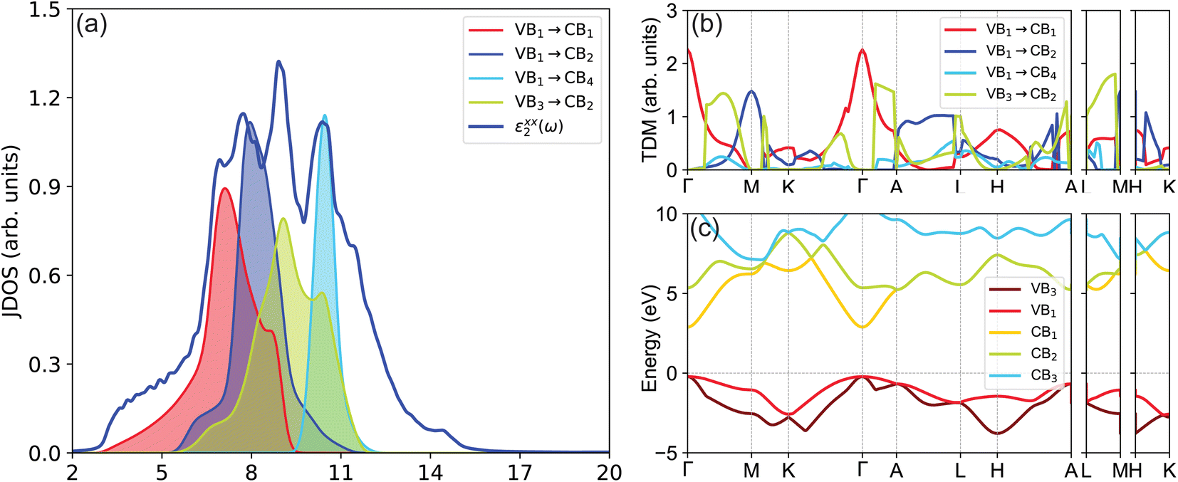 | ||
| Fig. 8 (Color online) (a) TB-mBJ calculated partial joint density of states, (b) transition dipole moment, and (c) band structure of GaN. The allowed and forbidden transitions are shown by solid and dashed arrows, respectively. | ||
The static dielectric constant, ε∞, crucially represents the electronic contribution to the dielectric response of a material. This constant is estimated by extrapolating ε1(ω) to the limit as the frequency, ω, approaches zero. It's pertinent to note that this estimation omits the ionic contributions to the dielectric screening, which stem from the response of ions or atoms in the polar material to the applied electric field. Examination of Fig. 7(a) and (b) reveals a decrease in the calculated values of εxx∞ and εzz∞ from 5.08 (5.12) to 3.57 (3.58), corresponding to the increase in Ga composition from 0% (InN) to 100% (GaN) at zero photon energy. This trend is indicative of a slight sublinear behavior, as shown in Fig. 10(a), with bowing parameters of 0.57 for εxx∞ and 0.63 for εzz∞. Interestingly, these values are somewhat lower than the experimental values of 5.2 for GaN and 8.4 for InN, as cited in Ref. 39. The dependence of the dielectric function on the energy gap is in line with the Penn model,61 suggesting that the dielectric function increases as the band gap narrows. In the ultraviolet spectrum above 16 eV, the real part of ε1(ω) nears unity, while the imaginary part, ε2(ω) becomes almost negligible, indicating that GaxIn1−x N alloys are essentially transparent with minimal absorption in this range.
 | ||
| Fig. 9 (Color online) TB-mBJ calculated (a and f) absorption, (b and g) refractive, (c and h) extinction coefficient (d and i) reflectivity, and (e and j) energy-loss function for the electric field vector parallel (a–e) and perpendicular (f–j) to the crystallographic c-axis, respectively. | ||
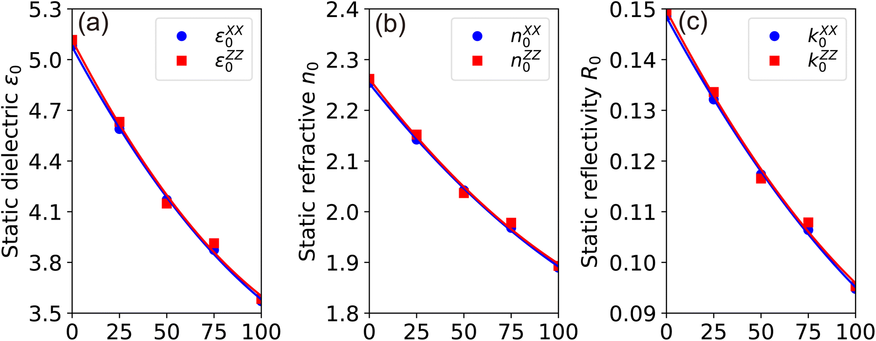 | ||
| Fig. 10 (Color online) TB-mBJ calculated (a) static dielectronic constant ε0, (b) static refractive n0 and (c) static reflectivity k0 as a function of Ga concentration in GaxIn1−xN alloys. | ||
The absorption coefficient, α(ω), delineates the proportion of energy absorbed per unit length as light traverses through a medium. It is evident from Fig. 9(a) that GaxIn1−xN alloys absorb photons in the 1–15 eV energy spectrum, exhibiting heightened absorptivity particularly in the 8–12 eV range. The light absorptivity, while displaying limited anisotropy across different crystallographic axes, reveals that αxx(ω) is marginally greater than αzz(ω). Proximate to the band edge, the absorption coefficient is approximately 1.2 × 105 cm−1, aligning well with experimental results.5 The absorption spectrum experiences a notable shift toward higher photon energies with an increase in Ga content, paralleling the trends observed in band gap, valence, and conduction bands as Ga concentration varies.
The refractive index, n(ω), is an essential optical property of materials, with its real part representing the phase velocity of light within the material. This phase change is quantified as light traverses the material. Conversely, the imaginary part, κ, known as the extinction coefficient, signifies the extent of absorption loss during electromagnetic wave propagation. Their interrelation is expressed by n2 − k2 = ε1. Fig. 9(b) showcases the calculated behavior of n(ω) across different Ga compositions, revealing a consistent pattern of initially decreasing, then increasing to a prominent peak within the 5–7 eV range, followed by a sharp decrease. The static refractive index, n(0), evaluated at zero frequency, exhibits a quasi-linear decrease from 2.25 for InN to 1.89 for GaN, demonstrating the material's varying ability to bend or refract light. However, it is noteworthy that these values are slightly below the experimental measurements of 2.56 for InN and 2.29 for GaN as reported by Madelung et al.39
The extinction coefficient, κ(ω), characterizes a material's aptitude for light absorption and scattering. There exists a conversion relation between the extinction coefficient and the absorption coefficient,  , where λ denotes the wavelength of light in a vacuum. In GaxIn1−xN alloys, κ(ω) exhibits non-monotonic changes with photon energy, peaking in the 8.5–11.0 eV range, influenced by Ga concentration. This indicates that the alloys maximize light absorption in this energy range.
The reflection coefficient, R(ω), measures the ratio of reflected photon energy to the incident photon energy on a surface. As illustrated in Fig. 9(c), R(ω) for GaxIn1−xN alloys initially starts at about 0.1 and gradually peaks to approximately 0.9 at 16 eV in the ultraviolet spectrum. It then sharply declines, indicating enhanced transparency at shorter wavelengths. The low R(ω) values in the lower energy range (≤4 eV) suggest potential applications in transparent coatings in the visible and ultraviolet spectra. The static reflectivity nearly linearly decreases from 0.15 to 0.01 with an increase in Ga content.
The energy loss function, L(ω), is a vital descriptor of the ratio of electron energy loss in materials to the incident electron energy. Peaks in L(ω), shifting from 14 to 17 eV, correspond to energy loss coefficients transitioning from 40 to 50 as Ga content changes from 0% (InN) to 100% (GaN). These shifts align with the abrupt reductions in R(ω), as seen in Fig. 9(c) and (h). Peaks in L(ω) spectra are indicative of plasma resonance, with corresponding frequencies above which the material behaves dielectrically (ε1(ω) > 0) and below which it exhibits metallic properties (ε1(ω) < 0).
Overall, the linear optical properties of GaxIn1−xN alloys remain consistent across all compositions (x = 0%, 25%, 50%, 75%, 100%). A notable trend is observed: the primary maxima in the optical spectra undergo a distinctive blue shift when transitioning from InN to GaN. Furthermore, the optical spectra for light polarized parallel and perpendicular to the crystallographic c-axis exhibit remarkable similarity, with only subtle anisotropy. These findings are in reasonable agreement with other reported experimental and theoretical results.
IV. Summary
In summary, our comprehensive investigation of wurtzite GaxIn1−xN ternary compounds, conducted using density functional theory, has provided substantial insights into their structural, electronic, elastic, piezoelectric, and dielectric properties. We have observed nuanced deviations from Vegard's law, particularly in the band gap, elastic, piezoelectric, and dielectric constants. A notable aspect of our findings is the non-linear relationship between the electronic properties and Ga concentration, especially evident in the varying positions of the valence band maximum and the conduction band minimum as Ga concentration changes. Moreover, our study of the optical characteristics of GaxIn1−xN alloys has revealed a consistent pattern in their linear optical properties across all compositional ranges, characterized by a significant blueshift in the optical spectra. Additionally, we detected a slight anisotropy between the components of the polarization vector, attributable to the differing symmetries in the in-plane and out-of-plane orientations within the wurtzite crystal structure. Overall, these findings enhance our understanding of the structural, electronic, and optical attributes of wurtzite GaxIn1−xN alloys. This advancement is crucial for the further development of doped alloys and their implementation in electronic and optoelectronic technologies. The potential to precisely modify the properties of these alloys paves the way for improved performance and functionality in a variety of applications.Conflicts of interest
There are no conflicts to declare.Acknowledgements
This work is supported by the First-class Discipline Construction (Education Discipline) Funding Program for Higher Education Institutions in Ningxia (Program No. NXYLXK2021B10). L. Q. X. acknowledges the financial support from the Natural Science Foundation of China (No. 12164036), the Natural Science Foundation of Ningxia of China (No. 2020AAC03271), and the Youth Talent Training Project of Ningxia of China (2016). H. B. N. acknowledges the financial support from the Natural Science Foundation of Shannxi Province of China (No. 2021JM-541) and The Youth Innovation Team of Shaanxi Universities. In addition, this work was also partly supported by the Natural Science Basic Research Program of Shaanxi (Program No. 2022JQ-063 and 2021JQ-464). X. F. X. acknowledges the financial support from National Natural Science Foundation of China (61965001), the Ningxia Province Key Research and Development Program (No. 2021BEE03005), the Ningxia key Natural Science Foundation Project (No. 2023AAC02045), the Ningxia First-Class Discipline and Scientific Research Projects (electronic science and technology, No. NXYLXK2017A07-DKPD2023C10 and DKPD2023D01).References
- I. Vurgaftman and J. R. Meyer, J. Appl. Phys., 2003, 94, 3675 CrossRef CAS.
- J. Wu, J. Appl. Phys., 2009, 106, 011101 CrossRef.
- I. L. Guy, S. Muensit and E. M. Goldys, Appl. Phys. Lett., 1999, 75, 4133 CrossRef CAS.
- C. Pan, L. Dong, G. Zhu, S. Niu, R. Yu, Q. Yang, Y. Liu and Z. L. Wang, Nat. Photonics, 2013, 7, 752 CrossRef CAS.
- R. Singh, D. Doppalapudi, T. D. Moustakas and L. T. Romano, Appl. Phys. Lett., 1997, 70, 1089 CrossRef CAS.
- J. W. Orton and C. T. Foxon, Rep. Prog. Phys., 1998, 61, 1 CrossRef CAS.
- S. Nakamura, Semicond. Sci. Technol., 1999, 14, R27 CrossRef CAS.
- J. Wu, W. Walukiewicz, K. M. Yu, W. Shan, J. W. A. III, E. E. Haller, H. Lu, W. J. Schaff, W. K. Metzger and S. Kurtz, J. Appl. Phys., 2003, 94, 6477 CrossRef CAS.
- F. Yam and Z. Hassan, Superlattices Microstruct., 2008, 43, 1 CrossRef CAS.
- C. J. Neufeld, N. G. Toledo, S. C. Cruz, M. Iza, S. P. DenBaars and U. K. Mishra, Appl. Phys. Lett., 2008, 93, 143502 CrossRef.
- R. Dahal, B. Pantha, J. Li, J. Y. Lin and H. X. Jiang, Appl. Phys. Lett., 2009, 94, 063505 CrossRef.
- X. Zheng, R.-H. Horng, D.-S. Wuu, M.-T. Chu, W.-Y. Liao, M.-H. Wu, R.-M. Lin and Y.-C. Lu, Appl. Phys. Lett., 2008, 93, 261108 CrossRef.
- K. Fujii, T. Karasawa and K. Ohkawa, Jpn. J. Appl. Phys., 2005, 44, L543 CrossRef CAS.
- J. Li, J. Y. Lin and H. X. Jiang, Appl. Phys. Lett., 2008, 93, 162107 CrossRef.
- I. Waki, D. Cohen, R. Lal, U. Mishra, S. P. DenBaars and S. Nakamura, Appl. Phys. Lett., 2007, 91, 093519 CrossRef.
- K. P. O'Donnell, R. W. Martin, C. Trager-Cowan, M. E. White, K. Esona, C. Deatcher, P. G. Middleton, K. Jacobs, W. Van der Stricht, C. Merlet, B. Gil, A. Vantomme and J. F. W. Mosselmans, Mater. Sci. Eng. B, 2001, 82, 194 CrossRef.
- E. Sakalauskas, Ö. Tuna, A. Kraus, H. Bremers, U. Rossow, C. Giesen, M. Heuken, A. Hangleiter, G. Gobsch and R. Goldhahn, Phys. Status Solidi B, 2012, 249, 485 CrossRef CAS.
- J. Wu, W. Walukiewicz, K. M. Yu, J. W. Ager III, E. E. Haller, H. Lu and W. J. Schaff, Appl. Phys. Lett., 2002, 80, 4741 CrossRef CAS.
- M. Moret, B. Gil, S. Ruffenach, O. Briot, C. Giesen, M. Heuken, S. Rushworth, T. Leese and M. Succi, J. Cryst. Growth, 2009, 311, 2795 CrossRef CAS.
- J. Wu, W. Walukiewicz, K. M. Yu, J. W. A. III, E. E. Haller, H. Lu, W. J. Schaff, Y. Saito and Y. Nanishi, Appl. Phys. Lett., 2002, 80, 3967 CrossRef CAS.
- Z. Dridi, B. Bouhafs and P. Ruterana, Semicond. Sci. Technol., 2003, 18, 850 CrossRef CAS.
- J. Song, Z. Luo, X. Liu, E. Li, C. Jiang, Z. Huang, J. Li, X. Guo, Z. Ding and J. Wang, Crystals, 2020, 10, 1159 CrossRef CAS.
- P. Carrier and S.-H. Wei, J. Appl. Phys., 2005, 97, 033707 CrossRef.
- B. Lee and L. W. Wang, J. Appl. Phys., 2006, 100, 093717 CrossRef.
- X. Ruan, F. Zhang and W. Zhang, J. Theor. Comput. Chem., 2014, 13, 1450070 CrossRef CAS.
- J. L. Lyons, A. Janotti and C. G. Van de Walle, Phys. Rev. B: Condens. Matter Mater. Phys., 2014, 89, 035204 CrossRef.
- S. Zhang, J.-J. Shi, M. Zhang, M. Yang and J. Li, J. Phys. D: Appl. Phys., 2011, 44, 495304 CrossRef.
- P. G. Moses and C. G. Van de Walle, Appl. Phys. Lett., 2010, 96, 021908 CrossRef.
- G. Kresse and J. Furthmüller, Phys. Rev. B: Condens. Matter Mater. Phys., 1996, 54, 11169 CrossRef CAS PubMed.
- G. Kresse and J. Furthmüller, Comput. Phys. Sci., 1996, 6, 15 CAS.
- P. E. Blöchl, Phys. Rev. B: Condens. Matter Mater. Phys., 1994, 50, 17953 CrossRef PubMed.
- G. Kresse and D. Joubert, Phys. Rev. B: Condens. Matter Mater. Phys., 1999, 59, 1758 CrossRef CAS.
- J. P. Perdew, K. Burke and M. Ernzerhof, Phys. Rev. Lett., 1996, 77, 3865 CrossRef CAS PubMed.
- F. Tran and P. Blaha, Phys. Rev. Lett., 2009, 102, 226401 CrossRef PubMed.
- A. D. Becke and E. R. Johnson, J. Chem. Phys., 2006, 124, 221101 CrossRef PubMed.
- H. Jiang, J. Chem. Phys., 2013, 138, 134115 CrossRef PubMed.
- F. Fuchs, J. Furthmüller, F. Bechstedt, M. Shishkin and G. Kresse, Phys. Rev. B: Condens. Matter Mater. Phys., 2007, 76, 115109 CrossRef.
- M. Shishkin and G. Kresse, Phys. Rev., 2007, 75, 235102 Search PubMed.
- O. Madelung, Semiconductors: Data Handbook, Springer Science & Business Media, 2012 Search PubMed.
- A. Zunger, S.-H. Wei, L. G. Ferreira and J. E. Bernard, Phys. Rev. Lett., 1990, 65, 353 CrossRef CAS PubMed.
- S.-H. Wei, L. G. Ferreira, J. E. Bernard and A. Zunger, Phys. Rev. B: Condens. Matter Mater. Phys., 1990, 42, 9622 CrossRef CAS PubMed.
- V. Popescu and A. Zunger, Phys. Rev. Lett., 2010, 104, 236403 CrossRef PubMed.
- V. Popescu and A. Zunger, Phys. Rev. B: Condens. Matter Mater. Phys., 2012, 85, 085201 CrossRef.
- V. Wang, N. Xu, J.-C. Liu, G. Tang and W.-T. Geng, Comput. Phys. Commun., 2021, 267, 108033 CrossRef CAS.
- L. Vegard, Z. Phys., 1921, 5, 17 CrossRef CAS.
- E. A. Kraut, R. W. Grant, J. R. Waldrop and S. P. Kowalczyk, Phys. Rev. Lett., 1980, 44, 1620 CrossRef CAS.
- Z. Zhang, Y. Guo and J. Robertson, Appl. Phys. Lett., 2019, 114, 161601 CrossRef.
- V. Wang and W. T. Geng, J. Phys. Chem. C, 2017, 121, 10224 CrossRef CAS.
- J.-M. Wagner and F. Bechstedt, Phys. Rev. B: Condens. Matter Mater. Phys., 2002, 66, 115202 CrossRef.
- S. P. Łepkowski, J. A. Majewski and G. Jurczak, Phys. Rev. B: Condens. Matter Mater. Phys., 2005, 72, 245201 CrossRef.
- V. Siklitsky, A. Tolmatchev, V. Bougrov, M. Levinshtein, S. Rumyanstev and A. Zubrilov, 2023, available online, https://www.ioffe.ru/SVA/NSM/Semicond/InN/, accessed on 18 December 2023.
- V. Siklitsky, A. Tolmatchev, V. Bougrov, M. Levinshtein, S. Rumyanstev and A. Zubrilov, 2023, available online, https://www.ioffe.ru/SVA/NSM/Semicond/GaN/, accessed on 18 December 2023.
- X. Wu, D. Vanderbilt and D. R. Hamann, Phys. Rev. B: Condens. Matter Mater. Phys., 2005, 72, 035105 CrossRef.
- H. Ehrenreich and M. H. Cohen, Phys. Rev., 1959, 115, 786 CrossRef.
- M. Gajdoš, K. Hummer, G. Kresse, J. Furthmüller and F. Bechstedt, Phys. Rev. B: Condens. Matter Mater. Phys., 2006, 73, 045112 CrossRef.
- J. S. Toll, Phys. Rev., 1956, 104, 1760 CrossRef.
- A. M. Fox, Optical Properties of Solids, Oxford University Press, 2001, vol. 3 Search PubMed.
- M. D. McCluskey, L. T. Romano, B. S. Krusor, D. P. Bour, N. M. Johnson and S. Brennan, Appl. Phys. Lett., 1998, 72, 1730 CrossRef CAS.
- C. Kisielowski, Z. Liliental-Weber and S. Nakamura, Jpn. J. Appl. Phys., 1997, 36, 6932 CrossRef CAS.
- I. Ho and G. B. Stringfellow, Appl. Phys. Lett., 1996, 69, 2701 CrossRef CAS.
- D. R. Penn, Phys. Rev., 1962, 128, 2093 CrossRef CAS.
| This journal is © The Royal Society of Chemistry 2024 |