DOI:
10.1039/D3RA08607K
(Paper)
RSC Adv., 2024,
14, 1538-1548
Thermodynamic, electronic, and optical properties of ultra-wide bandgap zirconium-doped tin dioxide from a DFT perspective
Received
17th December 2023
, Accepted 19th December 2023
First published on 3rd January 2024
Abstract
The effects of zirconium doping on the thermodynamic, electronic, and optical properties of tin dioxide are investigated by using density functional theory calculations combined with the cluster expansion method. In the whole composition range, the formation enthalpies of all structures are positive, indicating that SnO2–ZrO2 is an immiscible system and the ZrSnO2 alloy has a tendency of phase separation at low temperature. The x-T phase diagram of ZrSnO2 ternary alloy shows that the critical temperature is 979 K, which means that when the growth temperature of ZrSnO2 crystal is higher than the critical temperature, it is possible to realize the full-component solid solution. The bandgaps of ZrxSn1−xO2 alloys (0 ≤ x ≤ 1) are direct and increase as the Zr composition increases. Zr doping can tune the bandgap of SnO2 from the ultraviolet-B region to the deep ultraviolet region, and has a strong optical response to deep ultraviolet light. The projected density of states and band offsets clearly reveal the reason for the increase of bandgap, which provides useful information to design relevant optoelectronic devices such as quantum wells and solar-blind deep ultraviolet photodetectors.
1. Introduction
Semiconductor deep ultraviolet (UV) optoelectronic devices have great application prospects in the fields of the national economy and people's livelihoods, military defense, and other fields, and can be widely used in laser precision processing, precision measurement, semiconductor lithography processes, biomedicine, water and air detection and purification, heat source detection, etc.1–3 Therefore, ultra-wide bandgap semiconductor materials with a band gap of more than 4.5 eV have gradually attracted the attention of researchers from all over the world. Common ultra-wide bandgap semiconductor materials include aluminum nitride (6.2 eV), diamond (5.5 eV), β-Ga2O3 (4.8 eV), SnO2 (3.6 eV), etc. Although some progress has been made in the research of ultra-wide bandgap semiconductor materials, there are still some problems e.g. that the AlxGa1−xN system is prone to phase separation and composition segregation under high Al content. At the same time, the donor and acceptor levels will become deeper and difficult to excite; due to the continuous photoconductivity effect, the response time of AlGaN-based UV photodetectors is difficult to improve.4 High quality and large area epitaxial growth of diamond has been difficult, and there is no effective bandgap adjustment method. The p-type doping of β-Ga2O3 is very difficult due to its band structure.5
Due to the bandgap of 3.6 eV in SnO2, it can be used as a UV-B band photodetector. F-doped SnO2 has been widely used as a transparent conductive material in fields such as LEDs and solar cells.6,7 Li et al. improved the luminous efficiency of SnO2 by doping In in SnO2, and achieved near UV electroluminescence at 398 nm.8 At the same time, they also found that Ag doping can form acceptors and achieve near-band edge luminescence at 361–375 nm. In addition, the transformation of SnO2 from n-type to p-type can be achieved by heavily doping Mg in SnO2, and strong UV luminescence can be observed in photoluminescence experiments.9,10 Xue et al. achieved ultra-wide response photodetectors in the 365 nm to 980 nm wavelength range by growing SnO2 on p-type Si.11 However, limited by the bandgap of SnO2 (3.6 eV), the minimum cutoff wavelength of the above devices is about 320 nm, which can only achieve visible light-blind UV detection, and it is difficult to achieve solar-blind deep UV detection. In SnO2, both 5s and 5p electrons of Sn are transferred to the O atom, resulting in empty bands of 5s and 5p, forming the conduction band minimum (CBM). The 4d band of Sn is in a full band state, located below the valence band maximum (VBM). The VBM of SnO2 is composed of the 2p orbital of O. By doping Zr to partially replace Sn, the unfilled Zr-4d orbital and O-2p orbital are hybridized to form the VBM, thereby changing the symmetry of the VBM and achieving efficient optoelectronic conversion. In addition, the ionic radius of Zr4+ (0.79 Å) is slightly larger than that of Sn4+ (0.69 Å), hence the similar ionic radius means Zr4+ ions can easily replace Sn4+ ions in the crystal lattice, and the product compound can stabilize the lattice structure. The bandgap of ZrO2 (5–7 eV) is much wider than that of SnO2, which is suitable for forming a ternary alloy with SnO2, increasing the bandgap of SnO2 and achieving band regulation, so as to realize its application in the field of ultra-short wavelength and deep UV photodetectors.
In this paper, the crystal structure, solubility limit, electronic and optical properties of ZrSnO2 alloy are systematically studied by first-principles calculations combined with the cluster expansion method. The variation trend and regulation mechanism of the bandgap of the alloy caused by Zr doping are revealed. This will provide meaningful guidance and reference for the band engineering of SnO2 and its potential application in solar-blind deep UV detectors in theory and technology.
2. Computational methodologies
The cluster expansion (CE) method is performed by the MIT Ab initio Phase Stability (MAPS) program in the Alloy Theoretic Automated Toolkit (ATAT)12 to generate ZrxSn1−xO2 alloy configurations with different doping contents, and quickly fit the energies of a small portion of configurations calculated by DFT to obtain the formation enthalpies for all configurations. The CE method has been successfully applied to the study of various alloy systems, such as PdHx,13 MgxNi1−xO,14 CdSxSe1−x,15 and ZnS1−xSex.16 In principle, the ZrxSn1−xO2 alloy phase equilibrium and ground state calculations require one to determine the total energies of all possible configurations. However, it is costly and unrealistic to calculate the total energies of all possible configurations via first-principles calculations. An Ising-like Hamiltonian can be constructed via the CE method to determine the energies of different alloy configurations. It can rapidly calculate the energy of any alloy configuration and thus saves significant computation time. Here, we give a generalized description of the CE method. The Ising-like Hamiltonian for the energies of possible configurations σ is calculated using| |
 | (1) |
where the J's (Ji, Jij, Jijk, etc.) denote the interaction energies (effective cluster interactions) and Ŝi (i = 1, 2, …, N) are the “spin” variables. Ŝi take the value of +1 or −1 corresponding to the i site occupied by a Sn or Zr atom. The interaction energies J's are obtained by fitting the results of DFT calculations. In this work, 25 alloy configurations are calculated by DFT to obtain the interaction energies. Once the J's are obtained, the energy of any configuration can be rapidly computed using eqn (1). In the process of CE, the MAPS procedure is performed continuously by gradually increasing the number of clusters contained in the CE until the desired precision is reached. The predictive power of the CE method is controlled by the so-called cross-validation (CV) score, which is often defined by comparing the difference between the DFT-calculated energies EDFTi and the fitted energies Efiti from the CE method| |
 | (2) |
A small CV score provides a basis for the power of the CE method. We can consider the CE to be suitable when a CV score of less than 100 meV per cation appears. In this work, the CV score is less than 0.73 meV per cation. We have added a detailed description of the CE method in the computational methodology section of the revised manuscript.
The structural relaxation and property characterization were performed using the first-principles calculation program Quantum Espresso.17 The ultrasoft pseudopotentials (USPPs)18 method was used to describe the interaction between ions and electrons, and the generalized gradient approximation in Perdew–Burke–Ernzerhof (PBE)19 form was used as the exchange correlation function to handle the interaction between electrons. A plane wave energy cutoff of 600 eV was applied in the entire calculation. The convergence thresholds for energy and atomic forces in the self-consistent calculation were set to be less than 0.05 GPa and 1.4 × 10⁻⁵ eV, respectively. Due to strong onsite Coulomb interaction of Zr-4d orbital, the PBE+U strategy was adopted to describe the Coulomb and exchange correlation effects of Zr-4d orbital. An effective U value of 4 eV![[thin space (1/6-em)]](https://www.rsc.org/images/entities/char_2009.gif) 20 produced ZrO2 equilibrium lattice parameters of a = b = 3.68 Å and c = 5.22 Å, which are consistent with the experimental values of a = b = 3.61 Å and c = 5.21 Å.21
20 produced ZrO2 equilibrium lattice parameters of a = b = 3.68 Å and c = 5.22 Å, which are consistent with the experimental values of a = b = 3.61 Å and c = 5.21 Å.21
The branch-point energy (BPE) EBP is regarded as an energy reference level for the band alignment in the band offset calculations.22 It can be using
| |
 | (3) |
where
Nk denotes the number of
Γ-centered Monkhorst–Pack
k points in the Brilloun zone.
NCB and
NVB represent the number of conduction bands (CBs) and valences bands (VBs) at
Γ-centered Monkhorst–Pack
k points, respectively, while
εci(
k) and
εvj(
k) are the energies corresponding to the conduction bands and valence bands. In this work, the BPE is computed by averaging the eigenvalues of the two highest valence bands (
NVB = 2) and the lowest conduction band (
NCB = 1). Once the BPE is determined, it is set to zero and all DFT-calculated VBMs and CBMs refer to it. Then, the VBM and CBM band offsets for Zr
xSn
1−xO
2 alloys with different Zr contents can be obtained as follows:
| |
 | (4) |
| |
 | (5) |
where d
Eg =
EΔ-solg −
EGGA+Ug. In the above equation,
EΔ-solg and
EGGA+Ug indicate the band gaps determined using the Δ-sol and GGA+U methods, respectively.
The optical absorption coefficients are calculated based on the imaginary part ε2(ω) of the frequency dependent complex dielectric function ε(ω) = ε1(ω) + iε2(ω) to quantitatively understand their light-harvesting ability. The imaginary part ε2(ω) is first calculated according to the following formula:23
| |
 | (6) |
where |
Mc,v(
k)|
2 denotes the momentum matrix element, and c and v are the conduction and valence band states, respectively. Then the real part
ε1(
ω) is derived from the imaginary part according to the Kramers–Kroning transformation.
24 Finally, we can obtain the optical absorption coefficients
α(
ω)
via the following expression:
25| |
 | (7) |
3. Results and discussion
3.1. Thermodynamic properties
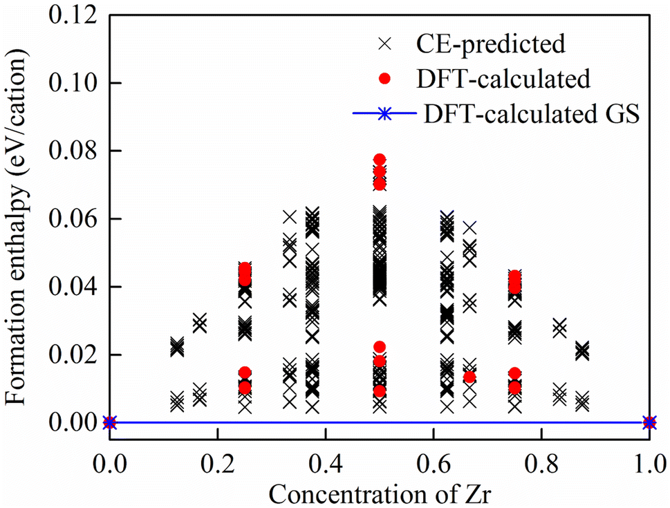
3.1.1. Formation enthalpy and ground-state search. Based on the 25 DFT calculated structures, 670 configurations with different distribution of dopants were searched through CE. Using CE, we estimated the formation enthalpies of all symmetrically independent configurations, accommodating up to 48 atoms in the supercell, as depicted in Fig. 1. Through ground state search, ground state structures are only found at two endpoints (SnO2 and ZrO2), with no other intermediate ground states (the stable ZrxSn1−xO2 alloy configurations with other contents (0 < x < 1) with formation enthalpies below 0, except for x = 0 and 1) present. The formation enthalpies of all ZrxSn1−xO2 alloy configurations are positive, indicating that SnO2 and ZrO2 are difficult to form stable and ordered alloy solid solutions. They exhibit a trend of phase separation at low temperatures, but may form good disordered alloys at high temperatures.
 |
| | Fig. 1 Formation enthalpies of ZrxSn1−xO2 alloys. Black crosses represent CE-predicted energies, red dots denote the DFT-calculated formation enthalpies of selected configurations, and stars mark the two end points SnO2 and ZrO2 as DFT-calculated ground states of ZrxSn1−xO2. | |
3.1.2. Phase diagrams. The thermodynamic phase diagram provides important clues for studying the solubility limit and phase transition temperature of alloys. The binodal curves (the equilibrium solubility limits) are formed via common tangent construction to the Gibbs free energy ΔG at a given temperature and the spinodal curves (the nonequilibrium metastability limits) are made up of the points where the second derivative of ΔG equals zero at a given T. The Gibbs free energy ΔG is defined by| | |
ΔG(x, T) = ΔH(x, T) − TΔS(x)
| (8) |
Here, x is the concentration of Zr, ΔH is the formation enthalpy, and ΔS is the mixing entropy as described by the Bragg–Williams approximation.26 The mixing entropy is given by ΔS = −kB[xlogx + (1 − x) log(1 − x)] per cation. T is the temperature. The binodal and spinodal curves in Fig. 2 divide the phase diagram into the stable, metastable and unstable mixing regions. In the region outside the binodal curve, the ZrxSn1−xO2 solid solutions are single-phase, homogeneous, and stable. The metastable region exists between the binodal and spinodal curves. Phase separation occurs in the region inside the spinodal curve, where the ZrxSn1−xO2 solid solutions are unstable. The critical temperature TC of ZrSnO2 alloy is 979 K, this means that above this temperature, the ZrSnO2 alloy may achieve full-component solid solution. Through advanced semiconductor crystal growth technologies such as metal organic chemical vapor deposition (MOCVD), molecular beam epitaxy (MBE), and pulse laser deposition (PLD), the synthesis of stable ZrSnO2 alloys at high temperatures can be achieved. At present, Zr:SnO2 alloy thin films prepared by spray pyrolysis, chemical vapor deposition and Nb:ZrxSn1−xO2 alloy films prepared by pulsed laser deposition have been reported in the experiment.27–29 The preparation temperatures are 150–200, 400, and 720 °C, respectively. This indicates that ZrxSn1−xO2 alloys are very promising to be prepared experimentally. The application of semiconductor materials under high temperature or extreme conditions is also what people need. Therefore, the stable wide bandgap ZrSnO2 alloys at high temperatures have practical application value and research significance.
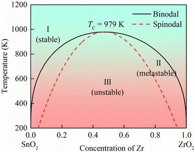 |
| | Fig. 2 The x-T phase diagram of ZrxSn1−xO2 alloys. Solid and dotted lines represent the equilibrium binodal and spinodal curves, respectively. | |
3.2. Electronic properties
3.2.1. Band structures and density of states. To investigate the effect of Zr dopant concentration on the electronic structure, five low-lying configurations with different Zr contents (x = 0, 0.25, 0.5, 0.75, and 1) were select to analyze the variation of bandgap with composition. The crystal structures of five low-lying configurations are shown in Fig. 3. Due to the larger ion radius of Zr, the lattice constants of ZrxSn1−xO2 alloys monotonically increase with the increment of Zr content, as listed in Table 1. The cohesive energies Ec of ZrxSn1−xO2 alloys are calculated using the following formula:| |
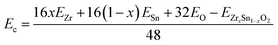 | (9) |
where EZrxSn1−xO2 is the total energy of the ZrxSn1−xO2 alloy, and EZr, ESn, and EO are the energies of an isolated Zr, Sn, and O atom in vacuum, respectively. It can be seen that these ZrxSn1−xO2 alloys have high cohesive energies, indicating that they can theoretically form stable ternary compounds. In addition, it is worth noting that due to the different ionic radii between Zr and Sn atoms, the lattice constants and α, β, γ angles of SnO2 undergo small changes, resulting in lattice distortion, which leads to an orthogonal or monoclinic lattice symmetry in the ZrxSn1−xO2 alloy configuration.
 |
| | Fig. 3 The front views of (a) SnO2, (b) Zr0.25Sn0.75O2, (c) Zr0.5Sn0.5O2, (d) Zr0.75Sn0.25O2, and (e) ZrO2. (a′)–(e′) and (a′′)–(e′′) are the corresponding top and side views in (a)–(e), respectively. The brown, green, and red balls are Sn, Zr, and O atoms, respectively. | |
Table 1 Crystal structure information and cohesive energies (Ec) of ZrxSn1−xO2 (x = 0, 0.25, 0.5, 0.75, and 1) alloys
| ZrxSn1−xO2 |
a (Å) |
b (Å) |
c (Å) |
α (°) |
β (°) |
γ (°) |
Ec (eV per atom) |
| 0 |
9.61 |
9.61 |
6.46 |
90 |
90 |
90 |
5.13 |
| 0.25 |
9.65 |
9.65 |
6.49 |
89.91 |
89.99 |
90.03 |
5.84 |
| 0.5 |
9.68 |
9.72 |
6.49 |
90 |
90 |
90.01 |
6.57 |
| 0.75 |
9.73 |
9.74 |
6.50 |
90 |
90 |
89.99 |
7.28 |
| 1 |
9.77 |
9.77 |
6.52 |
90 |
90 |
90 |
8.01 |
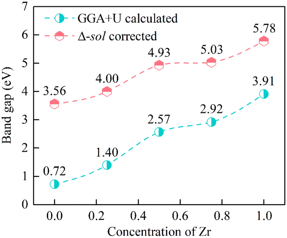
The calculated band structures are shown in Fig. 4, and it can be seen that the VBMs and CBMs of ZrxSn1−xO2 alloys are both located at the Γ point in the Brillouin zone. Therefore, these ZrxSn1−xO2 alloys are direct bandgap semiconductors. As the Zr content increases, the bandgap shows a monotonically increasing trend, with bandgap value ranging from 0.72 to 3.91 eV, as shown in Fig. 5. The distribution of the valence bands is less dispersed than that of the conduction bands because the former has stronger locality. In addition, the CBMs are more dispersive than the VBMs, which means that the effective masses of electrons in the conduction bands are smaller than those of holes in the valence bands. Taking the band structure of Zr0.25Sn0.75O2 as an example, we calculated the effective masses of holes in the VBM and electron in the CBM according to the formula  . The calculated effective masses of electrons and holes are 0.44 m0 and 3.50 m0 (m0 is the mass of an electron), respectively, which confirms that the holes in the valence bands are heavier than the electrons in the conduction bands. Hence, the holes have lower mobility than the electrons. These band structure characteristics also indicate that the O-2p electrons, which form the VBM states (as shown in Fig. 6), are tightly bound to the atoms, reducing the mobility of valence band holes. Thus, although the concentration of conduction band electrons is lower than that of valence band holes, the contribution of electrons to conductivity is greater.
 |
| | Fig. 4 Band structures along the tetragonal high-symmetry directions for (a) SnO2, (b) Zr0.25Sn0.75O2, (c) Zr0.5Sn0.5O2, (d) Zr0.75Sn0.25O2, and (e) ZrO2 calculated at the GGA+U level. The red dotted line is the Fermi level and has been set to zero. | |
 |
| | Fig. 5 GGA+U calculated (cyan circle) and Δ-sol corrected (red hexagon) bandgaps as functions of Zr compositions for ZrxSn1−xO2 alloys. | |
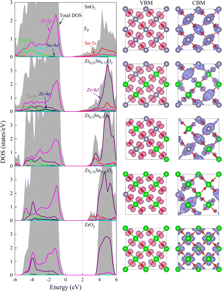 |
| | Fig. 6 Projected density of states (PDOS) and band decomposed charge density distribution of VBM and CBM at Γ point for ZrxSn1−xO2 alloys. The PDOS have been normalized according to the number of atoms in the ZrxSn1−xO2 alloys to better show how it varies with the Zr composition. The red dotted line is the Fermi level and has been set to zero. The isosurface value is 0.01 e Å−3. | |
The underestimations of bandgaps by GGA+U method can be attributed to the inherent self-interaction error and the absence of derivative discontinuity in the exchange–correlation potential.30 To address these issues and diminish discrepancies in the Kohn–Sham energy gap, we implemented the efficient Δ-sol method31 as a correction measure for GGA+U computed bandgaps. The Δ-sol method can significantly improve Kohn–Sham bandgap errors. It estimates the bandgaps of multicomponent alloys by fitting the experimental bandgap values of pure binary compounds, avoiding complex calculations and reducing computational costs. The Δ-sol method has been successfully applied to calculate the bandgaps of various alloy systems.15,16,32 The corrected bandgap is within the range of 3.56 to 5.78 eV, as shown in Fig. 5. This indicates that Zr doping is expected to regulate the bandgap of SnO2 to the deep UV region, so as to realize the application of SnO2-based ultra-wide bandgap solar-blind deep UV photoelectronic devices.
The projected density of states (PDOS) analysis (Fig. 6) shows that before doping with Zr element, the valence and conduction bands near the Fermi level are mainly contributed by the O-2p and Sn-5s states, respectively. After doping with Zr element, the conduction band near the Fermi level is dominated by Zr-4d states, accompanied by some contributions from Sn-5s states. The effect of Zr-4d states on CBM is greater, so the change in band gap value of ZrxSn1−xO2 alloy is mainly caused by Zr doping content. Due to the delocalization of the d-band by GGA exchange–correlation potential, the overlap between the O-2p state and the Sn/Zr-4d state is overestimated, resulting in a severely underestimated bandgap in strongly correlated electronic systems.33 For the conduction band, the lowest unoccupied state near the Fermi level is a mixed state of Sn-5s and Zr-4d. The hybridization of s–d orbitals in the conduction band depends on the relative orbital energies. In fact, the energy difference between the Sn-5s and Zr-4d levels is significant, so as the Zr content increases, the s–d hybridization effect weakens, causing the CBM to move upwards. Therefore, the bandgap of ZrSnO2 alloy gradually widens with the increase of Zr content.
3.2.2. Band offsets. Since Zr doping is bound to affect the electron filling in the VBM and CBM of SnO2, resulting in changes in the position of VBM and CBM. The band offset can intuitively reflect the relative variation of the band alignment of VBM and CBM at the interface of ZrxSn1−xO2 alloys with doping content. It is an crucial parameter for evaluating charge transfer, quantum confinement, and conversion efficiency, and is closely related to the design of optoelectronic devices.22 Therefore, in order to apply ZrxSn1−xO2 alloys as heterojunctions in electronic and optoelectronic devices, the band offsets of VBM and CBM at the interface of ZrxSn1−xO2 alloys with different Zr concentrations were calculated, as show in Fig. 7. The valence band offsets are large, while the conduction band offsets are relatively small. In the tetragonal ZrxSn1−xO2 alloys with Td site symmetry, the anionic 2p and cationic 4d orbitals are equivalent symmetric states, both of which are transformed into Γ15 representation.34,35 The interaction between them generates energy level repulsion, leading to an increase in valence band offset. Due to the higher energy of Zr-4d orbital compared to Sn-4d orbital, as the Zr content increases, the p–d coupling effect becomes more pronounced, leading to a gradual increase in valence band offset.
 |
| | Fig. 7 Band offsets of ZrxSn1−xO2 alloys with different Zr compositions. The branch-point energies are set to zero, treated as reference energy levels, and used to align the conduction and valence band edges. | |
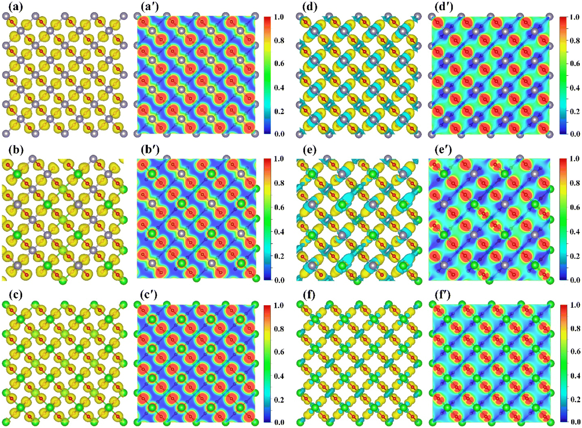
3.2.3. Chemical bonding analysis. From the electron localization function (ELF)36–39 and charge density difference plots (as shown in Fig. 8), it can be seen that there is no charge distribution between metals, which indicates that no bonding interaction exists between them. However, there is a significant amount of charge distribution between the metal and O atoms, and the charge around the metal and O atoms is distributed spherically, indicating that the Sn–O and Zr–O bonds are mainly ionic interactions. According to the Bader charge distribution analysis40–42 (as listed in Table 2), the Bader charges on Sn, Zr, and O atoms are −2.34 to −2.31 |e|, −2.59 to −2.55 |e|, and 1.17–1.27 |e|, respectively. It indicates that Sn and Zr lose electrons, while O gains electrons and charges transfer from Sn and Zr atoms to O atoms. This is consistent with the phenomenon reflected on the charge density difference plots (Fig. 8d–f).
 |
| | Fig. 8 Calculated ELF of (a) SnO2, (b) Zr0.5Sn0.5O2, and (c) ZrO2 alloys in 2 × 2 × 2 supercells at an isosurface value of 0.7 e Å−3. (a′)–(c′) are the sectional plots of corresponding ELF along the (001) plane in (a)–(c). Charge density difference of (d) SnO2, (e) Zr0.5Sn0.5O2, and (f) ZrO2 alloys in 2 × 2 × 2 supercells at an isosurface value of 0.01 e Å−3. The yellow and blue bubbles indicate charge accumulation and depletion, respectively. (d′)–(f′) are the sectional plots of corresponding charge density differences along the (001) plane in (d)–(f). | |
Table 2 The Bader charges of Sn, Zr, and O atoms in ZrxSn1−xO2 alloys. Positive and negative values represent the gain and loss of electrons, respectively
| ZrxSn1−xO2 |
Sn |
Zr |
O |
| 0 |
−2.34 |
— |
1.17 |
| 0.25 |
−2.32 |
−2.59 |
1.19 |
| 0.5 |
−2.31 |
−2.57 |
1.22 |
| 0.75 |
−2.31 |
−2.56 |
1.25 |
| 1 |
— |
−2.55 |
1.27 |
3.3. Optical properties
The effective response of semiconductor materials to light is vital for their applications in optoelectronic and photovoltaic devices. The optical absorption coefficients of ZrxSn1−xO2 alloys were calculated based on the imaginary part of the frequency dependent complex dielectric function. As shown in Fig. 9, the absorption coefficients of ZrxSn1−xO2 alloys exhibit significant optical anisotropy. The absorption edge of pure SnO2 is located in the UV-B spectrum range, with the shortest cutoff wavelength of about 320 nm, which can only achieve visible light- blind UV detection. After the incorporation of Zr element, the adsorption edge shows a notable blue shift. As the Zr content increases from 0 to more than 25%, the absorption edge of the ZrSnO2 alloy gradually shifts to the deep UV region. This is expected to enable the application of solar-blind deep UV photodetectors.
 |
| | Fig. 9 Absorption coefficients of ZrxSn1−xO2 alloys with different Zr compositions for parallel (red) and perpendicular (blue) light polarization. | |
4. Conclusions
The positive formation enthalpies of ZrxSn1−xO2 alloys indicate that it is difficult for SnO2 and ZrO2 to form stable and ordered solid solutions. They show a tendency of phase separation at low temperatures, but may form good disordered alloys at high temperatures. The ultra-wide ZrxSn1−xO2 semiconductor alloys may achieve a full-component solid solution above the critical temperature of 979 K. Through band engineering, the bandgap of ZrSnO2 alloy varies from 3.56 to 5.78 eV. It is expected to realize the preparation of SnO2-based ultra-wide bandgap semiconductor alloys, so as to achieve the application of solar-blind deep UV photoelectronic devices. The increase of Zr content weakens the s–d hybridization effect, which leads to the upward movement of the CBM, thus widening the bandgap of ZrSnO2 alloy. Since the Zr-4d orbital has higher energy than the Sn-4d orbital, the p–d coupling effect becomes more obvious with the increase of Zr content, resulting in a gradual increase in the valence band offset. As the Zr content exceeds 25%, the absorption edge of ZrSnO2 alloy moves to the deep UV region, which is expected to realize the application of solar-blind deep UV photodetectors.
Conflicts of interest
The authors declare no competing financial interest.
Acknowledgements
This work was supported by the Natural Science Foundation of Xiaogan City (Grant No. XGKJ2022010105), the Hubei Province Young Science and Technology Talent “Morning Light Lift” Project, and the Project of the Hubei Provincial Department of Education (No. T201617).
References
- W. Zhang, M. Xu, M. Zhang, H. Cheng, M. Li, Q. Zhang, Y. Lu, J. Chen, C. Chen and Y. He, Pulsed laser deposited BexZn1-xO1-ySy quaternary alloy films: structure, composition, and band gap bowing, Appl. Surf. Sci., 2018, 433, 674–679 CrossRef CAS.
- M. Zhang, M. Xu, M. Li, Q. Zhang, Y. Lu, J. Chen, M. Li, J. Dai, C. Chen and Y. He, SnO2 epitaxial films with varying thickness on c-sapphire: structure evolution and optical band gap modulation, Appl. Surf. Sci., 2017, 423, 611–618 CrossRef CAS.
- Y. M. Lu, J. Jiang, M. Becker, B. Kramm, L. Chen, A. Polity, Y. B. He, P. J. Klar and B. K. Meyer, Polycrystalline SnO2 films grown by chemical vapor deposition on quartz glass, Vacuum, 2015, 122, 347–352 CrossRef CAS.
- Y. H. Liang and E. Towe, Progress in efficient doping of high aluminum-containing group III-nitrides, Appl. Phys. Rev., 2018, 5(1), 011107 Search PubMed.
- S. J. Pearton, J. Yang, P. H. I. V. Cary, F. Ren, J. Kim, M. J. Tadjer and M. A. Mastro, A review of Ga2O3 materials, processing, and devices, Appl. Phys. Rev., 2018, 5(1), 011301 Search PubMed.
- T. Luo, G. Ye, X. Chen, H. Wu, W. Zhang and H. Chang, F-doping-enhanced carrier transport in the SnO2/perovskite interface for high-performance perovskite solar cells, ACS Appl. Mater. Interfaces, 2022, 14(37), 42093–42101 CrossRef CAS.
- P. Wu, S. Wang, X. Li and F. Zhang, Advances in SnO2-based perovskite solar cells: from preparation to photovoltaic applications, J. Mater. Chem. A, 2021, 9(35), 19554–19588 RSC.
- H. Zhou, R. Deng, Y.-F. Li, B. Yao, Z.-H. Ding, Q.-X. Wang, Y. Han, T. Wu and L. Liu, Wavelength-tuned light emission via modifying the band edge symmetry: doped SnO2 as an example, J. Phys. Chem. C, 2014, 118(12), 6365–6371 CrossRef CAS.
- M. Rouchdi, E. Salmani, A. El hat, C. Nassiri, N. Hassanain and A. Mzerd, Synthesis and magnetic properties of Mg doped SnO2 thin films: experimental and Ab-initio study, Opt. Quantum Electron., 2017, 49(4), 150 CrossRef.
- H. He, Z. Xie, Q. Li, J. Li and Q. Zhang, Novel p-type conductivity in SnO2 thin films by Mg doping, J. Alloys Compd., 2017, 714, 258–262 CrossRef CAS.
- C. Ling, T. Guo, W. Lu, Y. Xiong, L. Zhu and Q. Xue, Ultrahigh broadband photoresponse of SnO2 nanoparticle thin film/SiO2/p-Si heterojunction, Nanoscale, 2017, 9(25), 8848–8857 RSC.
- A. van de Walle, M. Asta and G. Ceder, The alloy theoretic automated toolkit: a user guide, Calphad, 2002, 26(4), 539–553 CrossRef CAS.
- D. Long, M. Li, D. Meng, Y. He, I. T. Yoon, R. Ahuja and W. Luo, Accounting for the thermo-stability of PdHx (x = 1–3) by density functional theory, Int. J. Hydrogen Energy, 2018, 43(39), 18372–18381 CrossRef CAS.
- M. Li, D. Long, R. Ahuja and Y. He, Magnetic order and phase diagram of magnetic alloy system: MgxNi1–xO alloy, Phys. Status Solidi B, 2017, 254(9), 1700085 CrossRef.
- D. Long, M. Li, D. Meng, R. Ahuja and Y. He, Theoretical investigation of the structural, electronic, and thermodynamic properties of CdS1-xSex alloys, J. Appl. Phys., 2018, 123(10), 105103 CrossRef.
- D. Long, M. Li, D. Meng and Y. He, Electronic-structure and thermodynamic properties of ZnS1−xSex ternary alloys from the first-principles calculations, Comput. Mater. Sci., 2018, 149, 386–396 CrossRef CAS.
- P. Giannozzi, S. Baroni, N. Bonini, M. Calandra, R. Car, C. Cavazzoni, D. Ceresoli, G. L. Chiarotti, M. Cococcioni, I. Dabo, A. Dal Corso, S. de Gironcoli, S. Fabris, G. Fratesi, R. Gebauer, U. Gerstmann, C. Gougoussis, A. Kokalj, M. Lazzeri, L. Martin-Samos, N. Marzari, F. Mauri, R. Mazzarello, S. Paolini, A. Pasquarello, L. Paulatto, C. Sbraccia, S. Scandolo, G. Sclauzero, A. P. Seitsonen, A. Smogunov, P. Umari and R. M. Wentzcovitch, QUANTUM ESPRESSO: a modular and open-source software project for quantum simulations of materials, J. Phys.: Condens. Matter, 2009, 21(39), 395502 CrossRef PubMed.
- K. F. Garrity, J. W. Bennett, K. M. Rabe and D. Vanderbilt, Pseudopotentials for high-throughput DFT calculations, Comput. Mater. Sci., 2014, 81, 446–452 CrossRef CAS.
- J. P. Perdew, K. Burke and M. Ernzerhof, Generalized gradient approximation made simple, Phys. Rev. Lett., 1996, 77(18), 3865–3868 CrossRef CAS PubMed.
- J. Wang, G. Li, Z. Li, C. Tang, Z. Feng, H. An, H. Liu, T. Liu and C. Li, A highly selective and stable ZnO-ZrO2 solid solution catalyst for CO2 hydrogenation to methanol, Sci. Adv., 2017, 3(10), e1701290 CrossRef PubMed.
- N. Igawa and Y. Ishii, Crystal structure of metastable tetragonal zirconia up to 1473 K, J. Am. Ceram. Soc., 2001, 84(5), 1169–1171 CrossRef CAS.
- A. Schleife, F. Fuchs, C. Rödl, J. Furthmüller and F. Bechstedt, Branch-point energies and band discontinuities of III-nitrides and III-/II-oxides from quasiparticle band-structure calculations, Appl. Phys. Lett., 2009, 94(1), 012104 CrossRef.
- P. Li, C.-W. Zhang, J. Lian, M.-J. Ren, P.-J. Wang, X.-H. Yu and S. Gao, First-principle study of optical properties of Cu-doped CdS, Opt. Commun., 2013, 295, 45–52 CrossRef CAS.
- P. Y. Yu and M. Cardona, Fundamentals of Semiconductors, Springer, Berlin, 1996, pp. 1991–1639 Search PubMed.
- S. Saha, T. P. Sinha and A. Mookerjee, Electronic structure, chemical bonding, and optical properties of paraelectric BaTiO3, Phys. Rev. B: Condens. Matter Mater. Phys., 2000, 62(13), 8828–8834 CrossRef CAS.
- R. H. T. Yeh, Composite Ising lattices. I. Bragg-Williams approximation, Phys. Rev. B: Solid State, 1970, 1(3), 1180–1183 CrossRef.
- N. N. K. Reddy, H. S. Akkera, M. C. Sekhar and S.-H. Park, Zr-doped SnO2 thin films synthesized by spray pyrolysis technique for barrier layers in solar cells, Appl. Phys. A, 2017, 123(12), 761 CrossRef.
- D.-S. Han, J.-H. Park, Y.-J. Kang and J.-W. Park, Effects of zirconium doping on the characteristics of tin oxide thin film transistors, Microelectron. Reliab., 2013, 53(12), 1875–1878 CrossRef CAS.
- P. Ye, M. Li, W. Fu, H. Wei, W. E, X. Xiao and Y. He, Nb-doped ZrxSn1−xO2: experimental and first-principles study, J. Appl. Phys., 2021, 130(1), 015702 CrossRef CAS.
- A. Seidl, A. Görling, P. Vogl, J. A. Majewski and M. Levy, Generalized Kohn-Sham schemes and the band-gap problem, Phys. Rev. B: Condens. Matter Mater. Phys., 1996, 53(7), 3764–3774 CrossRef CAS PubMed.
- M. K. Y. Chan and G. Ceder, Efficient band gap prediction for solids, Phys. Rev. Lett., 2010, 105(19), 196403 CrossRef CAS PubMed.
- P. Scharoch and M. Winiarski, An efficient method of DFT/LDA band-gap correction, Comput. Phys. Commun., 2013, 184(12), 2680–2683 CrossRef CAS.
- I. Khan, I. Ahmad, H. A. R. Aliabad, S. J. Asadabadi, Z. Ali and M. Maqbool, Conversion of optically isotropic to anisotropic CdSxSe1−x (0 ⩽ x ⩽ 1) alloy with S concentration, Comput. Mater. Sci., 2013, 77, 145–152 CrossRef CAS.
- S.-H. Wei and A. Zunger, Role of d orbitals in valence-band offsets of common-anion semiconductors, Phys. Rev. Lett., 1987, 59(1), 144–147 CrossRef CAS PubMed.
- S. H. Wei and A. Zunger, Role of metal d states in II-VI semiconductors, Phys. Rev. B: Condens. Matter Mater. Phys., 1988, 37(15), 8958–8981 CrossRef CAS PubMed.
- A. D. Becke and K. E. Edgecombe, A simple measure of electron localization in atomic and molecular systems, J. Chem. Phys., 1990, 92(9), 5397–5403 CrossRef CAS.
- A. Savin, R. Nesper, S. Wengert and T. F. Fässler, ELF: the electron localization function, Angew Chem. Int. Ed. Engl., 1997, 36(17), 1808–1832 CrossRef CAS.
- P. Fuentealba, E. Chamorro and J. C. Santos, Chapter 5 Understanding and using the electron localization function, in Theoretical and Computational Chemistry, ed. A. Toro-Labbé, Elsevier, 2007, vol. 19, pp. 57–85 Search PubMed.
- Y. Grin, A. Savin and B. Silvi, The ELF perspective of chemical bonding, in The Chemical Bond, 2014, pp. 345–382 Search PubMed.
- G. Henkelman, A. Arnaldsson and H. Jónsson, A fast and robust algorithm for Bader decomposition of charge density, Comput. Mater. Sci., 2006, 36(3), 354–360 CrossRef.
- E. Sanville, S. D. Kenny, R. Smith and G. Henkelman, Improved grid-based algorithm for Bader charge allocation, J. Comput. Chem., 2007, 28(5), 899–908 CrossRef CAS.
- W. Tang, E. Sanville and G. Henkelman, A grid-based Bader analysis algorithm without lattice bias, J. Phys.: Condens. Matter, 2009, 21(8), 084204 CrossRef CAS PubMed.
|
| This journal is © The Royal Society of Chemistry 2024 |
Click here to see how this site uses Cookies. View our privacy policy here. 
 Open Access Article
 This Open Access Article is licensed under a Creative Commons Attribution-Non Commercial 3.0 Unported Licence
 * and
Huaqing Yu*
* and
Huaqing Yu*


 . The calculated effective masses of electrons and holes are 0.44 m0 and 3.50 m0 (m0 is the mass of an electron), respectively, which confirms that the holes in the valence bands are heavier than the electrons in the conduction bands. Hence, the holes have lower mobility than the electrons. These band structure characteristics also indicate that the O-2p electrons, which form the VBM states (as shown in Fig. 6), are tightly bound to the atoms, reducing the mobility of valence band holes. Thus, although the concentration of conduction band electrons is lower than that of valence band holes, the contribution of electrons to conductivity is greater.